Basic Electronics Chapter 5 TRANSISTOR BIAS CIRCUITS 5

Basic Electronics Chapter 5: TRANSISTOR BIAS CIRCUITS 5– 1 The DC Operating Point 5– 2 Voltage-Divider Bias 5– 3 Other Bias Methods

◆ Discuss and determine the dc operating point of a linear amplifier ◆ Analyze a voltage-divider biased circuit ◆ Analyze an emitter bias circuit, a base bias circuit, an emitterfeedback bias circuit, and a collector-feedback bias circuit

◆ Q-point ◆ DC load line ◆ Linear region ◆ Stiff voltage divider ◆ Feedback

5– 1 THE DC OPERATING POINT �A transistor must be properly biased with a dc voltage in order to operate as a linear amplifier. A dc operating point must be set so that signal variations at the input terminal �The dc operating point is often referred to as the Q-point
 for proper linear operation of an")
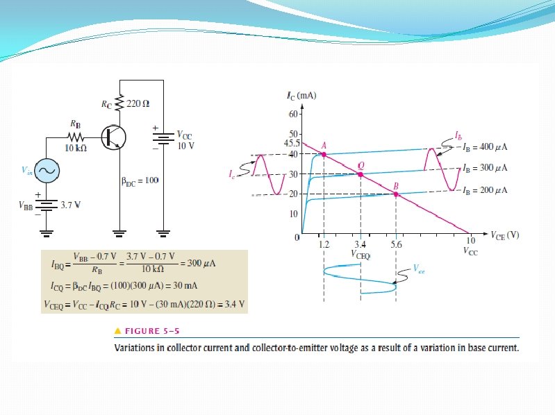
DC Bias establishes the dc operating point (Q-point) for proper linear operation of an amplifier. If an amplifier is not biased with correct dc voltages on the input and output, it can go into saturation or cutoff when an input signal is applied.

FIGURE 5– 3 Illustration of Q-point adjustment.
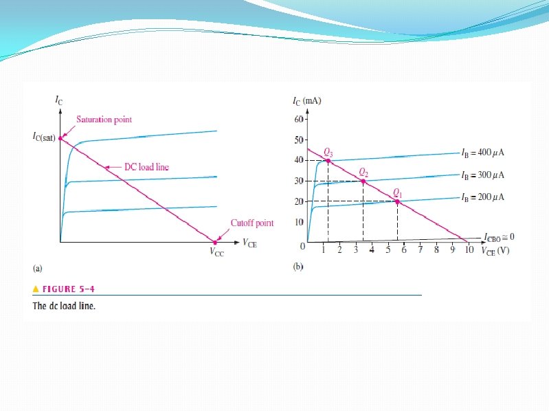

Linear Operation �The region along the load line including all points between saturation and cutoff is generally known as the linear region of the transistor’s operation. As long as the transistor is operated in this region, the output voltage is ideally a linear reproduction of the input.

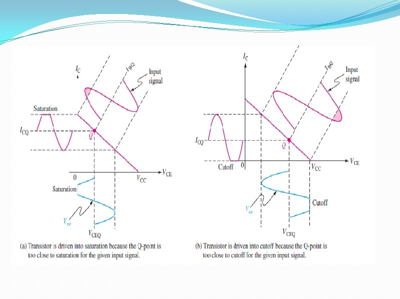
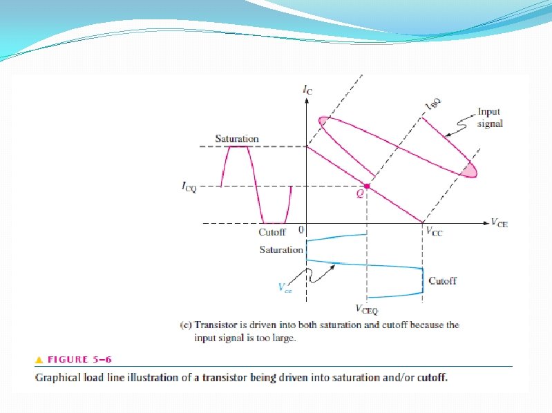
Waveform Distortion under certain input signal conditions the location of the Q-point on the load line can cause one peak of the Vce waveform to be limited or clipped, as shown in parts (a) and (b) of Figure 5– 6. In each case the input signal is too large for the Q-point location and is driving the transistor into cutoff or saturation during a portion of the input cycle. When both peaks are limited as in Figure 5– 6(c), the transistor is being driven into both saturation and cutoff by an excessively large input signal. When only the positive peak is limited, the transistor is being driven into cutoff but not saturation. When only the negative peak is limited, the transistor is being driven into saturation but not cutoff

5– 2 VOLTAGE-DIVIDER BIAS A dc bias voltage at the base of the transistor can be developed by a resistive voltage divider that consists of R 1 and R 2, as shown in Figure 5– 9. VCC is the dc collector supply voltage. Two current paths are between point A and ground: one through R 2 and the other through the base-emitter junction of the transistor and RE. Generally, voltage-divider bias circuits are designed so that the base current is much smaller than the current (I 2) through R 2 in Figure 5– 9. In this case, the voltage-divider circuit is very straightforward to analyze because the loading effect of the base current can be ignored. A voltage divider in which the base current is small compared to the current in R 2 is said to be a stiff voltage divider because the base voltage is relatively independent of different transistors and temperature effects. To analyze a voltagedivider circuit in which IB is small compared to I 2, first calculate the voltage on the base using the unloaded voltage-divider rule:

A voltage divider in which the base current is small compared to the current in R 2 is said to be a stiff voltage divider because the base voltage is relatively independent of different transistors and temperature effects. To analyze a voltage-divider circuit in which IB is small compared to I 2, first calculate the voltage on the base using the unloaded voltage-divider rule:
- Slides: 18