Basic Electronics Chapter 4 Bipolar Junction Transistors 4
 Structure")
Basic Electronics Chapter 4: Bipolar Junction Transistors 4– 1 Bipolar Junction Transistor (BJT) Structure 4– 2 Basic BJT Operation 4– 3 BJT Characteristics and Parameters 4– 4 The BJT as an Amplifier 4– 5 The BJT as a Switch 4– 6 The Phototransistor

◆ Describe the basic structure of the BJT ◆ Discuss basic BJT operation ◆ Discuss basic BJT parameters and characteristics and analyze transistor circuits ◆ Discuss how a BJT is used as a voltage amplifier ◆ Discuss how a BJT is used as a switch ◆ Discuss the phototransistor and its operation

◆ BJT ◆ Emitter ◆ Base ◆ Collector ◆ Gain ◆ Beta ◆ Saturation ◆ Linear ◆ Cutoff ◆ Amplification ◆ Phototransistor
 STRUCTURE �The BJT is constructed with three doped")
4– 1 BIPOLAR JUNCTION TRANSISTOR (BJT) STRUCTURE �The BJT is constructed with three doped semiconductor regions separated by two pn junctions. The three regions are called emitter, base, and collector. �The term bipolar refers to the use of both holes and electrons as current carriers in the transistor structure.
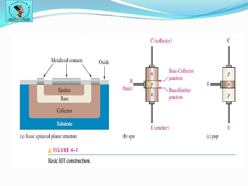

The base region is lightly doped and very thin compared to the heavily doped emitter and the moderately doped collector regions FIGURE 4– 2 Standard BJT (bipolar junction transistor) symbols.

4– 2 BASIC BJT OPERATION In order for a BJT to operate properly as an amplifier, the two pn junctions must be correctly biased with external dc voltages. Figure 4– 3 shows a bias arrangement for both npn and pnp BJTs for operation as an amplifier. Notice that in both cases the base-emitter (BE) junction is forward-biased and the basecollector (BC) junction is reverse-biased. This condition is called forward-reverse bias.

FIGURE 4– 3 Forward-reverse bias of a BJT.

Operation �The heavily doped n-type emitter region has a very high density of conduction-band (free) electrons. These free electrons easily diffuse through the forward based BE junction into the lightly doped and very thin ptype base region. The base has a low density of holes, which are the majority carriers. A small percentage of the total number of free electrons injected into the base region recombine with holes and move as valence electrons through the base region and into the emitter region as hole current.

Transistor dc bias circuits.

The dc current gain of a transistor is the ratio of the dc collector current (IC) to the dc base current (IB) and is designated dc beta ( The ratio of the dc collector current (IC) to the dc emitter current (IE) is the dc alpha ( )). The alpha is a less-used parameter than beta in transistor circuits.


Transistor DC Model The input circuit is a forward-biased diode through which there is base current. The output circuit is a dependent current source with a value that is dependent on the base current, IB. Ideal dc model of an npn transistor.

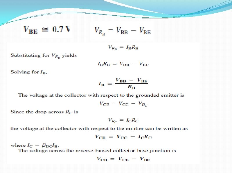
BJT Circuit Analysis Three transistor dc currents and three dc voltages can be identified. Transistor currents and voltages.


Collector Characteristic Curves
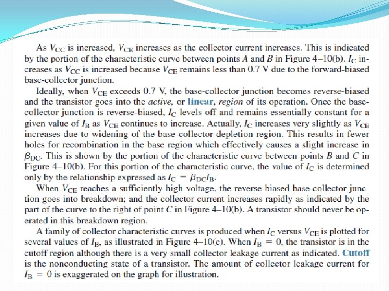

FIGURE 4– 10 Collector characteristic curves.
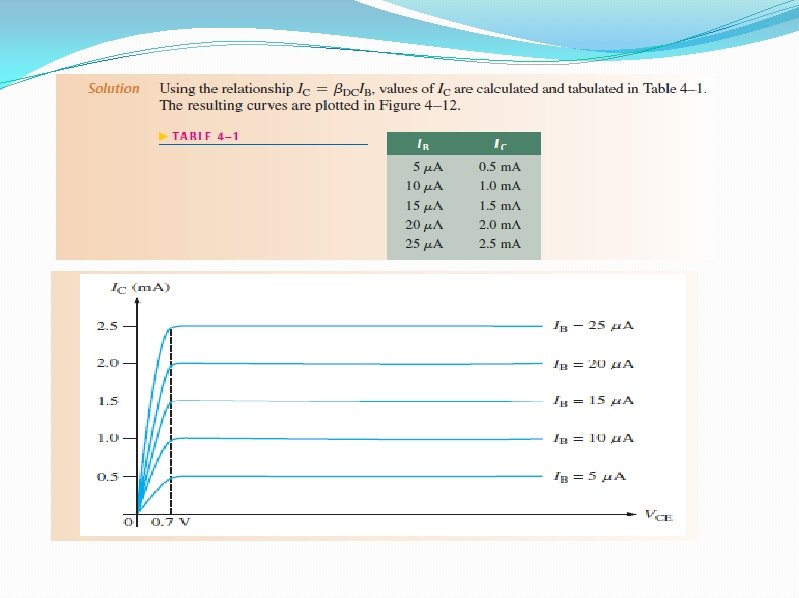

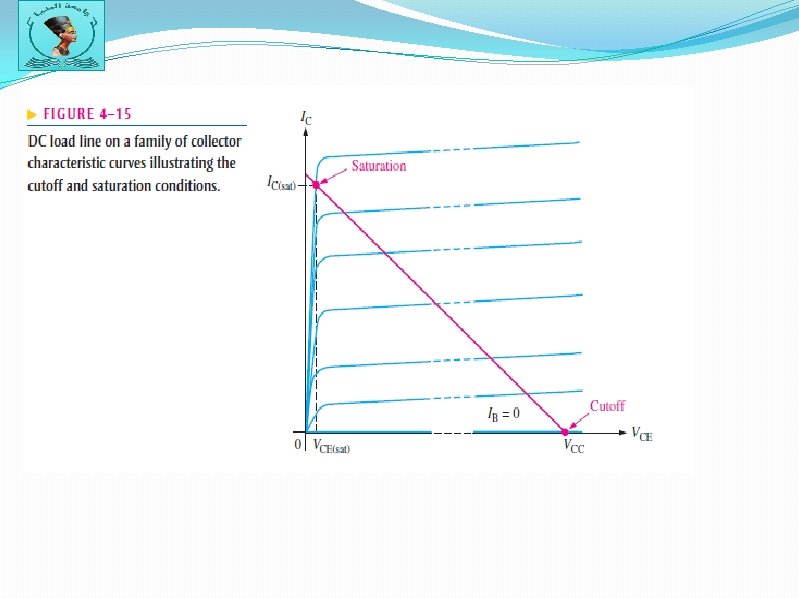
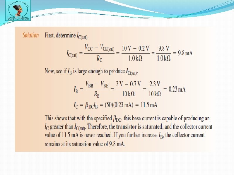
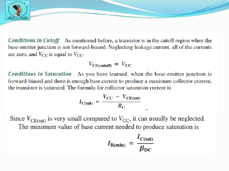
DC Load Line Cutoff and saturation can be illustrated in relation to the collector characteristic curves by the use of a load line. Figure 4– 15 shows a dc load line drawn on a family of curves connecting the cutoff point and the saturation point. The bottom of the load line is at ideal cutoff where IC =0 and VCE =VCC. The top of the load line is at saturation where I C =IC(sat) and VCE =VCE(sat). In between cutoff and saturation along the load line is the active region of the transistor’s operation

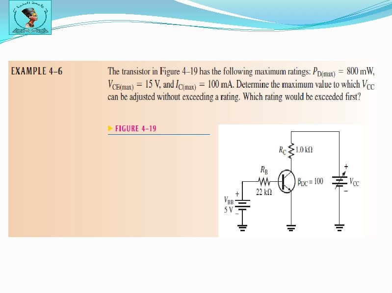
Maximum Transistor Ratings FIGURE 4– 18 Maximum power dissipation curve and tabulated values.

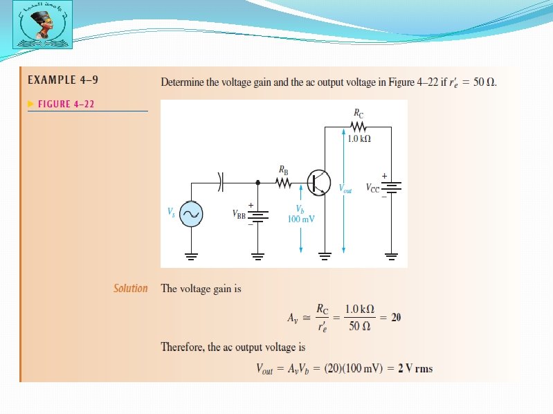
4– 4 THE BJT AS AN AMPLIFIER Amplification is the process of linearly increasing the amplitude of an electrical signal and is one of the major properties of a transistor. When a BJT is biased in the active (or linear) region, the BE junction has a low resistance due to forward bias and the BC junction has a high resistance due to reverse bias. Voltage Amplification a transistor amplifies current because the collector current is equal to the base current multiplied by the current gain. The base current in a transistor is very small compared to the collector.
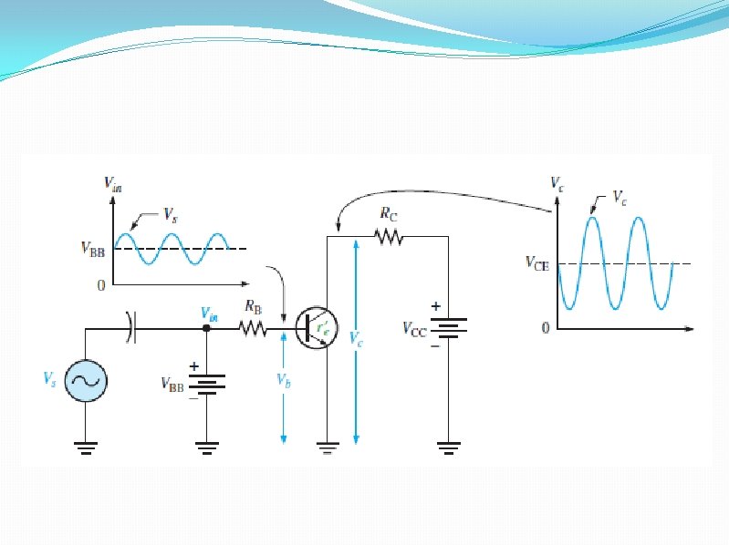

The ac input voltage produces an ac base current The ac collector current produces an ac voltage across RC.

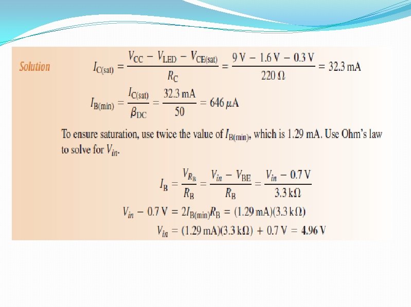
4– 5 THE BJT AS A SWITCH The second major application area is switching applications. When used as an electronic switch, a BJT is normally operated alternately in cutoff and saturation. Many digital circuits use the BJT as a switch. Switching Operation

A Simple Application of a Transistor Switch When the square wave is at 0 V, the transistor is in cutoff; and since there is no collector current, the LED does not emit light. When the square wave goes to its high level, the transistor saturates. This forward-biases the LED, and the resulting collector current through the LED causes it to emit light. Thus, the LED is on for 1 second and off for 1 second.

FIGURE 4– 25

4 -6 The Phototransistor �A phototransistor is similar to a regular BJT except that the base current is produced and controlled by light instead of a voltage source. The phototransistor converts light energy to an electrical signal. �The base current is produced when light strikes the photosensitive semiconductor base region. �When there is no incident light, there is only a small thermally generated collector to emitter leakage current ICEO (called dark current). �When light strikes the collector base junction , a base current Iλ is proportional to the light intensity. �Collector current IC = βDC I λ

�A phototransistor can be either a two-lead or a threelead device. In the three-lead configuration, the base lead is brought out so that the device can be used as a conventional BJT with or without the additional lightsensitivity feature. In the two-lead configuration, the base is not electrically available, and the device can be used only with light as the input. In many applications, the phototransistor is used in the twolead version. Figure 4– 28 shows a phototransistor with a biasing circuit and typical collector characteristic curves. Notice that each individual curve on the graph corresponds to a certain value of light intensity (in this case, the units are m. W/cm 2) and that the collector current increases with light intensity.

FIGURE 4– 28 Phototransistor circuit and typical collector characteristic curves.

Phototransistors are not sensitive to all light but only to light within a certain range of wavelengths. They are most sensitive to particular wavelengths in the red and infrared part of the spectrum,

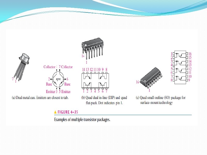
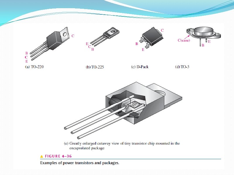
4– 7 TRANSISTOR CATEGORIES AND PACKAGING Transistor Categories �General-Purpose/Small-Signal Transistors Generalpurpose/small-signal transistors are generally used for low- or medium-power amplifiers or switching circuits. �Power Transistors Power transistors are used to handle large currents (typically more than 1 A) and/or large voltages. For example, the final audio stage in a stereo system uses a power transistor amplifier to drive the speakers.

Transistor package

- Slides: 53