
Basic Electronics Chapter 2 Diodes and Applications 2
Basic Electronics Chapter 2: Diodes and Applications 2– 1 Diode Operation 2– 2 Voltage-Current (V-I) Characteristics of a Diode 2– 3 Diode Models 2– 4 Half-Wave Rectifiers 2– 5 Full-Wave Rectifiers 2– 6 Power Supply Filters and Regulators 2– 7 Diode Limiters and Clampers 2– 8 Voltage Multipliers
◆ Use a diode in common applications ◆ Analyze the voltage-current (V-I) characteristic of a diode ◆ Explain how the three diode models differ ◆ Explain and analyze the operation of half-wave rectifiers ◆ Explain and analyze the operation of full-wave rectifiers ◆ Explain and analyze power supply filters and regulators ◆ Explain and analyze the operation of diode limiters and clampers ◆ Explain and analyze the operation of diode voltage multipliers

◆ Diode ◆ Bias ◆ Forward bias ◆ Reverse bias ◆ V-I characteristic ◆ DC power supply ◆ Rectifier ◆ Filter ◆ Regulator ◆ Half-wave rectifier ◆ Peak inverse voltage (PIV) ◆ Full-wave rectifier ◆ Ripple voltage ◆ Line regulation ◆ Load regulation ◆ Limiter ◆ Clamper

2– 1 DIODE OPERATION �diode is made from a small piece of semiconductor material, usually silicon, in which half is doped as a p region and half is doped as an n region with a pn junction and depletion region in between. The p region is called the anode and is connected to a conductive terminal. The n region is called the cathode and is connected to a seconductive terminal
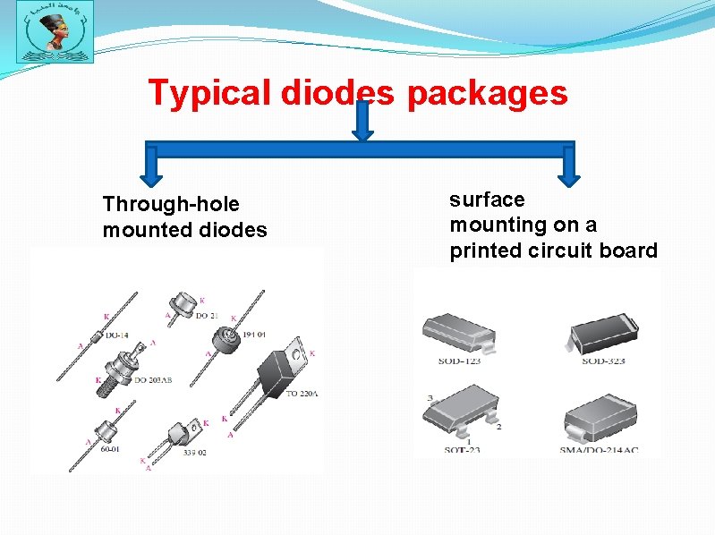
Typical diodes packages Through-hole mounted diodes surface mounting on a printed circuit board
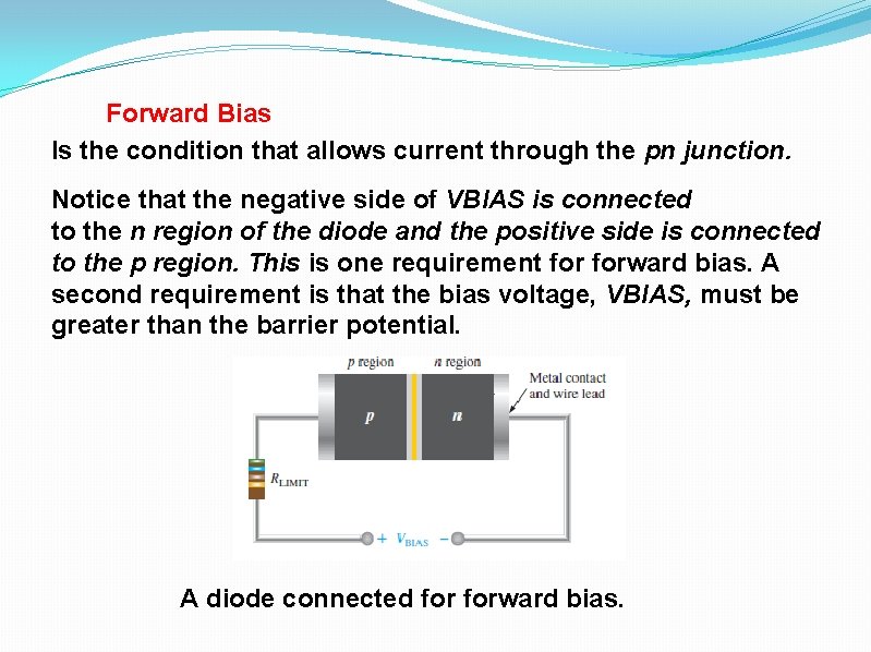
Forward Bias Is the condition that allows current through the pn junction. Notice that the negative side of VBIAS is connected to the n region of the diode and the positive side is connected to the p region. This is one requirement forward bias. A second requirement is that the bias voltage, VBIAS, must be greater than the barrier potential. A diode connected forward bias.
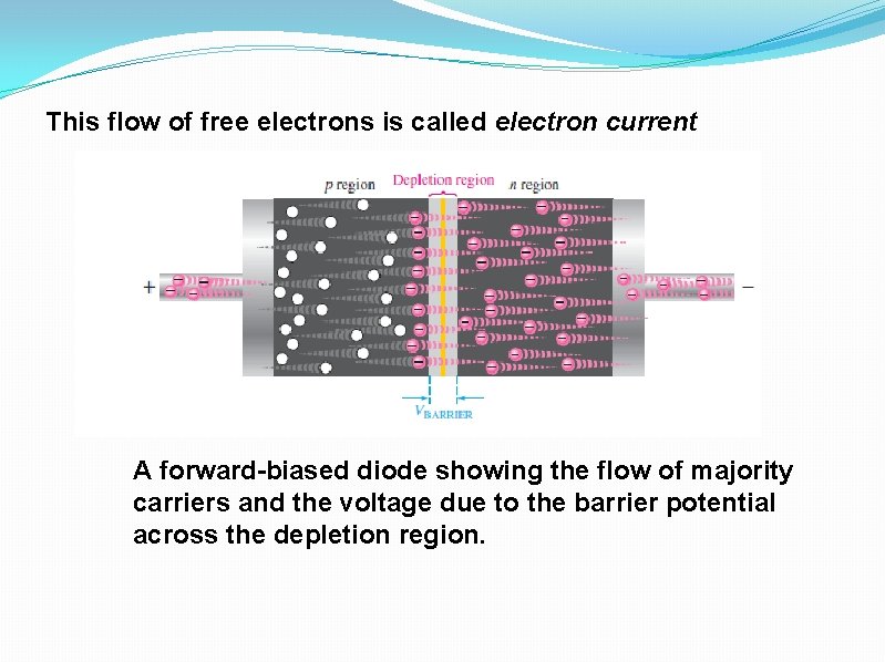
This flow of free electrons is called electron current A forward-biased diode showing the flow of majority carriers and the voltage due to the barrier potential across the depletion region.
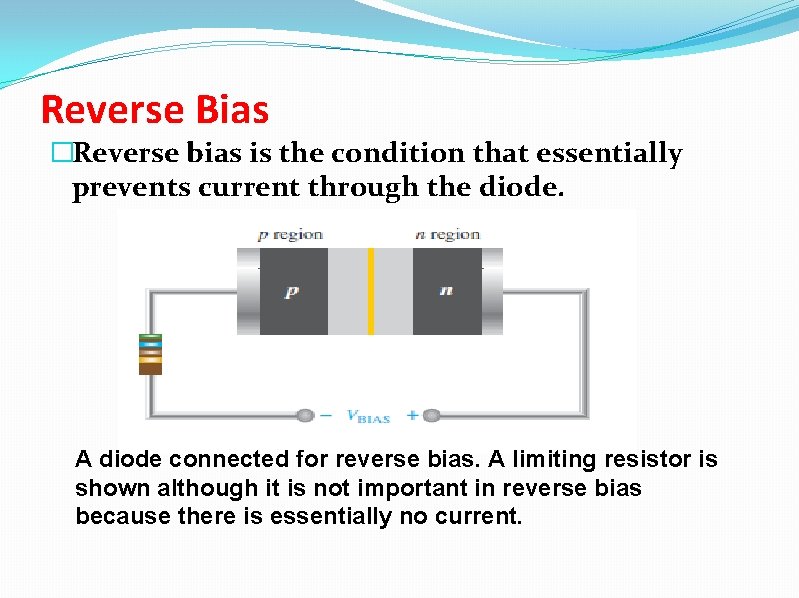
Reverse Bias �Reverse bias is the condition that essentially prevents current through the diode. A diode connected for reverse bias. A limiting resistor is shown although it is not important in reverse bias because there is essentially no current.
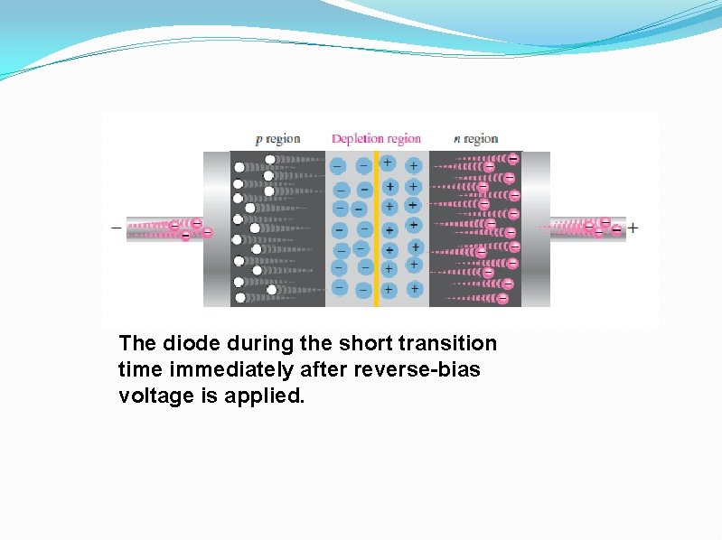
The diode during the short transition time immediately after reverse-bias voltage is applied.
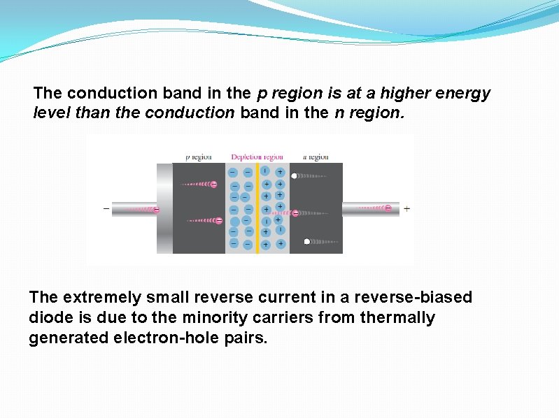
The conduction band in the p region is at a higher energy level than the conduction band in the n region. The extremely small reverse current in a reverse-biased diode is due to the minority carriers from thermally generated electron-hole pairs.
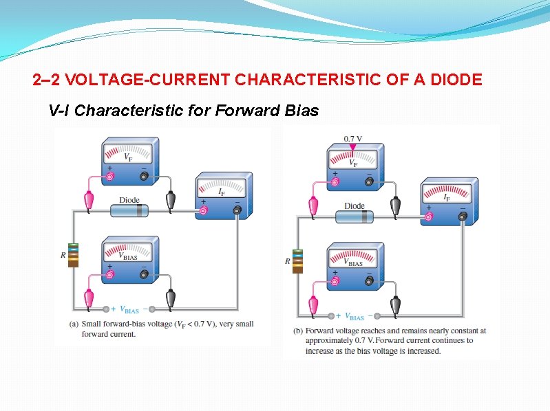
2– 2 VOLTAGE-CURRENT CHARACTERISTIC OF A DIODE V-I Characteristic for Forward Bias
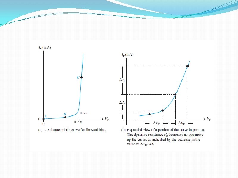
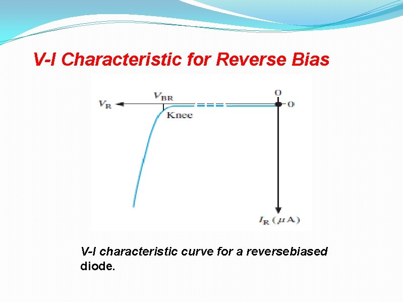
V-I Characteristic for Reverse Bias V-I characteristic curve for a reversebiased diode.
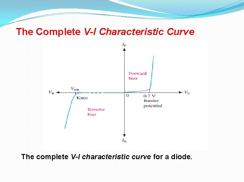
The Complete V-I Characteristic Curve The complete V-I characteristic curve for a diode.
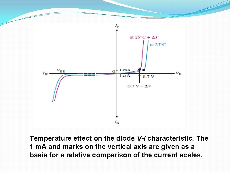
Temperature effect on the diode V-I characteristic. The 1 m. A and marks on the vertical axis are given as a basis for a relative comparison of the current scales.
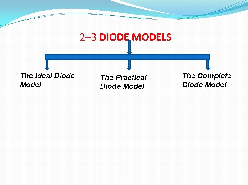
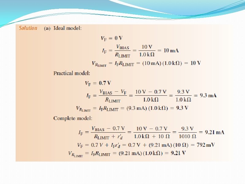
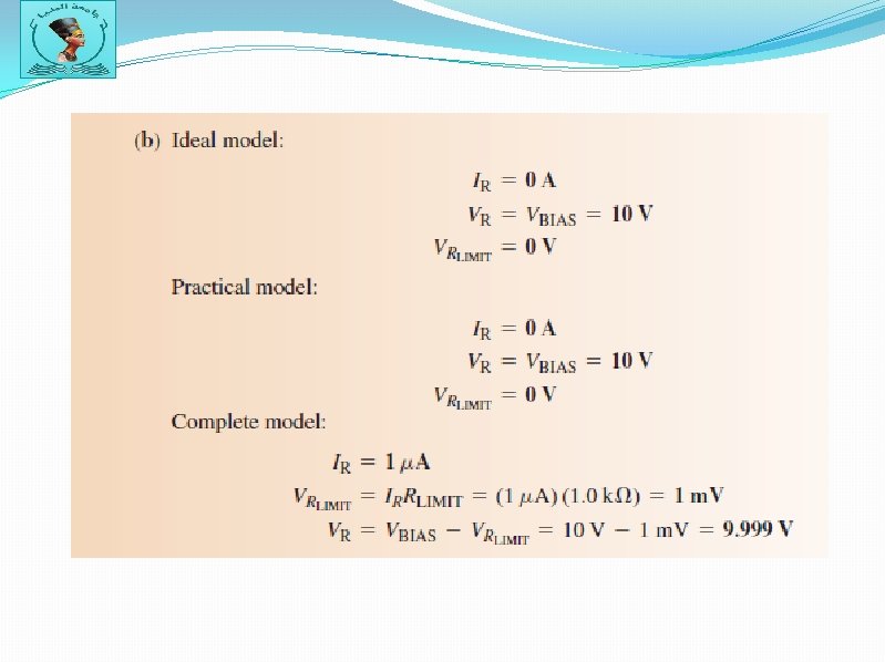
2– 3 DIODE MODELS The Ideal Diode Model The Practical Diode Model The Complete Diode Model
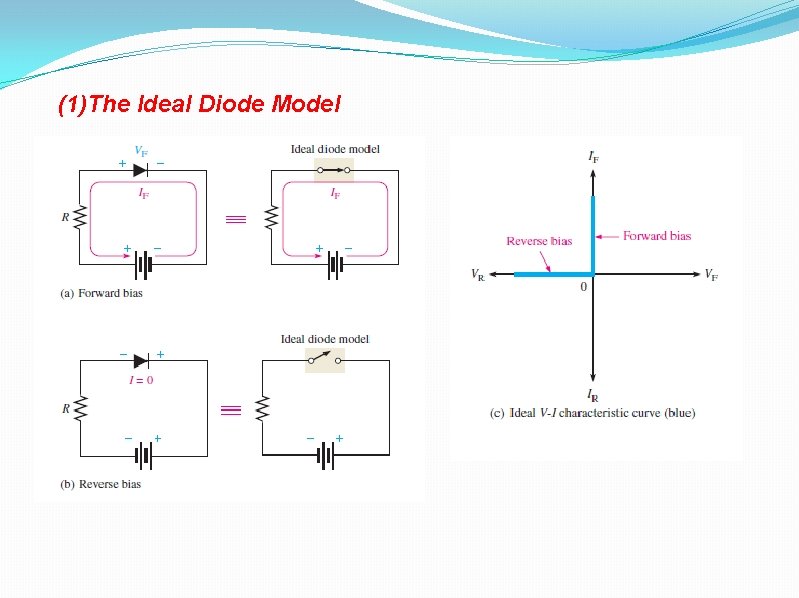
(1)The Ideal Diode Model
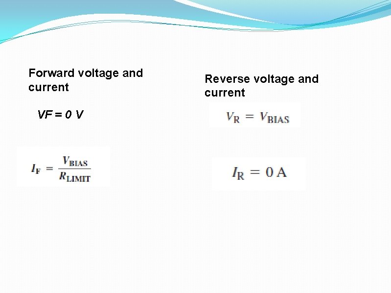
Forward voltage and current VF = 0 V Reverse voltage and current
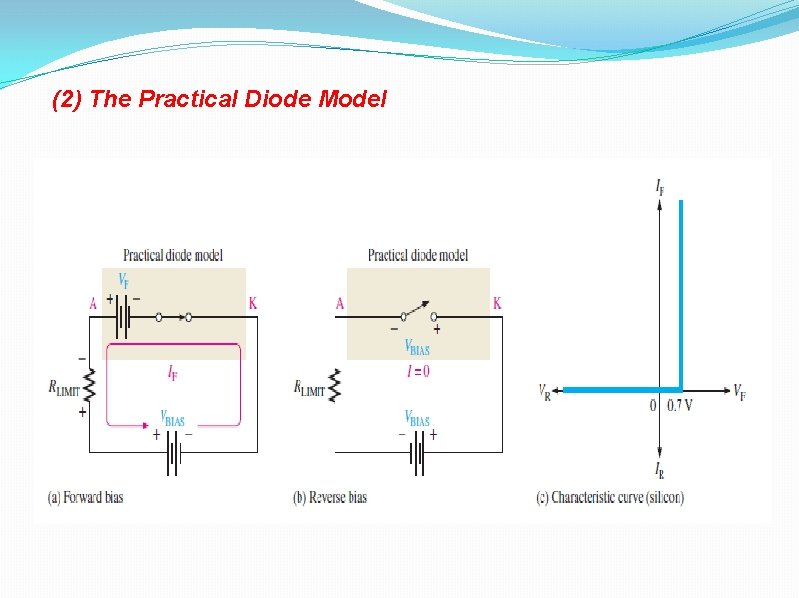
(2) The Practical Diode Model
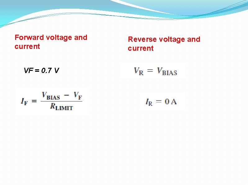
Forward voltage and current VF = 0. 7 V Reverse voltage and current
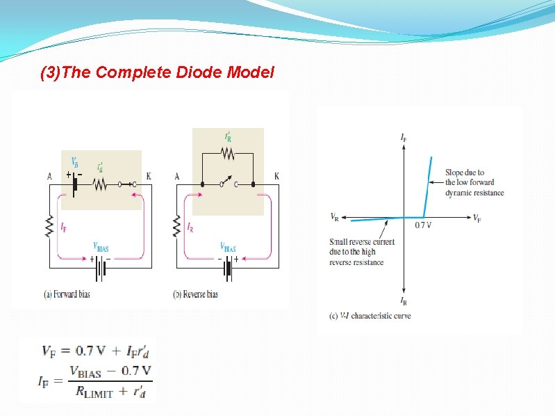
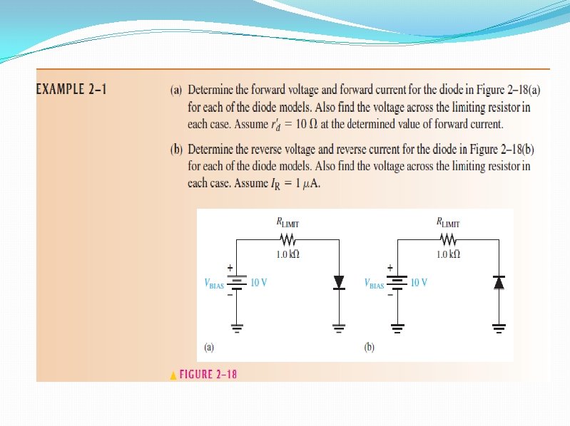
(3)The Complete Diode Model
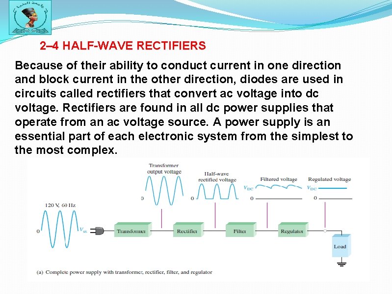
2– 4 HALF-WAVE RECTIFIERS Because of their ability to conduct current in one direction and block current in the other direction, diodes are used in circuits called rectifiers that convert ac voltage into dc voltage. Rectifiers are found in all dc power supplies that operate from an ac voltage source. A power supply is an essential part of each electronic system from the simplest to the most complex.
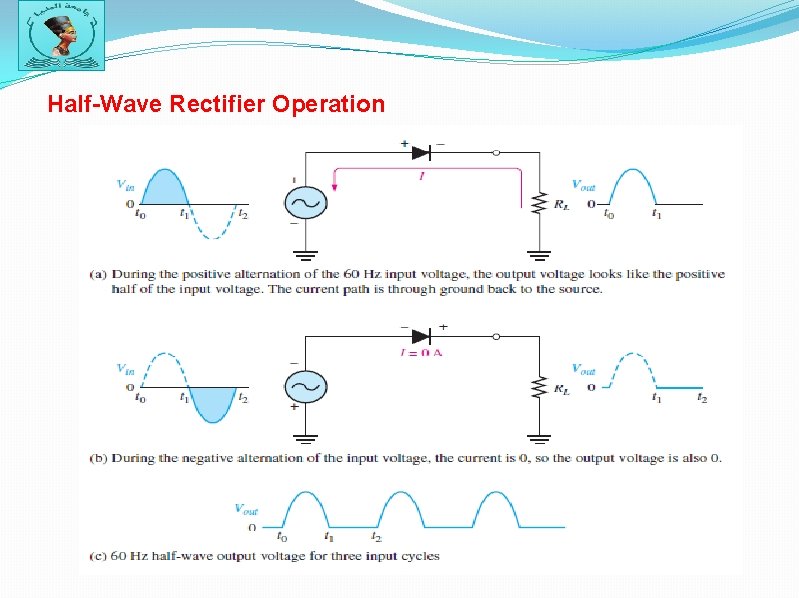
Half-Wave Rectifier Operation
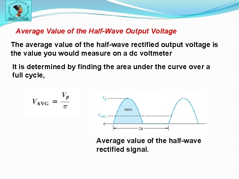
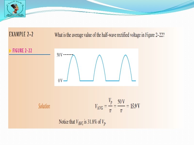
Average Value of the Half-Wave Output Voltage The average value of the half-wave rectified output voltage is the value you would measure on a dc voltmeter It is determined by finding the area under the curve over a full cycle, Average value of the half-wave rectified signal.
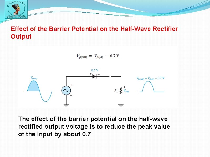
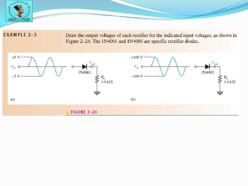
Effect of the Barrier Potential on the Half-Wave Rectifier Output The effect of the barrier potential on the half-wave rectified output voltage is to reduce the peak value of the input by about 0. 7
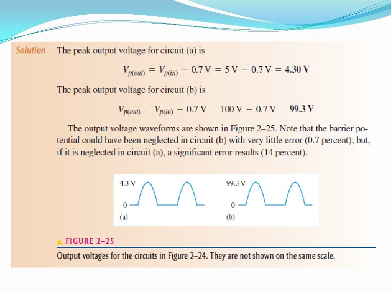

Peak Inverse Voltage (PIV) The peak inverse voltage (PIV) equals the peak value of the input voltage. For the diode in Figure 2– 26, the maximum value of reverse voltage, designated as PIV, occurs at the peak of each negative alternation of the input voltage when the diode is reverse-biased The PIV occurs at the peak of each half-cycle of the input voltage when the diode is reverse-biased. In this circuit, the PIV occurs at the peak of each negative half-cycle.
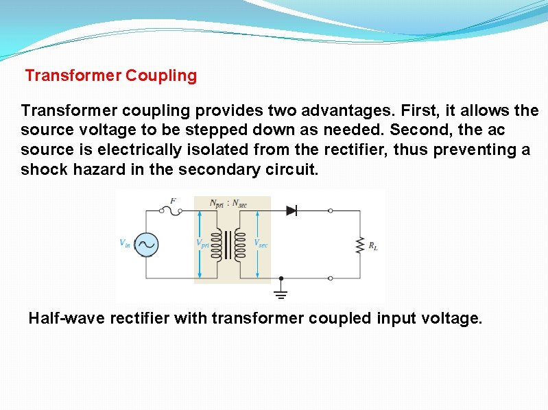
Transformer Coupling Transformer coupling provides two advantages. First, it allows the source voltage to be stepped down as needed. Second, the ac source is electrically isolated from the rectifier, thus preventing a shock hazard in the secondary circuit. Half-wave rectifier with transformer coupled input voltage.
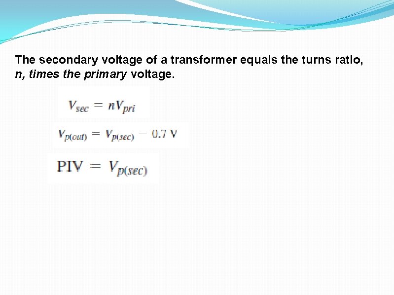
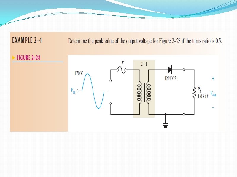
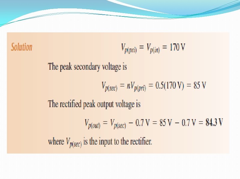
The secondary voltage of a transformer equals the turns ratio, n, times the primary voltage.
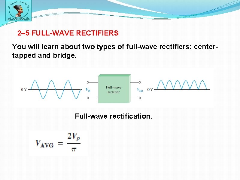
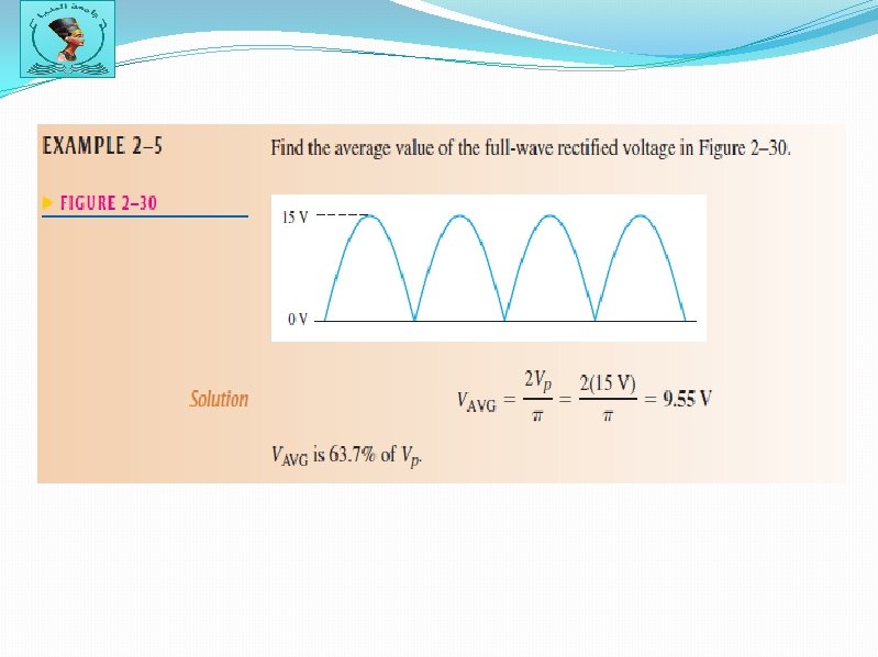
2– 5 FULL-WAVE RECTIFIERS You will learn about two types of full-wave rectifiers: centertapped and bridge. Full-wave rectification.
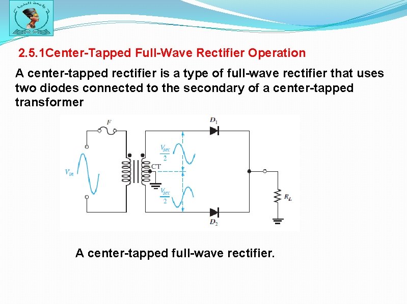
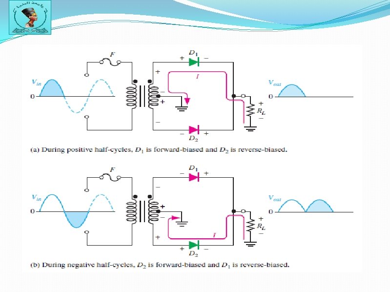
2. 5. 1 Center-Tapped Full-Wave Rectifier Operation A center-tapped rectifier is a type of full-wave rectifier that uses two diodes connected to the secondary of a center-tapped transformer A center-tapped full-wave rectifier.
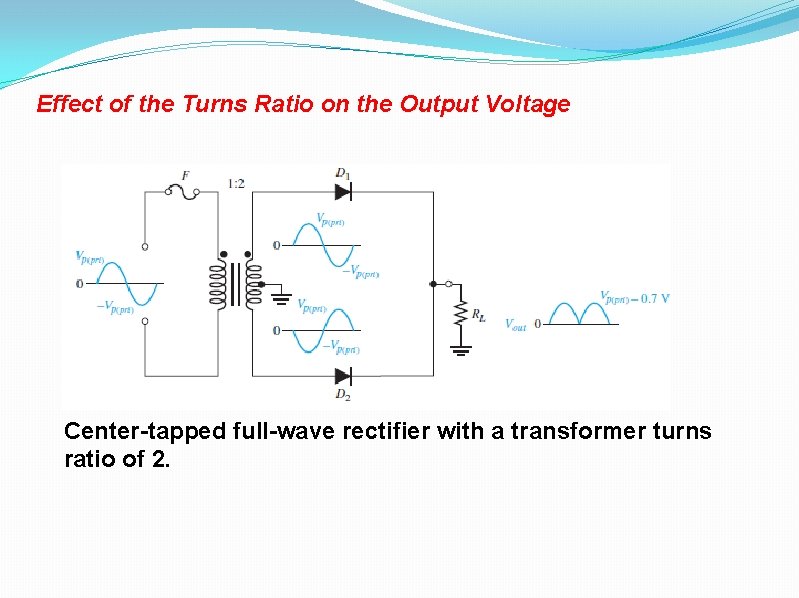
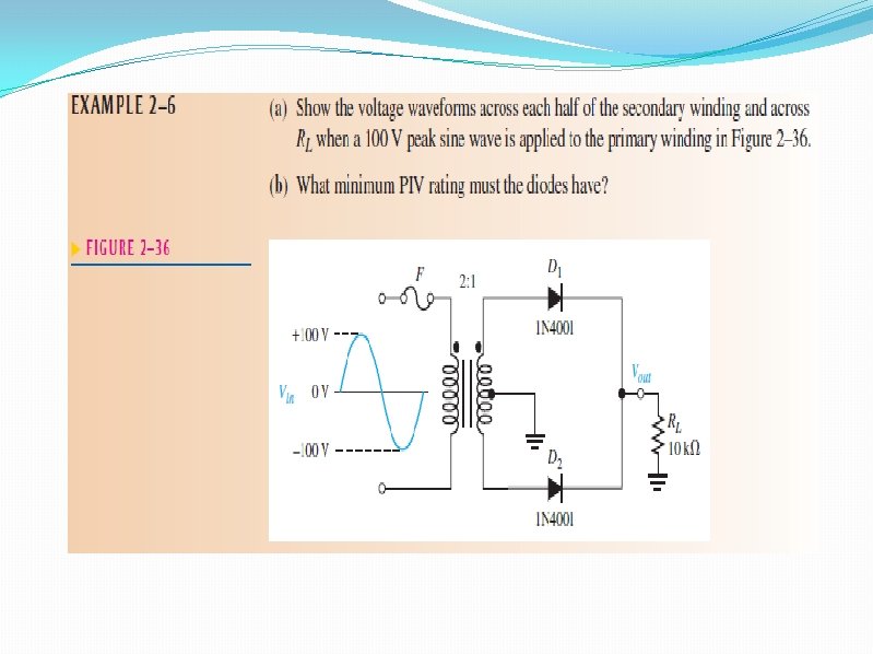
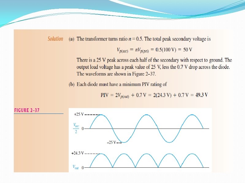
Effect of the Turns Ratio on the Output Voltage Center-tapped full-wave rectifier with a transformer turns ratio of 2.
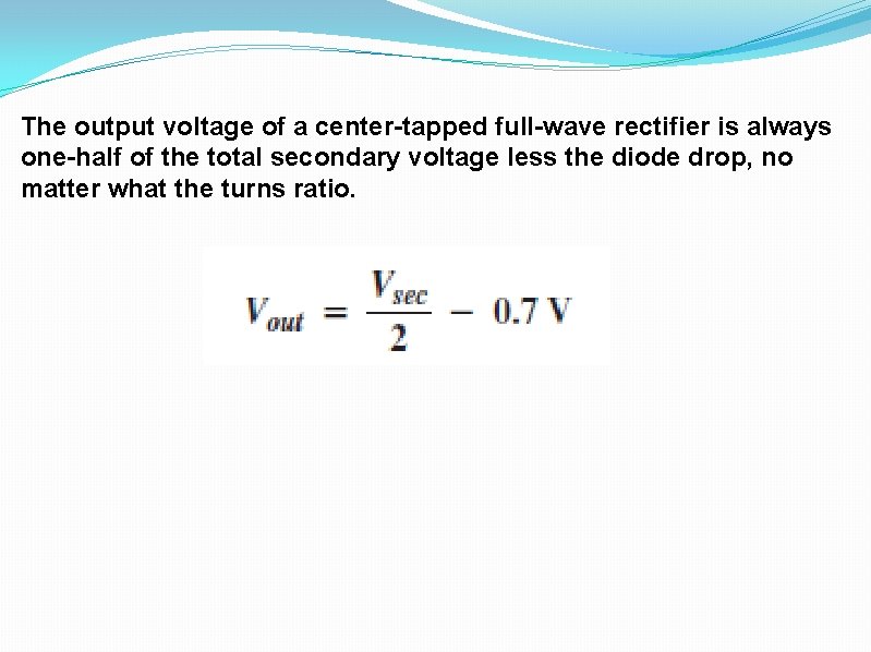
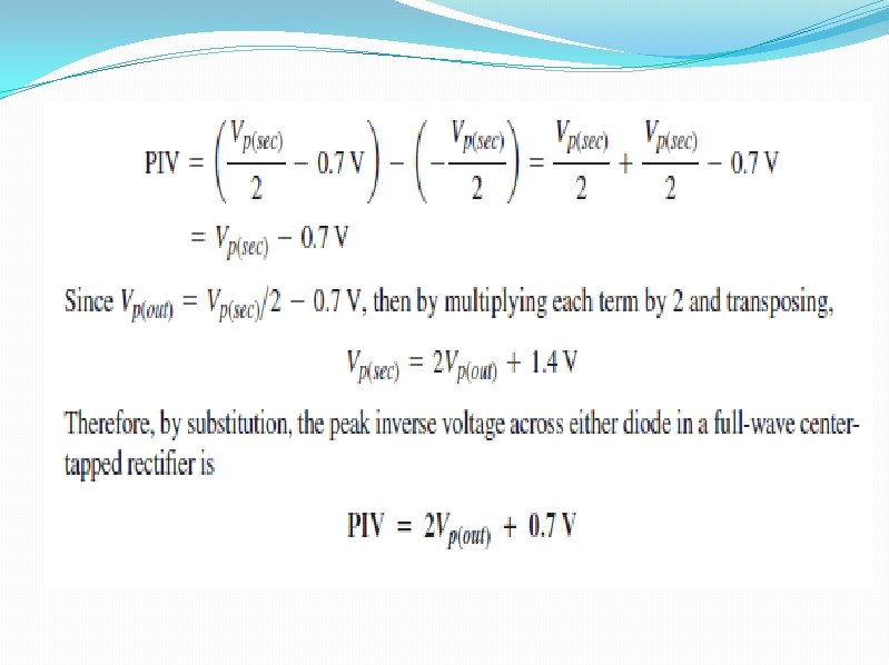
The output voltage of a center-tapped full-wave rectifier is always one-half of the total secondary voltage less the diode drop, no matter what the turns ratio.
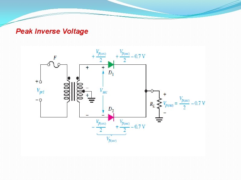
Peak Inverse Voltage
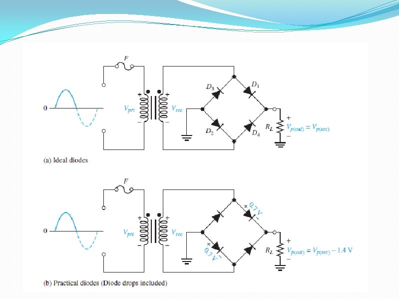
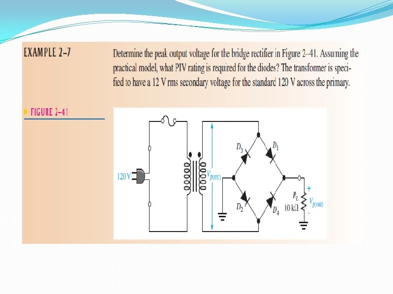
2. 5. 2 Bridge Full-Wave Rectifier Operation
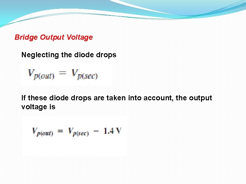
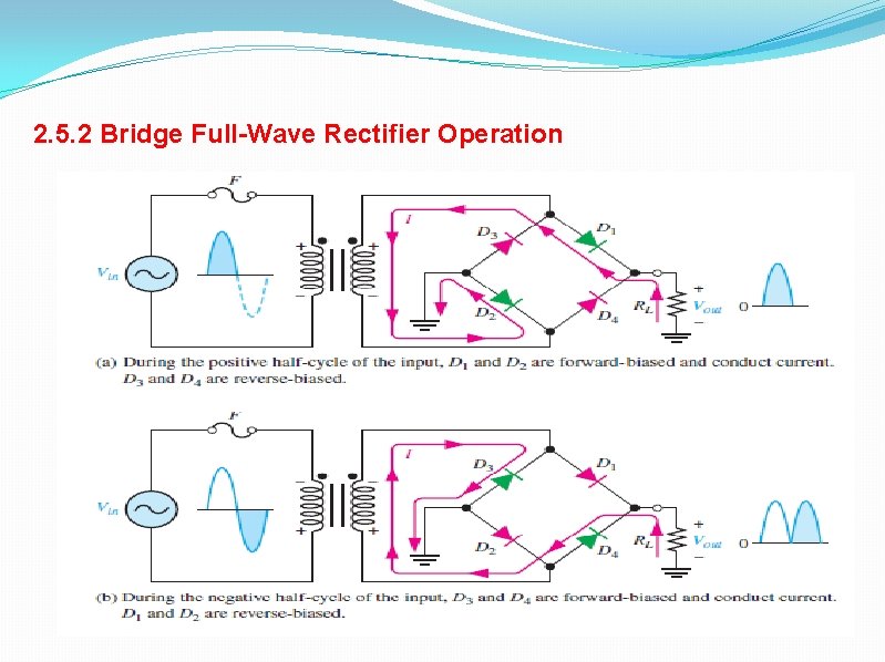
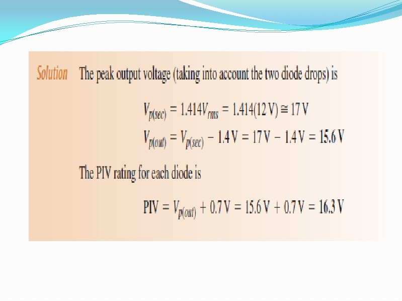
Bridge Output Voltage Neglecting the diode drops If these diode drops are taken into account, the output voltage is
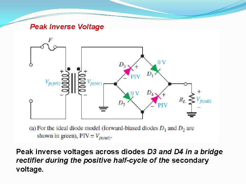
Peak Inverse Voltage Peak inverse voltages across diodes D 3 and D 4 in a bridge rectifier during the positive half-cycle of the secondary voltage.
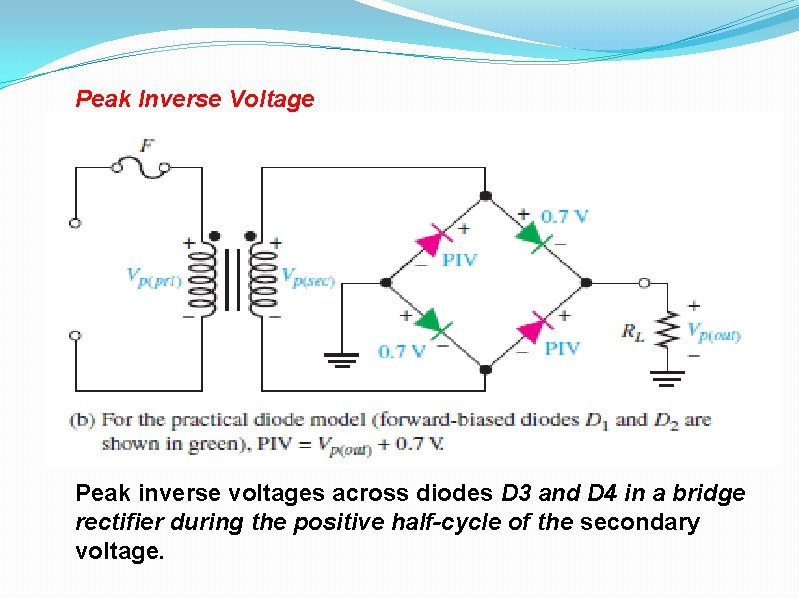
Peak Inverse Voltage Peak inverse voltages across diodes D 3 and D 4 in a bridge rectifier during the positive half-cycle of the secondary voltage.
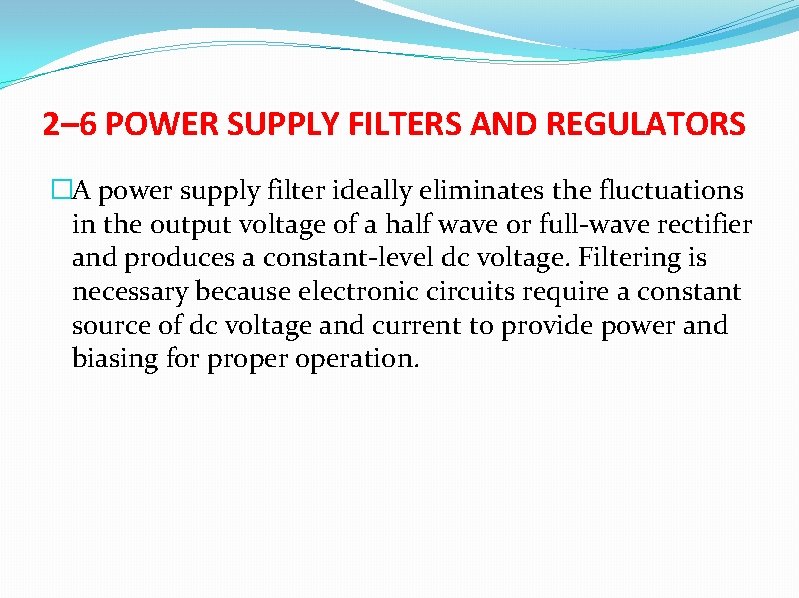
2– 6 POWER SUPPLY FILTERS AND REGULATORS �A power supply filter ideally eliminates the fluctuations in the output voltage of a half wave or full-wave rectifier and produces a constant-level dc voltage. Filtering is necessary because electronic circuits require a constant source of dc voltage and current to provide power and biasing for properation.
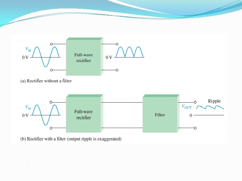
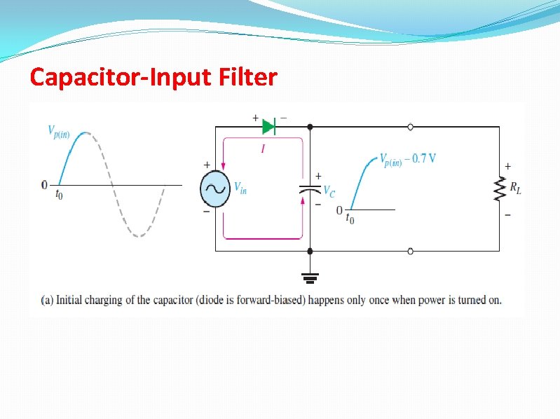
Capacitor-Input Filter
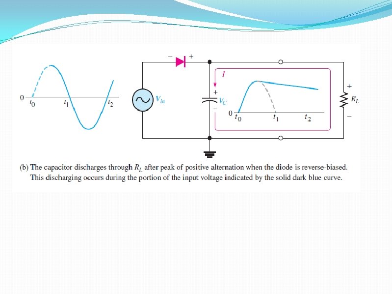
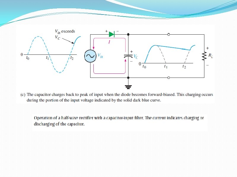
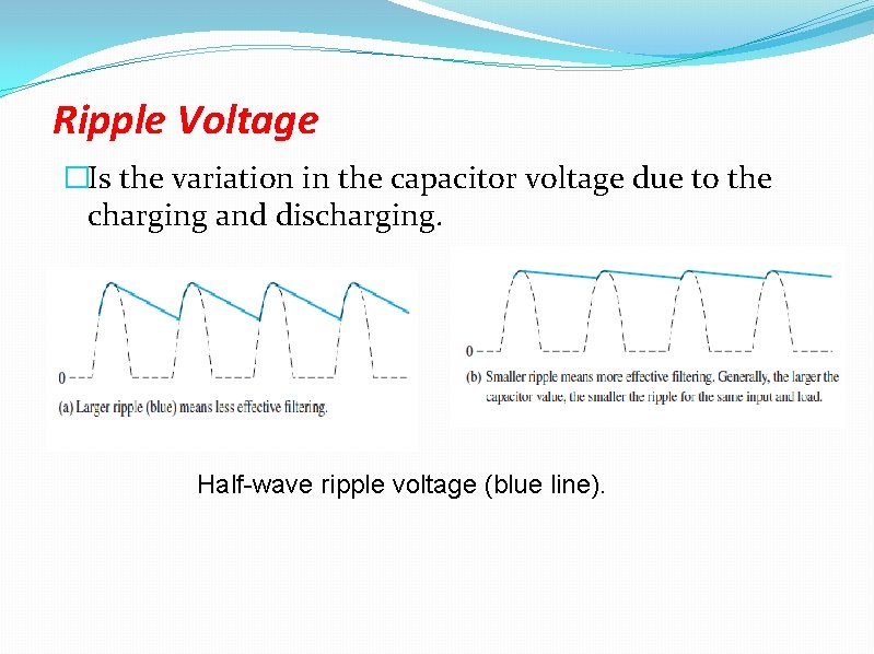
Ripple Voltage �Is the variation in the capacitor voltage due to the charging and discharging. Half-wave ripple voltage (blue line).
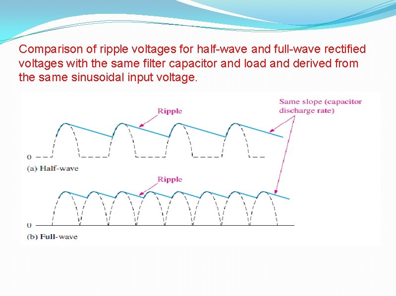
Comparison of ripple voltages for half-wave and full-wave rectified voltages with the same filter capacitor and load and derived from the same sinusoidal input voltage.
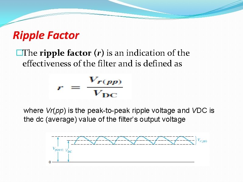
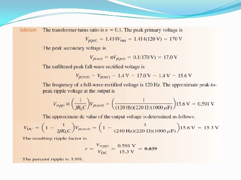
Ripple Factor �The ripple factor (r) is an indication of the effectiveness of the filter and is defined as where Vr(pp) is the peak-to-peak ripple voltage and VDC is the dc (average) value of the filter’s output voltage
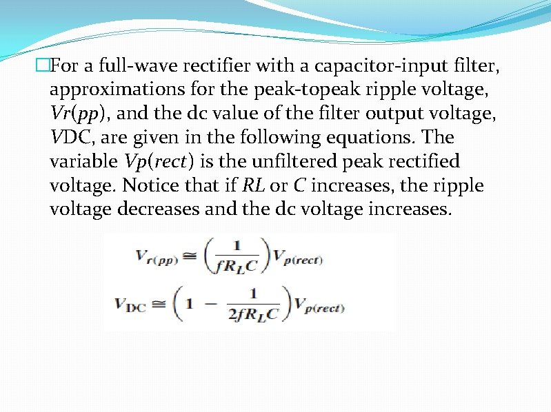
�For a full-wave rectifier with a capacitor-input filter, approximations for the peak-topeak ripple voltage, Vr(pp), and the dc value of the filter output voltage, VDC, are given in the following equations. The variable Vp(rect) is the unfiltered peak rectified voltage. Notice that if RL or C increases, the ripple voltage decreases and the dc voltage increases.
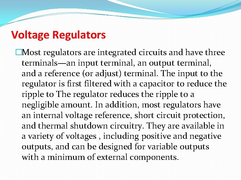
Voltage Regulators �Most regulators are integrated circuits and have three terminals—an input terminal, an output terminal, and a reference (or adjust) terminal. The input to the regulator is first filtered with a capacitor to reduce the ripple to The regulator reduces the ripple to a negligible amount. In addition, most regulators have an internal voltage reference, short circuit protection, and thermal shutdown circuitry. They are available in a variety of voltages , including positive and negative outputs, and can be designed for variable outputs with a minimum of external components.
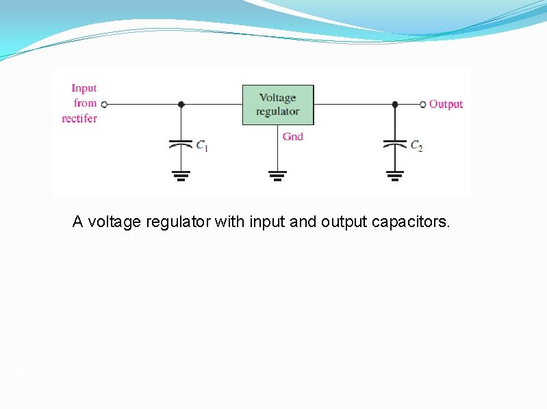
A voltage regulator with input and output capacitors.
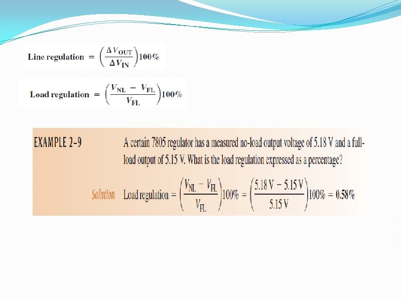
Percent Regulation �The regulation expressed as a percentage is a figure of merit used to specify the performance of a voltage regulator. It can be in terms of input (line) regulation or load regulation. �The line regulation specifies how much change occurs in the output voltage for a given change in the input voltage. �The load regulation specifies how much change occurs in the output voltage over a certain range of load current values, usually from minimum current (no load, NL) to maximum current (full load, FL).
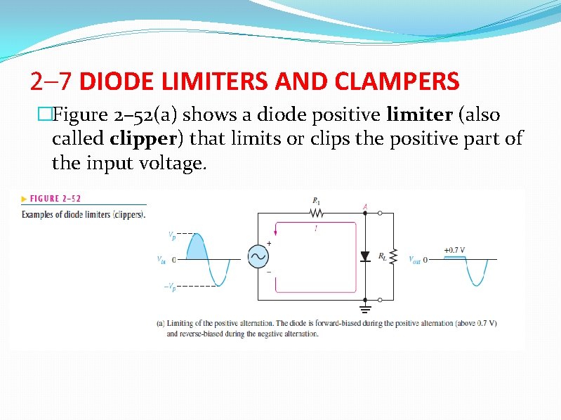
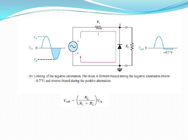
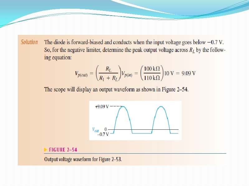
2– 7 DIODE LIMITERS AND CLAMPERS �Figure 2– 52(a) shows a diode positive limiter (also called clipper) that limits or clips the positive part of the input voltage.
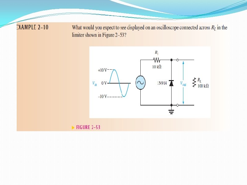
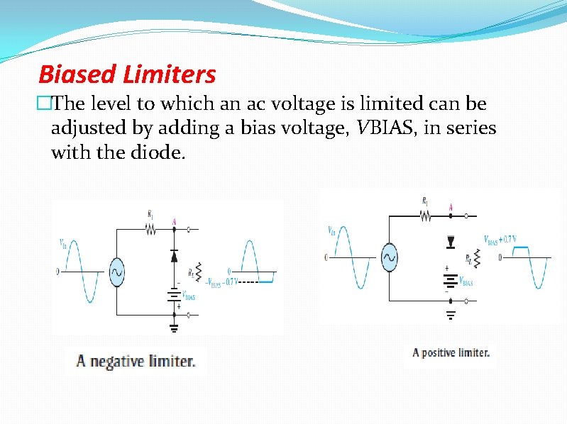
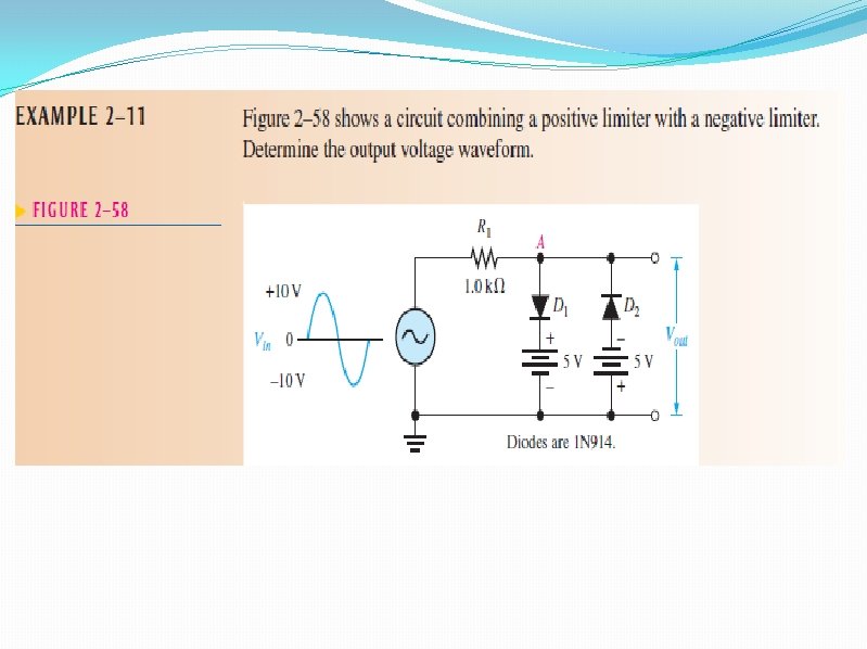
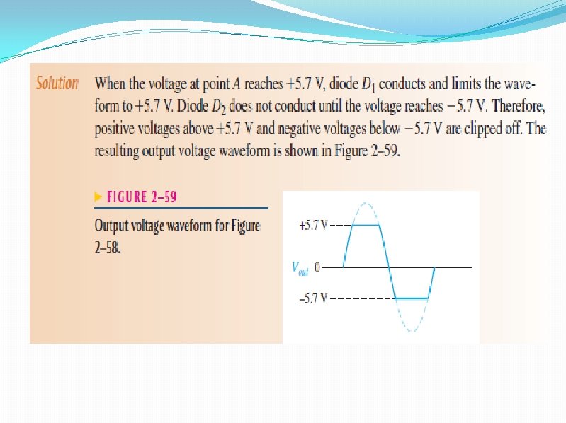
Biased Limiters �The level to which an ac voltage is limited can be adjusted by adding a bias voltage, VBIAS, in series with the diode.
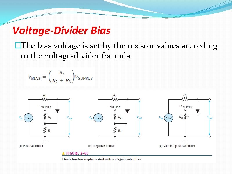
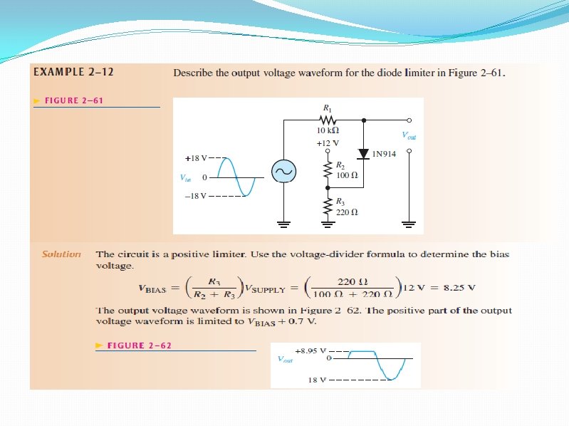
Voltage-Divider Bias �The bias voltage is set by the resistor values according to the voltage-divider formula.
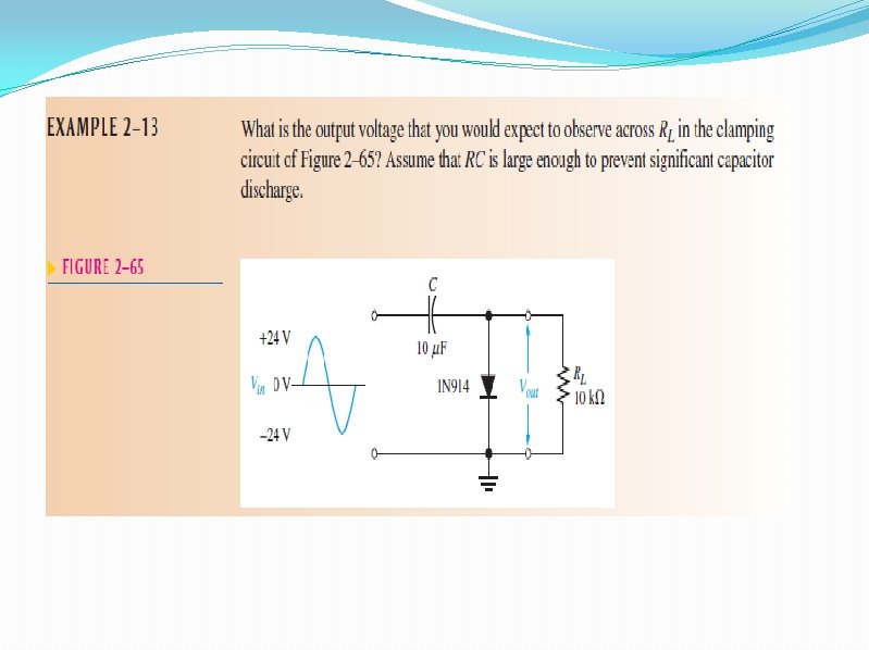
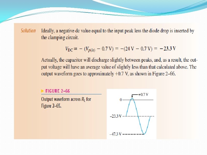
Diode Clampers �A clamper adds a dc level to an ac voltage. Clampers are sometimes known as dc restorers.
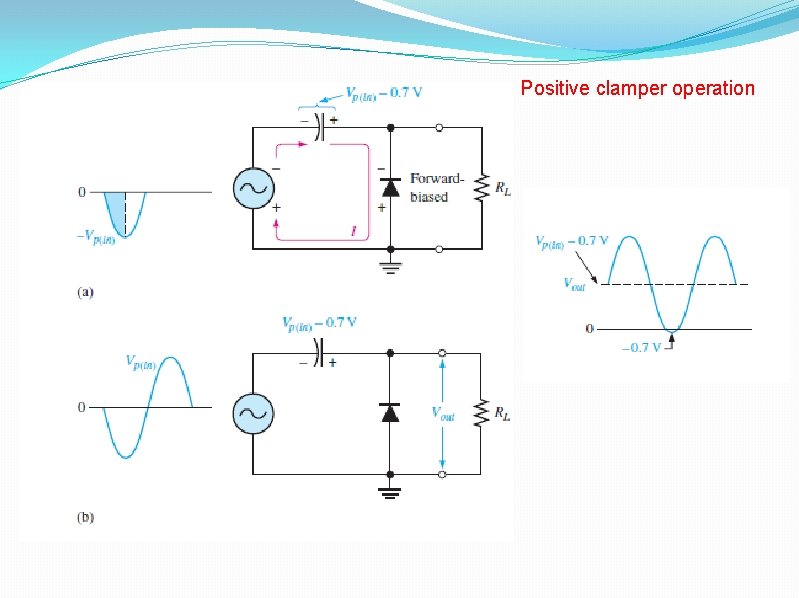
Positive clamper operation
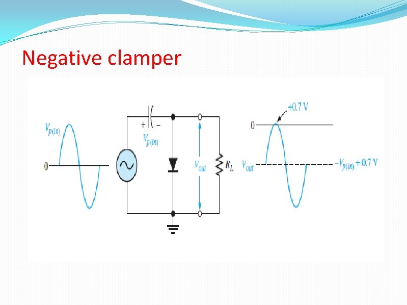
Negative clamper
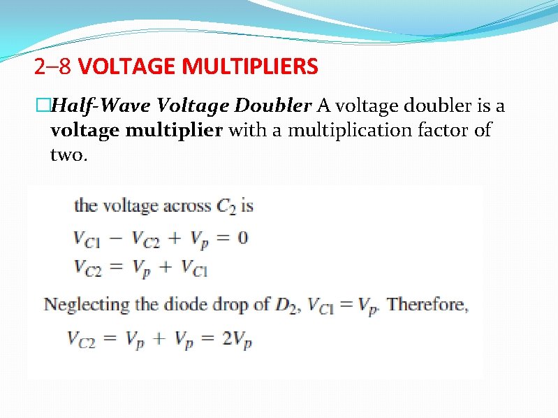
2– 8 VOLTAGE MULTIPLIERS �Half-Wave Voltage Doubler A voltage doubler is a voltage multiplier with a multiplication factor of two.
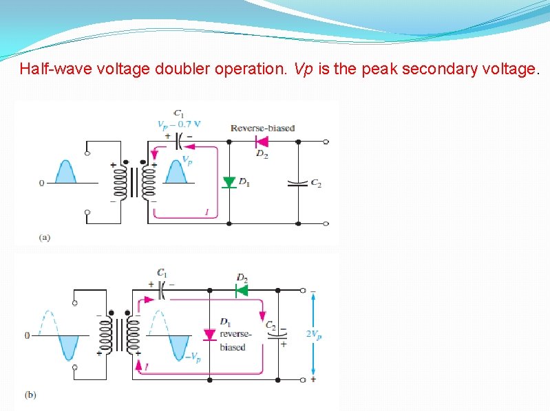
Half-wave voltage doubler operation. Vp is the peak secondary voltage.
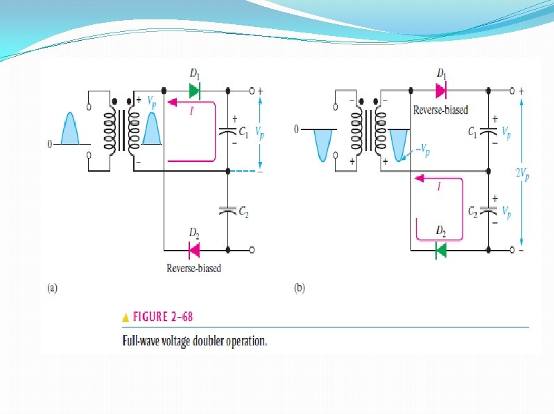
Full-Wave Voltage Doubler �A full-wave doubler is shown in Figure 2– 68. When the secondary voltage is positive, D 1 is forward-biased and C 1 charges to approximately Vp, as shown in part (a). During the negative half-cycle, D 2 is forwardbiased and C 2 charges to approximately Vp, as shown in part (b). The output voltage, 2 Vp, is taken across the two capacitors in series.

- Slides: 87