BASIC DIGITAL LOGIC CIRCUITS DESIGN By Tarun joshi
BASIC DIGITAL LOGIC CIRCUITS DESIGN By Tarun joshi Deepak Bhataniya Lavkesh Patidar OER Submission IIT Bombay. X FDP 201 x on Pedagogy for Online and Blended Teaching-Learning Process, is licensed under the Creative Commons Attribution-Share. Alike 4. 0 International License. You are free to use, distribute and modify it, including for commercial purposes, provided you acknowledge the source and share-alike. To view a copy of this license, visit http: //creativecommons. org/licenses/by-sa/4. 0/ 12/25/2021 DIGITAL LOGIC DESIGN
Introduction • This open education resource prepared and submitted as a part of AICTE approved FDP conducted by IIT Bombay, course PPT on “BASIC DIGITAL LOGIC & CIRCUIT DESIGN” with Examples , Boolean Expressions , Circuit Design Examples that can be used to learn and clarify certain basics of DIGITAL LOGIC & CIRCUIT DESIGN. The Example Problems in ppt can provide basic cognitive learning levels of revised Bloom’s taxonomy like Recall, Understand Apply levels. • There are 6 different topics of DIGITAL LOGIC & CIRCUIT DESIGN: Binary logic and Gates , Boolean Algebra, Standard and Canonical Forms, Karnaugh Maps (K-Maps), K-Map Manipulation, More Logic Gates (Universal Gates). • This Will be useful for Digital Electronics Topics Taught in First year B. E. /B Tech (UG)students (any domain), & Second Year B. E. /B Tech (UG)students of Electrical, Electronics & Computer Science. • This resource is licensed under CC-BY-SA ver 4. 0. You are free to use, distribute and modify it, including for commercial purposes, provided you acknowledge the source and share-alike. To see more details about the license, visit http: //creativecommons. org/licenses/by-sa/4. 0/ 12/25/2021 DIGITAL LOGIC DESIGN
Overview • Binary logic and Gates • Boolean Algebra – Basic Properties – Algebraic Manipulation • Standard and Canonical Forms – Minterms and Maxterms (Canonical forms) – SOP and POS (Standard forms) • Karnaugh Maps (K-Maps) – 2, 3, 4, and 5 variable maps – Simplification using K-Maps • K-Map Manipulation – Implicants: Prime, Essential – Don’t Cares • More Logic Gates (Universal Gates) 12/25/2021 DIGITAL LOGIC DESIGN
Binary Logic • Deals with binary variables that take 2 discrete values (0 and 1), and with logic operations • Three basic logic operations: – AND, OR, NOT • Binary/logic variables are typically represented as letters: A, B, C, …, X, Y, Z 12/25/2021 DIGITAL LOGIC DESIGN

Binary Logic Function F(vars) = expression n. Operators set of binary variables n. Variables n. Constants ( 0, 1 ) n. Groupings (parenthesis) Example: F(a, b) = a’ • b + b’ G(x, y, z) = x • (y+z’) 12/25/2021 ( +, • , ‘ ) DIGITAL LOGIC DESIGN
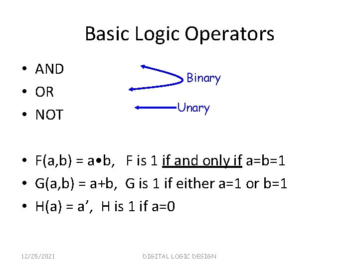
Basic Logic Operators • AND • OR • NOT Binary Unary • F(a, b) = a • b, F is 1 if and only if a=b=1 • G(a, b) = a+b, G is 1 if either a=1 or b=1 • H(a) = a’, H is 1 if a=0 12/25/2021 DIGITAL LOGIC DESIGN
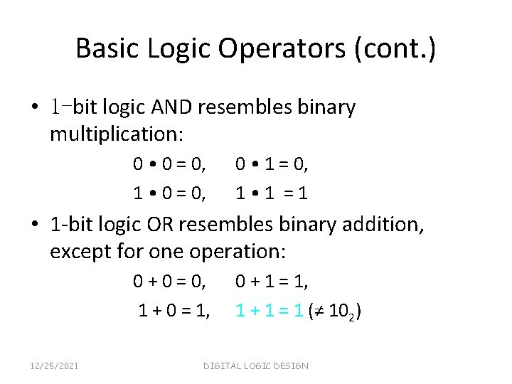
Basic Logic Operators (cont. ) • 1 -bit logic AND resembles binary multiplication: 0 • 0 = 0, 1 • 0 = 0, 0 • 1 = 0, 1 • 1 =1 • 1 -bit logic OR resembles binary addition, except for one operation: 0 + 0 = 0, 1 + 0 = 1, 12/25/2021 0 + 1 = 1, 1 + 1 = 1 (≠ 102) DIGITAL LOGIC DESIGN
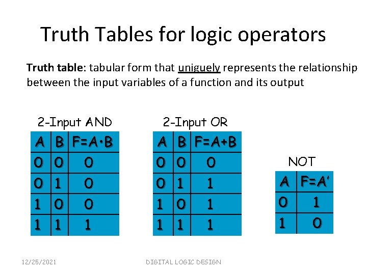
Truth Tables for logic operators Truth table: tabular form that uniguely represents the relationship between the input variables of a function and its output 2 -Input AND A 0 0 1 1 B F=A • B 0 0 1 0 0 0 1 1 12/25/2021 2 -Input OR A 0 0 1 1 B F=A+B 0 0 1 1 1 DIGITAL LOGIC DESIGN NOT A F=A’ 0 1 1 0
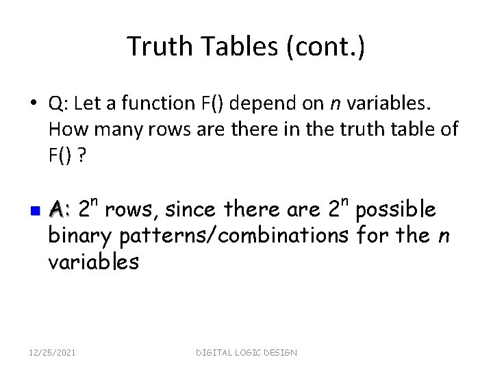
Truth Tables (cont. ) • Q: Let a function F() depend on n variables. How many rows are there in the truth table of F() ? n n n A: 2 rows, since there are 2 possible binary patterns/combinations for the n variables 12/25/2021 DIGITAL LOGIC DESIGN
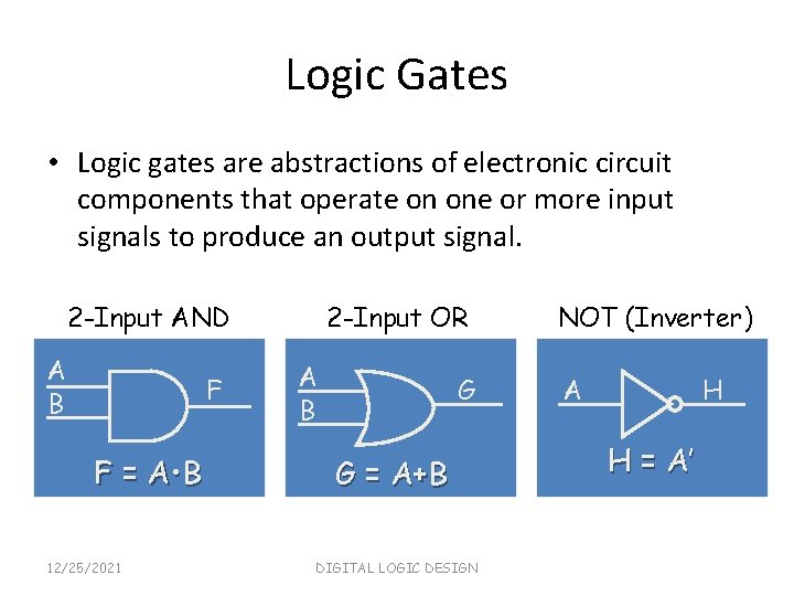
Logic Gates • Logic gates are abstractions of electronic circuit components that operate on one or more input signals to produce an output signal. 2 -Input AND A B F F = A • B 12/25/2021 2 -Input OR A B G G = A+B DIGITAL LOGIC DESIGN NOT (Inverter) A H H = A’
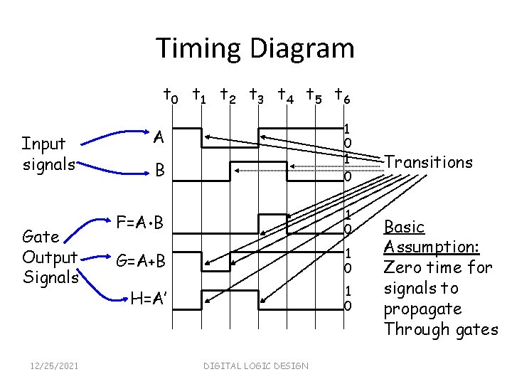
Timing Diagram t 0 t 1 t 2 t 3 t 4 t 5 t 6 Input signals Gate Output Signals 12/25/2021 B 1 0 F=A • B 1 0 G=A+B 1 0 H=A’ 1 0 A DIGITAL LOGIC DESIGN Transitions Basic Assumption: Zero time for signals to propagate Through gates
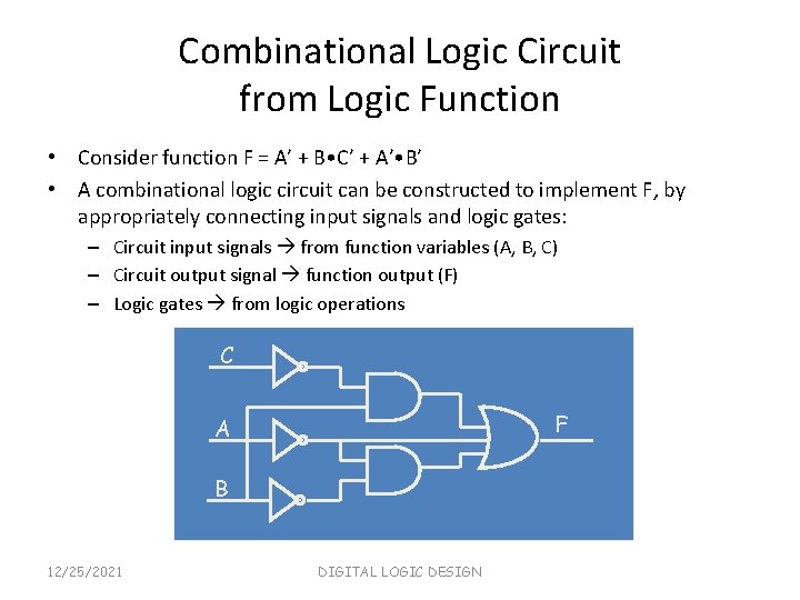
Combinational Logic Circuit from Logic Function • Consider function F = A’ + B • C’ + A’ • B’ • A combinational logic circuit can be constructed to implement F, by appropriately connecting input signals and logic gates: – Circuit input signals from function variables (A, B, C) – Circuit output signal function output (F) – Logic gates from logic operations C F A B 12/25/2021 DIGITAL LOGIC DESIGN
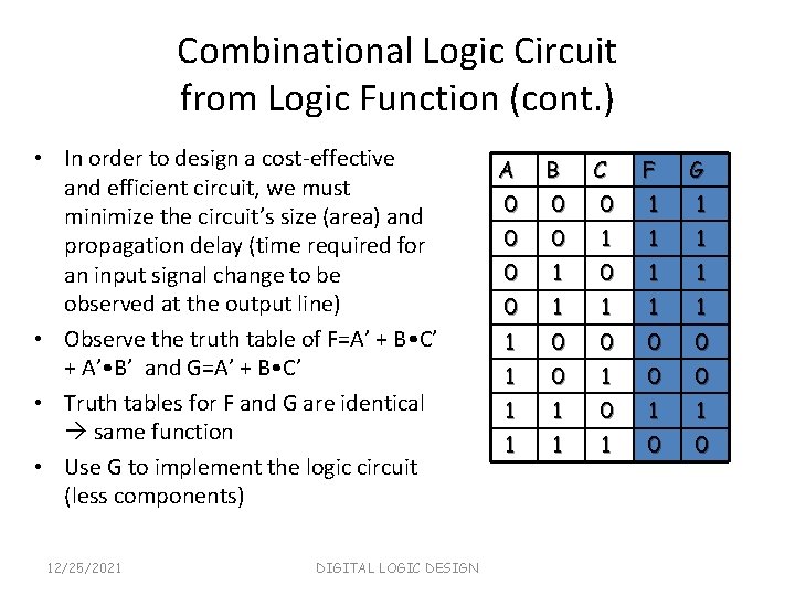
Combinational Logic Circuit from Logic Function (cont. ) • In order to design a cost-effective and efficient circuit, we must minimize the circuit’s size (area) and propagation delay (time required for an input signal change to be observed at the output line) • Observe the truth table of F=A’ + B • C’ + A’ • B’ and G=A’ + B • C’ • Truth tables for F and G are identical same function • Use G to implement the logic circuit (less components) 12/25/2021 DIGITAL LOGIC DESIGN A B C F G 0 0 0 1 1 1 0 1 1 1 0 0 1 1 1 1 1 0 0
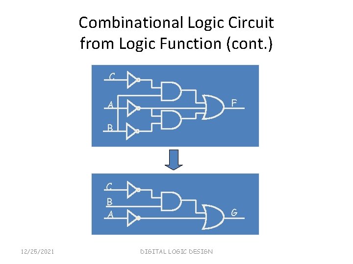
Combinational Logic Circuit from Logic Function (cont. ) C F A B C B A 12/25/2021 G DIGITAL LOGIC DESIGN
Boolean Algebra • VERY nice machinery used to manipulate (simplify) Boolean functions • George Boole (1815 -1864): “An investigation of the laws of thought” • Terminology: – Literal: A variable or its complement – Product term: literals connected by • – Sum term: literals connected by + 12/25/2021 DIGITAL LOGIC DESIGN
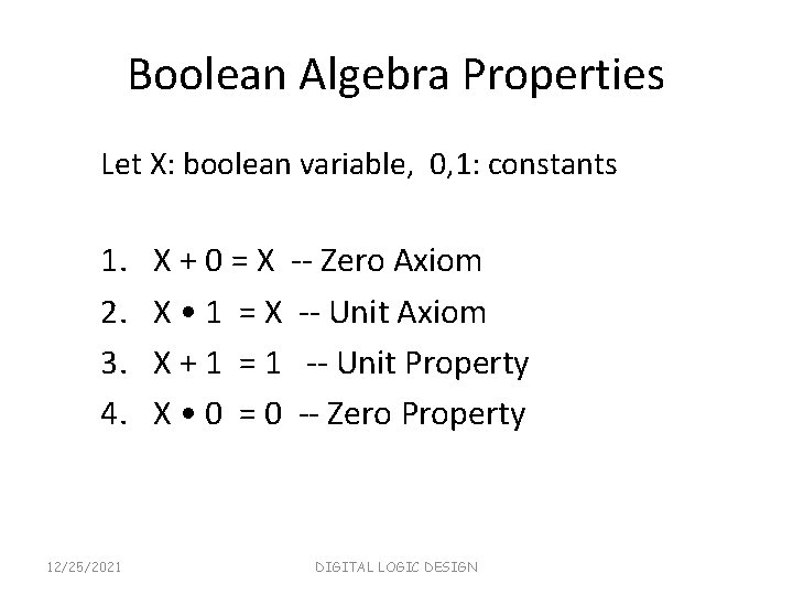
Boolean Algebra Properties Let X: boolean variable, 0, 1: constants 1. 2. 3. 4. 12/25/2021 X + 0 = X -- Zero Axiom X • 1 = X -- Unit Axiom X + 1 = 1 -- Unit Property X • 0 = 0 -- Zero Property DIGITAL LOGIC DESIGN
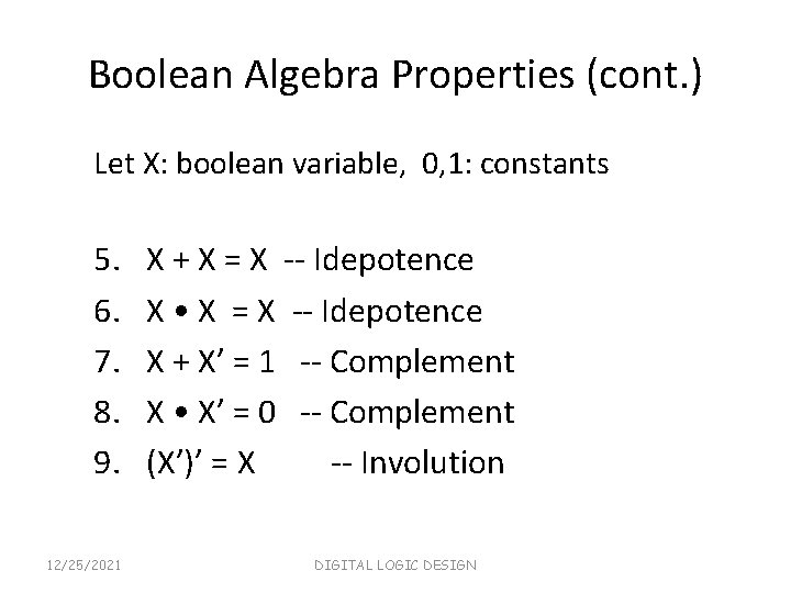
Boolean Algebra Properties (cont. ) Let X: boolean variable, 0, 1: constants 5. 6. 7. 8. 9. 12/25/2021 X + X = X -- Idepotence X • X = X -- Idepotence X + X’ = 1 -- Complement X • X’ = 0 -- Complement (X’)’ = X -- Involution DIGITAL LOGIC DESIGN
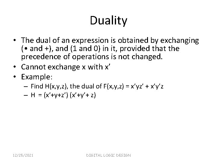
Duality • The dual of an expression is obtained by exchanging ( • and +), and (1 and 0) in it, provided that the precedence of operations is not changed. • Cannot exchange x with x’ • Example: – Find H(x, y, z), the dual of F(x, y, z) = x’yz’ + x’y’z – H = (x’+y+z’) (x’+y’+ z) 12/25/2021 DIGITAL LOGIC DESIGN
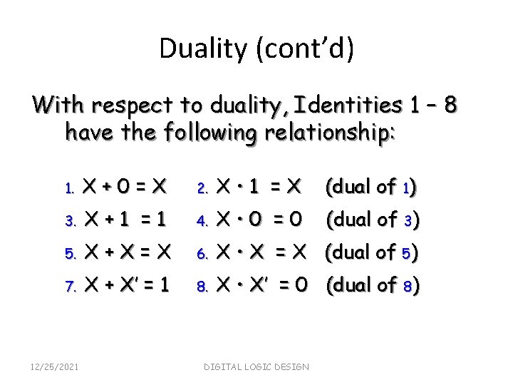
Duality (cont’d) With respect to duality, Identities 1 – 8 have the following relationship: 1. X+0=X 2. X • 1 =X (dual of 1) 3. X+1 =1 4. X • 0 =0 (dual of 3) 5. X+X=X 6. X • X = X (dual of 5) 7. X + X’ = 1 8. X • X’ = 0 (dual of 8) 12/25/2021 DIGITAL LOGIC DESIGN
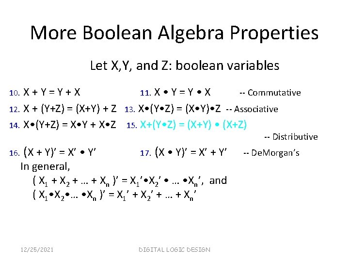
More Boolean Algebra Properties Let X, Y, and Z: boolean variables X+Y=Y+X 12. X + (Y+Z) = (X+Y) + Z 14. X • (Y+Z) = X • Y + X • Z 10. 16. (X + Y)’ = X’ • Y’ X • Y=Y • X -- Commutative 13. X • (Y • Z) = (X • Y) • Z -- Associative 15. X+(Y • Z) = (X+Y) • (X+Z) 11. -- Distributive 17. (X • Y)’ = X’ + Y’ In general, ( X 1 + X 2 + … + Xn )’ = X 1’ • X 2’ • … • Xn’, and ( X 1 • X 2 • … • Xn )’ = X 1’ + X 2’ + … + Xn’ 12/25/2021 DIGITAL LOGIC DESIGN -- De. Morgan’s
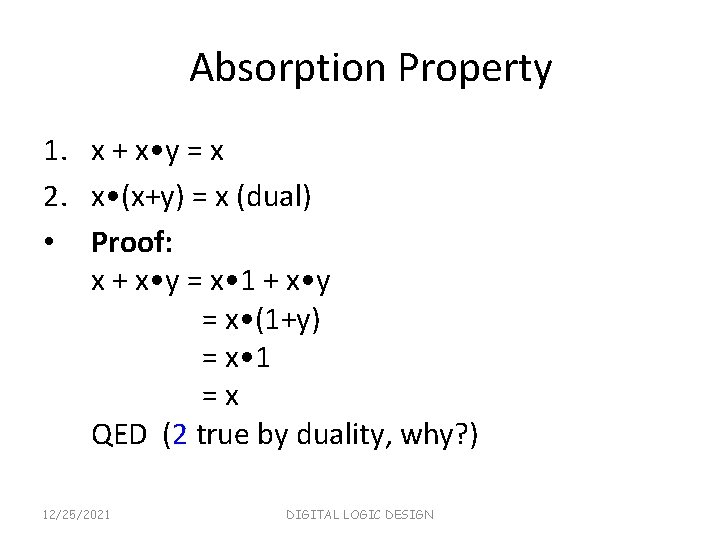
Absorption Property 1. x + x • y = x 2. x • (x+y) = x (dual) • Proof: x + x • y = x • 1 + x • y = x • (1+y) = x • 1 =x QED (2 true by duality, why? ) 12/25/2021 DIGITAL LOGIC DESIGN
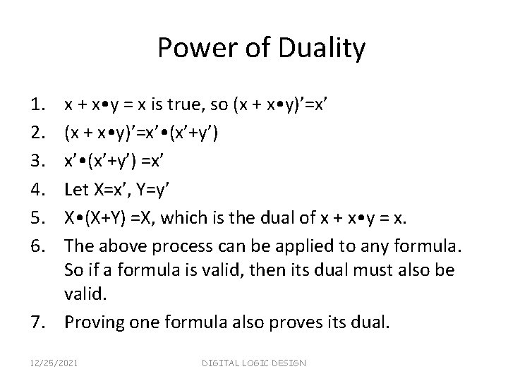
Power of Duality 1. 2. 3. 4. 5. 6. x + x • y = x is true, so (x + x • y)’=x’ • (x’+y’) =x’ Let X=x’, Y=y’ X • (X+Y) =X, which is the dual of x + x • y = x. The above process can be applied to any formula. So if a formula is valid, then its dual must also be valid. 7. Proving one formula also proves its dual. 12/25/2021 DIGITAL LOGIC DESIGN
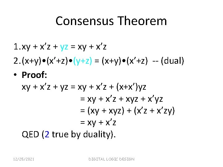
Consensus Theorem 1. xy + x’z + yz = xy + x’z 2. (x+y) • (x’+z) • (y+z) = (x+y) • (x’+z) -- (dual) • Proof: xy + x’z + yz = xy + x’z + (x+x’)yz = xy + x’z + xyz + x’yz = (xy + xyz) + (x’z + x’zy) = xy + x’z QED (2 true by duality). 12/25/2021 DIGITAL LOGIC DESIGN
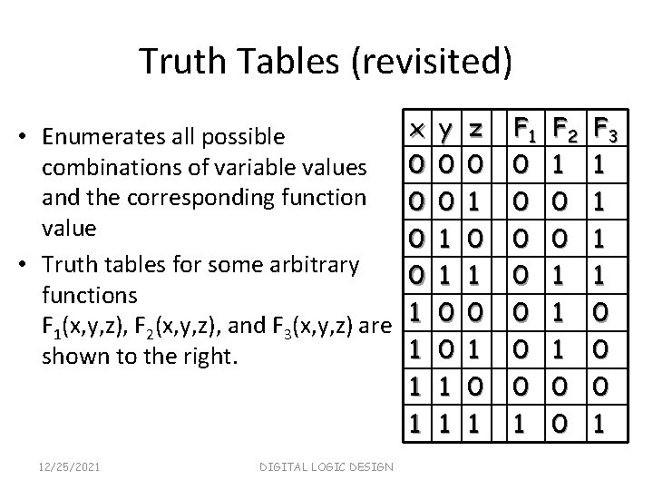
Truth Tables (revisited) • Enumerates all possible combinations of variable values and the corresponding function value • Truth tables for some arbitrary functions F 1(x, y, z), F 2(x, y, z), and F 3(x, y, z) are shown to the right. 12/25/2021 DIGITAL LOGIC DESIGN x 0 0 1 1 y 0 0 1 1 z 0 1 0 1 F 1 0 0 0 0 1 F 2 1 0 0 1 1 1 0 0 F 3 1 1 0 0 0 1
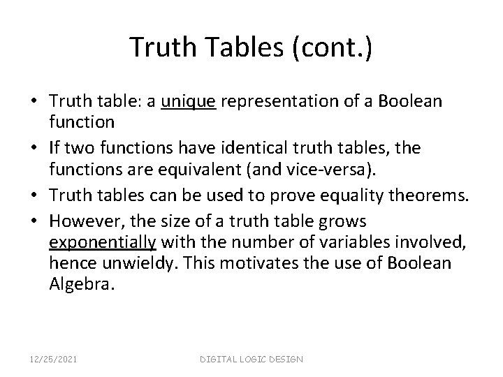
Truth Tables (cont. ) • Truth table: a unique representation of a Boolean function • If two functions have identical truth tables, the functions are equivalent (and vice-versa). • Truth tables can be used to prove equality theorems. • However, the size of a truth table grows exponentially with the number of variables involved, hence unwieldy. This motivates the use of Boolean Algebra. 12/25/2021 DIGITAL LOGIC DESIGN
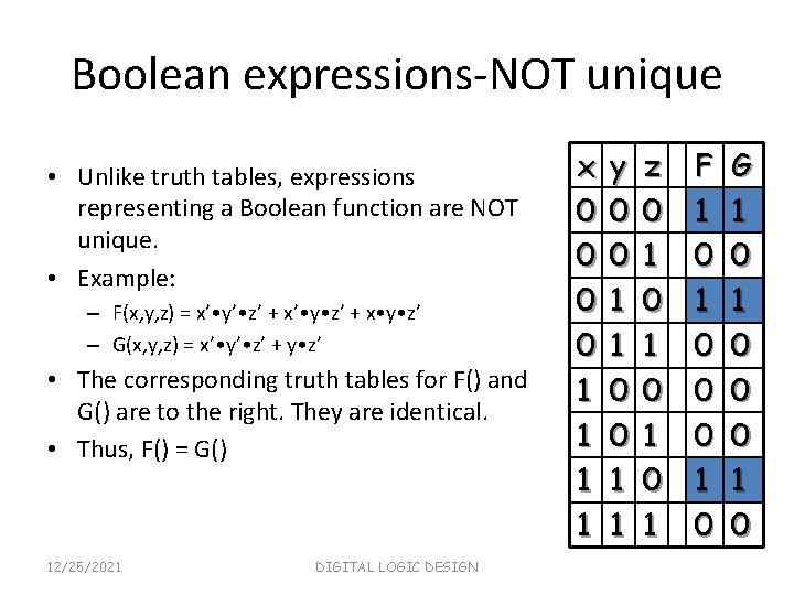
Boolean expressions-NOT unique • Unlike truth tables, expressions representing a Boolean function are NOT unique. • Example: – F(x, y, z) = x’ • y’ • z’ + x’ • y • z’ + x • y • z’ – G(x, y, z) = x’ • y’ • z’ + y • z’ • The corresponding truth tables for F() and G() are to the right. They are identical. • Thus, F() = G() 12/25/2021 DIGITAL LOGIC DESIGN x 0 0 1 1 y 0 0 1 1 z 0 1 0 1 F 1 0 0 0 1 0 G 1 0 0 0 1 0
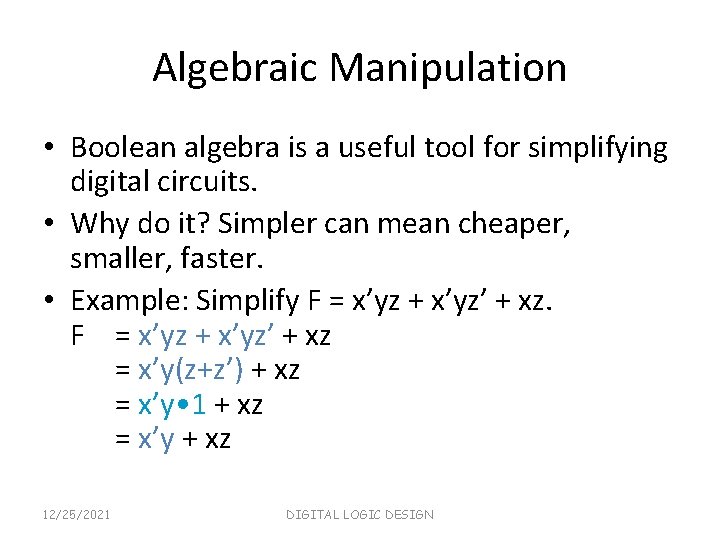
Algebraic Manipulation • Boolean algebra is a useful tool for simplifying digital circuits. • Why do it? Simpler can mean cheaper, smaller, faster. • Example: Simplify F = x’yz + x’yz’ + xz = x’y(z+z’) + xz = x’y • 1 + xz = x’y + xz 12/25/2021 DIGITAL LOGIC DESIGN

Algebraic Manipulation (cont. ) • Example: Prove x’y’z’ + x’yz’ + xyz’ = x’z’ + yz’ • Proof: x’y’z’+ x’yz’+ xyz’ = x’y’z’ + x’yz’ + xyz’ = x’z’(y’+y) + yz’(x’+x) = x’z’ • 1 + yz’ • 1 = x’z’ + yz’ QED. 12/25/2021 DIGITAL LOGIC DESIGN
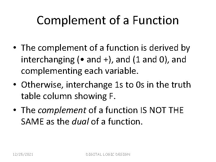
Complement of a Function • The complement of a function is derived by interchanging ( • and +), and (1 and 0), and complementing each variable. • Otherwise, interchange 1 s to 0 s in the truth table column showing F. • The complement of a function IS NOT THE SAME as the dual of a function. 12/25/2021 DIGITAL LOGIC DESIGN
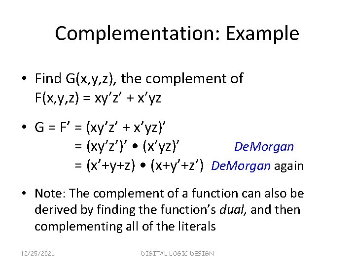
Complementation: Example • Find G(x, y, z), the complement of F(x, y, z) = xy’z’ + x’yz • G = F’ = (xy’z’ + x’yz)’ = (xy’z’)’ • (x’yz)’ De. Morgan = (x’+y+z) • (x+y’+z’) De. Morgan again • Note: The complement of a function can also be derived by finding the function’s dual, and then complementing all of the literals 12/25/2021 DIGITAL LOGIC DESIGN
Canonical and Standard Forms • We need to consider formal techniques for the simplification of Boolean functions. – Identical functions will have exactly the same canonical form. – Minterms and Maxterms – Sum-of-Minterms and Product-of- Maxterms – Product and Sum terms – Sum-of-Products (SOP) and Product-of-Sums (POS) 12/25/2021 DIGITAL LOGIC DESIGN
Definitions Literal: A variable or its complement Product term: literals connected by • Sum term: literals connected by + Minterm: a product term in which all the variables appear exactly once, either complemented or uncomplemented • Maxterm: a sum term in which all the variables appear exactly once, either complemented or uncomplemented • • 12/25/2021 DIGITAL LOGIC DESIGN
Minterm • Represents exactly one combination in the truth table. • Denoted by mj, where j is the decimal equivalent of the minterm’s corresponding binary combination (bj). • A variable in mj is complemented if its value in bj is 0, otherwise is uncomplemented. • Example: Assume 3 variables (A, B, C), and j=3. Then, bj = 011 and its corresponding minterm is denoted by mj = A’BC 12/25/2021 DIGITAL LOGIC DESIGN
Maxterm • Represents exactly one combination in the truth table. • Denoted by Mj, where j is the decimal equivalent of the maxterm’s corresponding binary combination (bj). • A variable in Mj is complemented if its value in bj is 1, otherwise is uncomplemented. • Example: Assume 3 variables (A, B, C), and j=3. Then, bj = 011 and its corresponding maxterm is denoted by Mj = A+B’+C’ 12/25/2021 DIGITAL LOGIC DESIGN

Truth Table notation for Minterms and Maxterms • Minterms and x Maxterms are easy 0 to denote using a 0 truth table. 0 • Example: 0 Assume 3 variables 1 x, y, z 1 (order is fixed) 1 y 1 12/25/2021 z Minterm Maxterm 0 0 x’y’z’ = m 0 x+y+z = M 0 0 1 x’y’z = m 1 x+y+z’ = M 1 1 0 x’yz’ = m 2 x+y’+z = M 2 1 1 x’yz = m 3 x+y’+z’= M 3 0 0 xy’z’ = m 4 x’+y+z = M 4 0 1 xy’z = m 5 x’+y+z’ = M 5 1 0 xyz’ = m 6 x’+y’+z = M 6 1 1 xyz = m 7 x’+y’+z’ = M 7 DIGITAL LOGIC DESIGN
Canonical Forms (Unique) • Any Boolean function F( ) can be expressed as a unique sum of minterms and a unique product of maxterms (under a fixed variable ordering). • In other words, every function F() has two canonical forms: – Canonical Sum-Of-Products (sum of minterms) – Canonical Product-Of-Sums (product of maxterms) 12/25/2021 DIGITAL LOGIC DESIGN
Canonical Forms (cont. ) • Canonical Sum-Of-Products: The minterms included are those mj such that F( ) = 1 in row j of the truth table for F( ). • Canonical Product-Of-Sums: The maxterms included are those Mj such that F( ) = 0 in row j of the truth table for F( ). 12/25/2021 DIGITAL LOGIC DESIGN
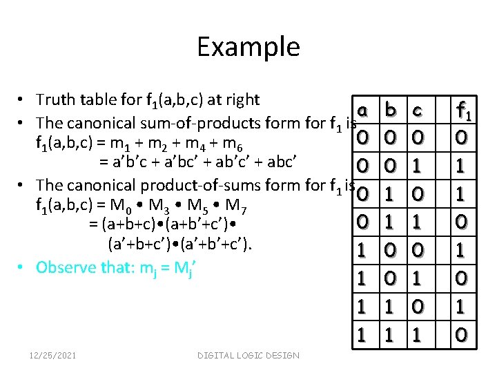
Example • Truth table for f 1(a, b, c) at right a • The canonical sum-of-products form for f 1 is 0 f 1(a, b, c) = m 1 + m 2 + m 4 + m 6 = a’b’c + a’bc’ + ab’c’ + abc’ 0 • The canonical product-of-sums form for f 1 is 0 f 1(a, b, c) = M 0 • M 3 • M 5 • M 7 0 = (a+b+c) • (a+b’+c’) • (a’+b’+c’). 1 • Observe that: mj = Mj’ b 0 0 1 1 12/25/2021 DIGITAL LOGIC DESIGN c 0 1 0 1 f 1 0 1 0 1 0
Shorthand: ∑ and ∏ • f 1(a, b, c) = ∑ m(1, 2, 4, 6), where ∑ indicates that this is a sum-of-products form, and m(1, 2, 4, 6) indicates that the minterms to be included are m 1, m 2, m 4, and m 6. • f 1(a, b, c) = ∏ M(0, 3, 5, 7), where ∏ indicates that this is a product-of-sums form, and M(0, 3, 5, 7) indicates that the maxterms to be included are M 0, M 3, M 5, and M 7. • Since mj = Mj’ for any j, ∑ m(1, 2, 4, 6) = ∏ M(0, 3, 5, 7) = f 1(a, b, c) 12/25/2021 DIGITAL LOGIC DESIGN
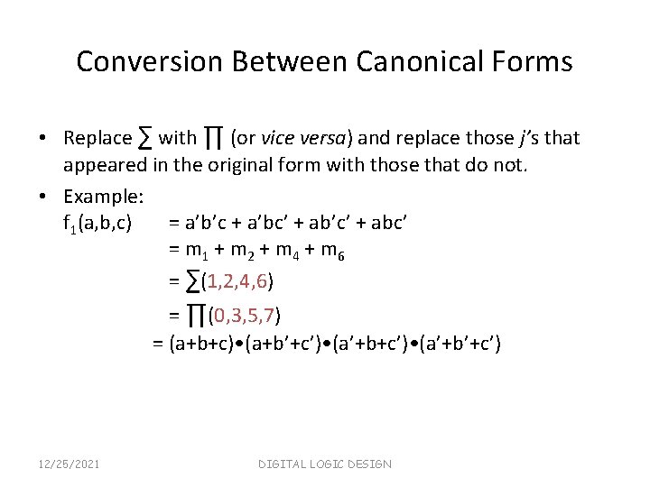
Conversion Between Canonical Forms • Replace ∑ with ∏ (or vice versa) and replace those j’s that appeared in the original form with those that do not. • Example: f 1(a, b, c) = a’b’c + a’bc’ + ab’c’ + abc’ = m 1 + m 2 + m 4 + m 6 = ∑(1, 2, 4, 6) = ∏(0, 3, 5, 7) = (a+b+c) • (a+b’+c’) • (a’+b’+c’) 12/25/2021 DIGITAL LOGIC DESIGN
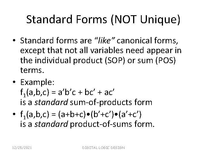
Standard Forms (NOT Unique) • Standard forms are “like” canonical forms, except that not all variables need appear in the individual product (SOP) or sum (POS) terms. • Example: f 1(a, b, c) = a’b’c + bc’ + ac’ is a standard sum-of-products form • f 1(a, b, c) = (a+b+c) • (b’+c’) • (a’+c’) is a standard product-of-sums form. 12/25/2021 DIGITAL LOGIC DESIGN
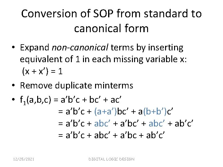
Conversion of SOP from standard to canonical form • Expand non-canonical terms by inserting equivalent of 1 in each missing variable x: (x + x’) = 1 • Remove duplicate minterms • f 1(a, b, c) = a’b’c + bc’ + ac’ = a’b’c + (a+a’)bc’ + a(b+b’)c’ = a’b’c + abc’ + a’bc’ + ab’c’ = a’b’c + abc’ + a’bc + ab’c’ 12/25/2021 DIGITAL LOGIC DESIGN
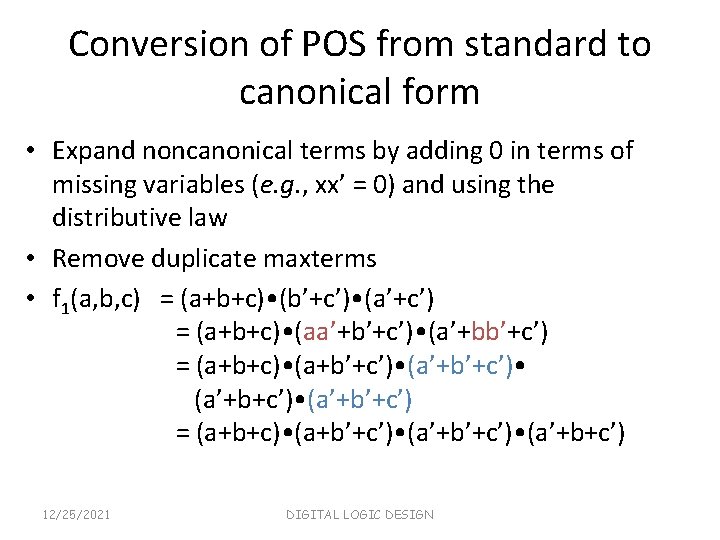
Conversion of POS from standard to canonical form • Expand noncanonical terms by adding 0 in terms of missing variables (e. g. , xx’ = 0) and using the distributive law • Remove duplicate maxterms • f 1(a, b, c) = (a+b+c) • (b’+c’) • (a’+c’) = (a+b+c) • (aa’+b’+c’) • (a’+bb’+c’) = (a+b+c) • (a+b’+c’) • (a’+b+c’) • (a’+b’+c’) = (a+b+c) • (a+b’+c’) • (a’+b+c’) 12/25/2021 DIGITAL LOGIC DESIGN
Karnaugh Maps • Karnaugh maps (K-maps) are graphical representations of boolean functions. • One map cell corresponds to a row in the truth table. • Also, one map cell corresponds to a minterm or a maxterm in the boolean expression • Multiple-cell areas of the map correspond to standard terms. 12/25/2021 DIGITAL LOGIC DESIGN
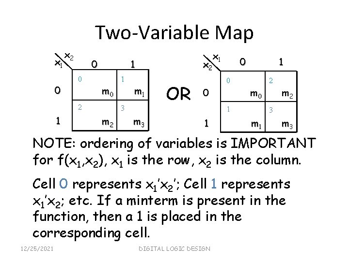
Two-Variable Map x 1 0 x 2 0 1 0 m 1 3 m 2 0 x 2 1 x 1 m 3 OR 1 0 0 2 m 0 1 1 m 2 3 m 1 m 3 NOTE: ordering of variables is IMPORTANT for f(x 1, x 2), x 1 is the row, x 2 is the column. Cell 0 represents x 1’x 2’; Cell 1 represents x 1’x 2; etc. If a minterm is present in the function, then a 1 is placed in the corresponding cell. 12/25/2021 DIGITAL LOGIC DESIGN
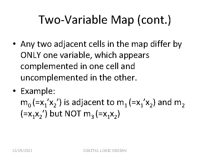
Two-Variable Map (cont. ) • Any two adjacent cells in the map differ by ONLY one variable, which appears complemented in one cell and uncomplemented in the other. • Example: m 0 (=x 1’x 2’) is adjacent to m 1 (=x 1’x 2) and m 2 (=x 1 x 2’) but NOT m 3 (=x 1 x 2) 12/25/2021 DIGITAL LOGIC DESIGN
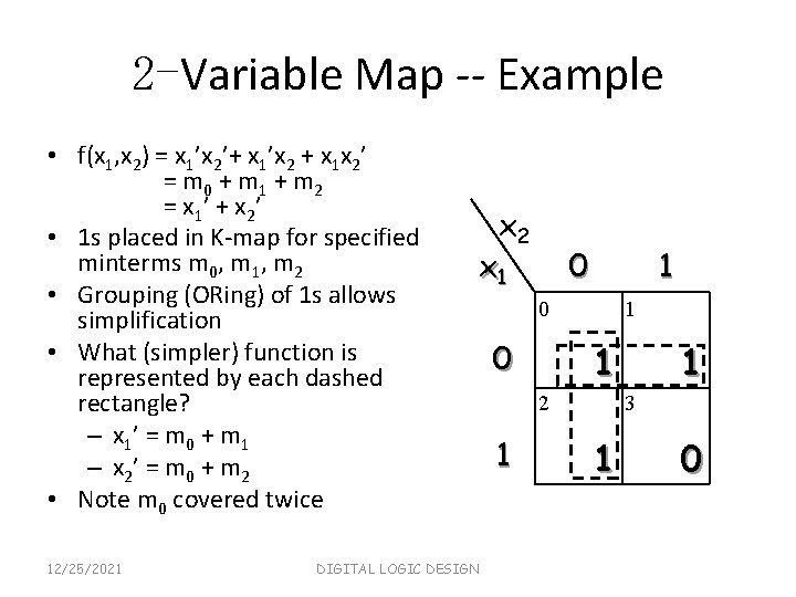
2 -Variable Map -- Example • f(x 1, x 2) = x 1’x 2’+ x 1’x 2 + x 1 x 2’ = m 0 + m 1 + m 2 = x 1’ + x 2’ • 1 s placed in K-map for specified minterms m 0, m 1, m 2 • Grouping (ORing) of 1 s allows simplification • What (simpler) function is represented by each dashed rectangle? – x 1 ’ = m 0 + m 1 – x 2 ’ = m 0 + m 2 • Note m 0 covered twice 12/25/2021 x 2 x 1 DIGITAL LOGIC DESIGN 0 1 0 0 1 1 2 1 1 3 1 0
Minimization as SOP using K-map • Enter 1 s in the K-map for each product term in the function • Group adjacent K-map cells containing 1 s to obtain a product with fewer variables. Group size must be in power of 2 (2, 4, 8, …) • Handle “boundary wrap” for K-maps of 3 or more variables. • Realize that answer may not be unique 12/25/2021 DIGITAL LOGIC DESIGN

Three-Variable Map yz 00 x 0 0 1 m 0 4 1 01 3 m 1 5 m 4 11 2 m 3 7 m 5 10 m 2 6 m 7 m 6 -Note: variable ordering is (x, y, z); yz specifies column, x specifies row. -Each cell is adjacent to three other cells (left or right or top or bottom or edge wrap) 12/25/2021 DIGITAL LOGIC DESIGN
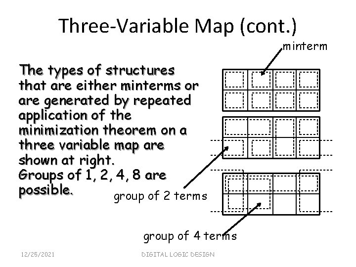
Three-Variable Map (cont. ) minterm The types of structures that are either minterms or are generated by repeated application of the minimization theorem on a three variable map are shown at right. Groups of 1, 2, 4, 8 are possible. group of 2 terms group of 4 terms 12/25/2021 DIGITAL LOGIC DESIGN
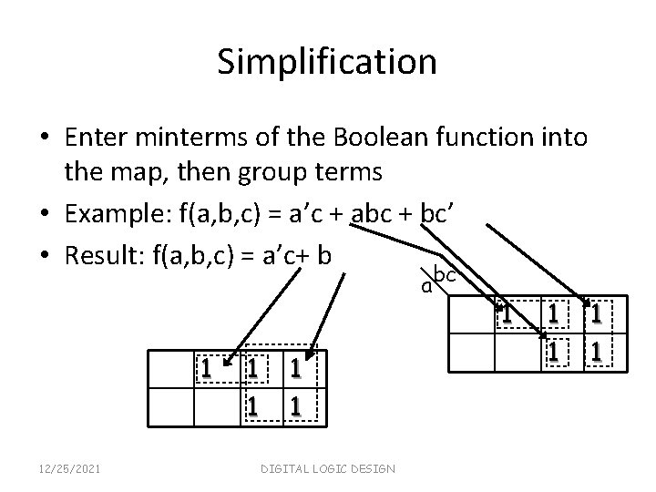
Simplification • Enter minterms of the Boolean function into the map, then group terms • Example: f(a, b, c) = a’c + abc + bc’ • Result: f(a, b, c) = a’c+ b a bc 1 12/25/2021 1 1 DIGITAL LOGIC DESIGN 1 1 1
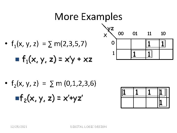
More Examples X • f 1(x, y, z) = ∑ m(2, 3, 5, 7) n f 1(x, y, z) = x’y + xz • f 2(x, y, z) = ∑ m (0, 1, 2, 3, 6) nf 2(x, 12/25/2021 y, z) = x’+yz’ DIGITAL LOGIC DESIGN yz 00 01 11 10 1 1 1 1 0 1 1 1

Four-Variable Maps YZ WX 00 01 11 10 00 m 1 m 3 m 2 01 m 4 m 5 m 7 m 6 11 m 12 m 13 m 15 m 14 10 m 8 m 9 m 11 m 10 • Top cells are adjacent to bottom cells. Left-edge cells are adjacent to right-edge cells. • Note variable ordering (WXYZ). 12/25/2021 DIGITAL LOGIC DESIGN
Four-variable Map Simplification • One square represents a minterm of 4 literals. • A rectangle of 2 adjacent squares represents a product term of 3 literals. • A rectangle of 4 squares represents a product term of 2 literals. • A rectangle of 8 squares represents a product term of 1 literal. • A rectangle of 16 squares produces a function that is equal to logic 1. 12/25/2021 DIGITAL LOGIC DESIGN
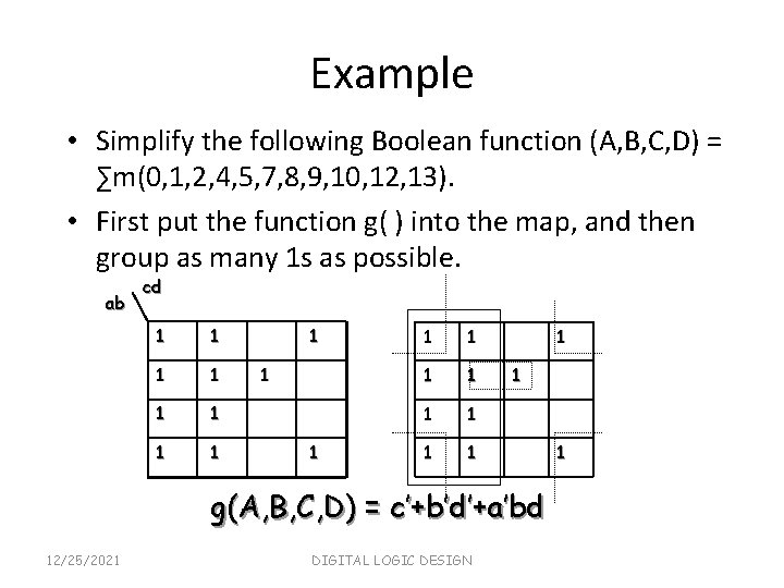
Example • Simplify the following Boolean function (A, B, C, D) = ∑m(0, 1, 2, 4, 5, 7, 8, 9, 10, 12, 13). • First put the function g( ) into the map, and then group as many 1 s as possible. ab cd 1 1 1 1 1 1 g(A, B, C, D) = c’+b’d’+a’bd 12/25/2021 DIGITAL LOGIC DESIGN 1
Don't Care Conditions • There may be a combination of input values which – will never occur – if they do occur, the output is of no concern. • The function value for such combinations is called a don't care. • They are denoted with x or –. Each x may be arbitrarily assigned the value 0 or 1 in an implementation. • Don’t cares can be used to further simplify a function 12/25/2021 DIGITAL LOGIC DESIGN
Minimization using Don’t Cares • Treat don't cares as if they are 1 s to generate PIs. • Delete PI's that cover only don't care minterms. • Treat the covering of remaining don't care minterms as optional in the selection process (i. e. they may be, but need not be, covered). 12/25/2021 DIGITAL LOGIC DESIGN
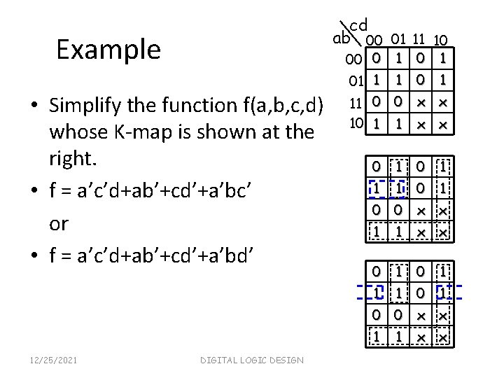
cd ab 00 01 11 10 Example • Simplify the function f(a, b, c, d) whose K-map is shown at the right. • f = a’c’d+ab’+cd’+a’bc’ or • f = a’c’d+ab’+cd’+a’bd’ 00 0 1 01 1 1 0 1 11 0 0 x x 10 1 1 x x 0 1 0 1 1 1 0 1 0 0 x x 1 12/25/2021 DIGITAL LOGIC DESIGN 1 x x
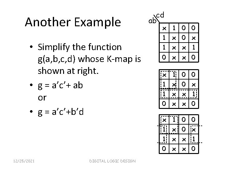
Another Example • Simplify the function g(a, b, c, d) whose K-map is shown at right. • g = a’c’+ ab or • g = a’c’+b’d cd ab x 1 0 0 1 x 0 x 1 x x 1 0 x x 0 12/25/2021 DIGITAL LOGIC DESIGN
Algorithmic minimization • What do we do for functions with more variables? • You can “code up” a minimizer (Computer. Aided Design, CAD) – Quine-Mc. Cluskey algorithm – Iterated consensus • We won’t discuss these techniques here 12/25/2021 DIGITAL LOGIC DESIGN
More Logic Gates ((Universal Gates) • NAND and NOR Gates – NAND and NOR circuits – Two-level Implementations – Multilevel Implementations • Exclusive-OR (XOR) Gates – Odd Function – Parity Generation and Checking 12/25/2021 DIGITAL LOGIC DESIGN
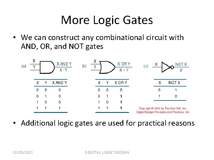
More Logic Gates • We can construct any combinational circuit with AND, OR, and NOT gates • Additional logic gates are used for practical reasons 12/25/2021 DIGITAL LOGIC DESIGN
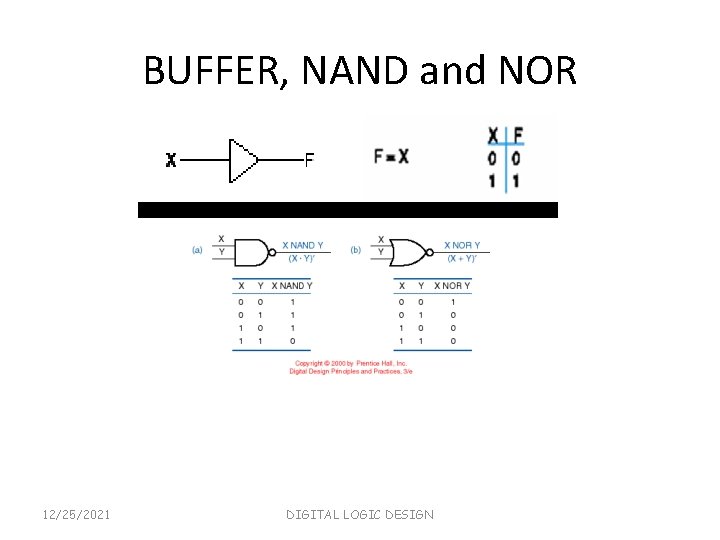
BUFFER, NAND and NOR 12/25/2021 DIGITAL LOGIC DESIGN
NAND Gate • Known as a “universal” gate because ANY digital circuit can be implemented with NAND gates alone. • To prove the above, it suffices to show that AND, OR, and NOT can be implemented using NAND gates only. 12/25/2021 DIGITAL LOGIC DESIGN
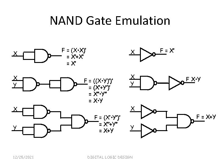
NAND Gate Emulation X X Y F = (X • X)’ = X’+X’ = X’ X F = ((X • Y)’)’ = (X’+Y’)’ = X’’ • Y’’ = X • Y 12/25/2021 F X • Y X X Y F = X’ F = (X’ • Y’)’ = X’’+Y’’ = X+Y F = X+Y Y DIGITAL LOGIC DESIGN
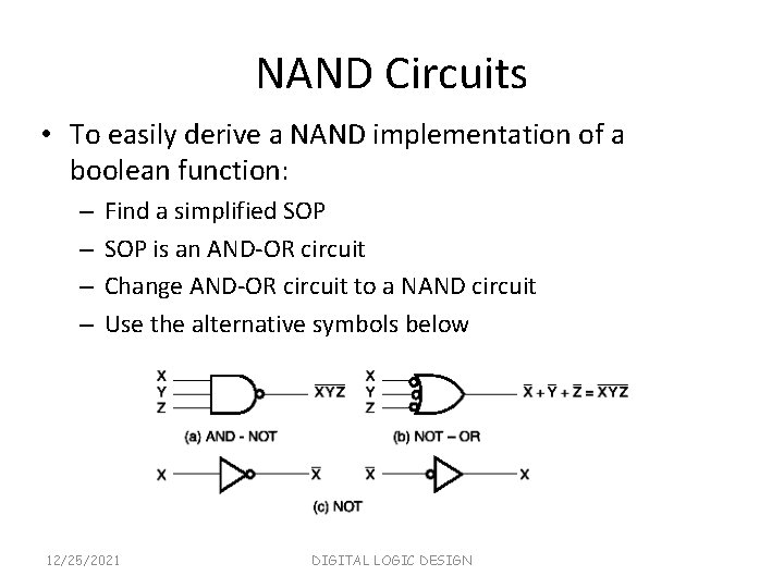
NAND Circuits • To easily derive a NAND implementation of a boolean function: – – Find a simplified SOP is an AND-OR circuit Change AND-OR circuit to a NAND circuit Use the alternative symbols below 12/25/2021 DIGITAL LOGIC DESIGN
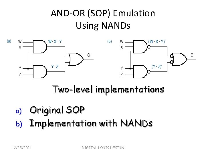
AND-OR (SOP) Emulation Using NANDs Two-level implementations a) b) Original SOP Implementation with NANDs 12/25/2021 DIGITAL LOGIC DESIGN
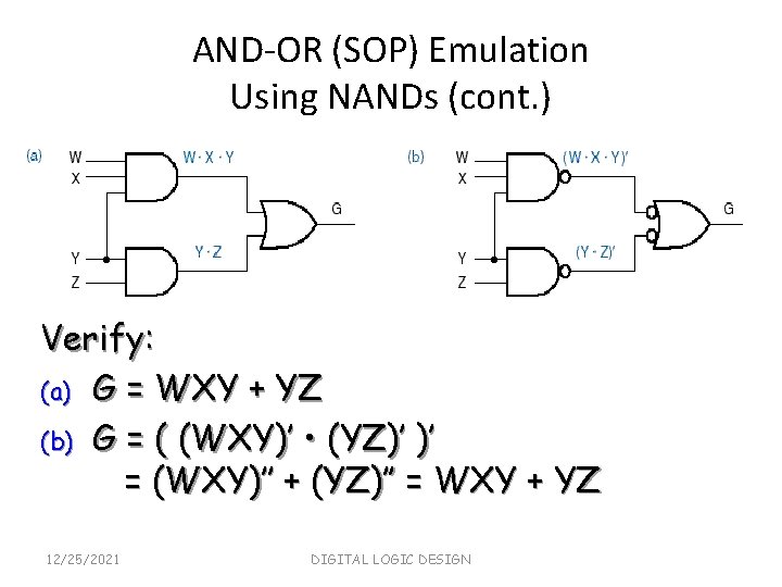
AND-OR (SOP) Emulation Using NANDs (cont. ) Verify: (a) G = WXY + YZ (b) G = ( (WXY)’ • (YZ)’ )’ = (WXY)’’ + (YZ)’’ = WXY + YZ 12/25/2021 DIGITAL LOGIC DESIGN
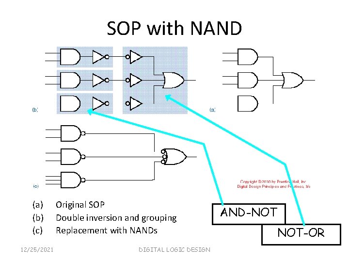
SOP with NAND (a) (b) (c) 12/25/2021 Original SOP Double inversion and grouping Replacement with NANDs DIGITAL LOGIC DESIGN AND-NOT NOT-OR
Two-Level NAND Gate Implementation - Example F (X, Y, Z) = m(0, 6) 1. Express F in SOP form: F = X’Y’Z’ + XYZ’ 2. Obtain the AND-OR implementation for F. 3. Add bubbles and inverters to transform AND-OR to NAND-NAND gates. 12/25/2021 DIGITAL LOGIC DESIGN
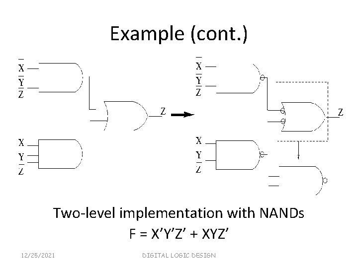
Example (cont. ) Two-level implementation with NANDs F = X’Y’Z’ + XYZ’ 12/25/2021 DIGITAL LOGIC DESIGN
Multilevel NAND Circuits Starting from a multilevel circuit: 1. Convert all AND gates to NAND gates with ANDNOT graphic symbols. 2. Convert all OR gates to NAND gates with NOT-OR graphic symbols. 3. Check all the bubbles in the diagram. For every bubble that is not counteracted by another bubble along the same line, insert a NOT gate or complement the input literal from its original appearance. 12/25/2021 DIGITAL LOGIC DESIGN
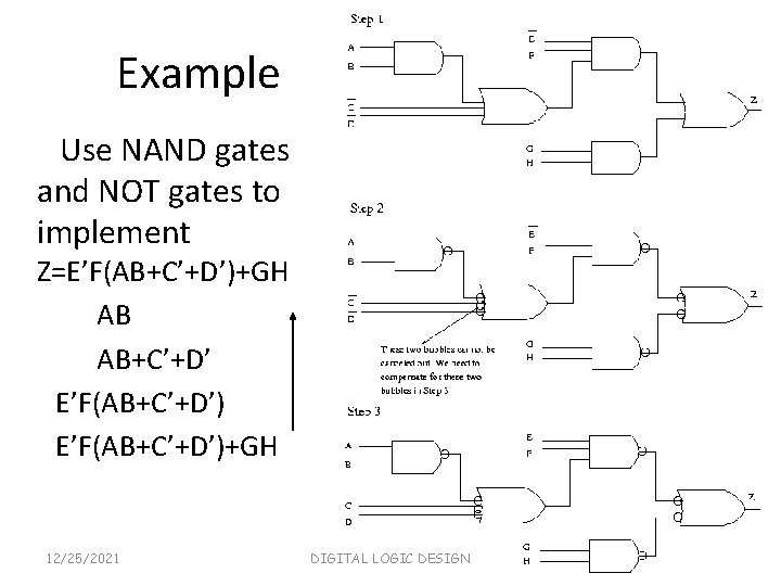
Example Use NAND gates and NOT gates to implement Z=E’F(AB+C’+D’)+GH AB AB+C’+D’ E’F(AB+C’+D’)+GH 12/25/2021 DIGITAL LOGIC DESIGN
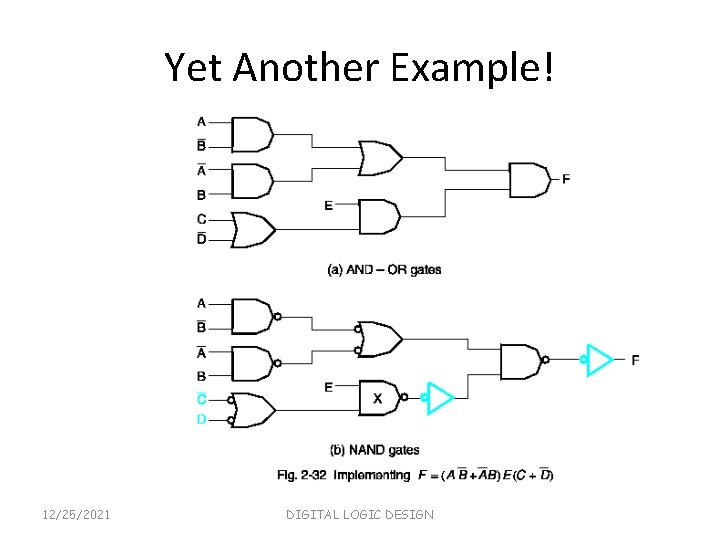
Yet Another Example! 12/25/2021 DIGITAL LOGIC DESIGN
NOR Gate • Also a “universal” gate because ANY digital circuit can be implemented with NOR gates alone. • This can be similarly proven as with the NAND gate. 12/25/2021 DIGITAL LOGIC DESIGN
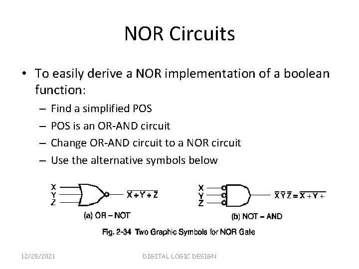
NOR Circuits • To easily derive a NOR implementation of a boolean function: – – Find a simplified POS is an OR-AND circuit Change OR-AND circuit to a NOR circuit Use the alternative symbols below 12/25/2021 DIGITAL LOGIC DESIGN
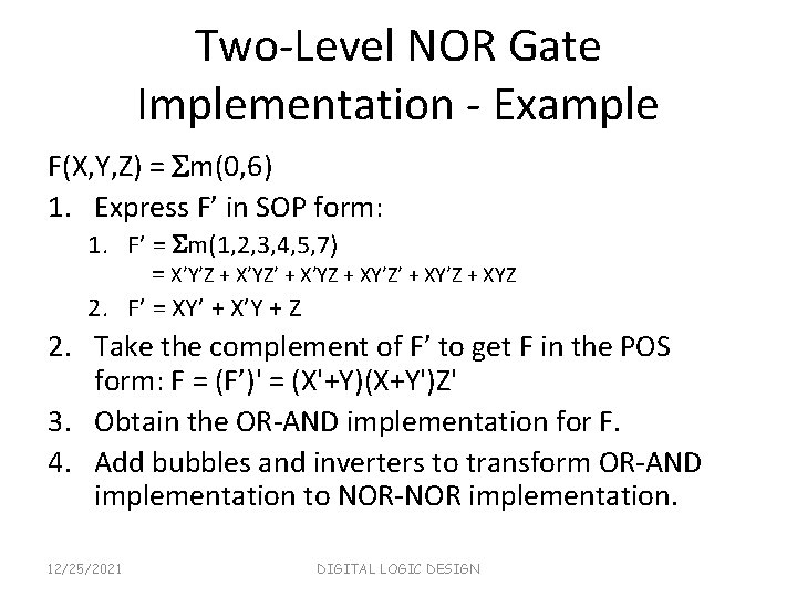
Two-Level NOR Gate Implementation - Example F(X, Y, Z) = m(0, 6) 1. Express F’ in SOP form: 1. F’ = m(1, 2, 3, 4, 5, 7) = X’Y’Z + X’YZ’ + X’YZ + XY’Z’ + XY’Z + XYZ 2. F’ = XY’ + X’Y + Z 2. Take the complement of F’ to get F in the POS form: F = (F’)' = (X'+Y)(X+Y')Z' 3. Obtain the OR-AND implementation for F. 4. Add bubbles and inverters to transform OR-AND implementation to NOR-NOR implementation. 12/25/2021 DIGITAL LOGIC DESIGN
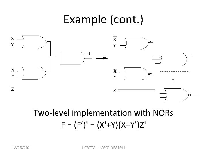
Example (cont. ) Two-level implementation with NORs F = (F’)' = (X'+Y)(X+Y')Z' 12/25/2021 DIGITAL LOGIC DESIGN
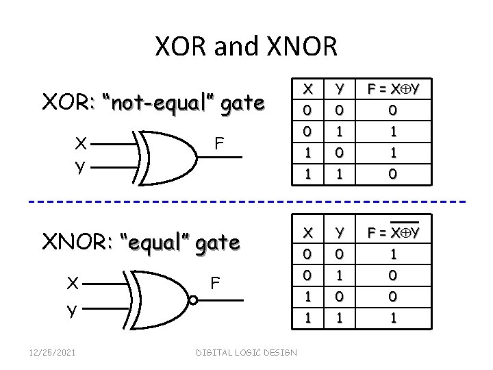
XOR and XNOR XOR: “not-equal” gate X Y F XNOR: “equal” gate X F Y 12/25/2021 DIGITAL LOGIC DESIGN X Y F = X Y 0 0 1 1 1 0 X Y F = X Y 0 0 1 0 1 0 0 1 1 1
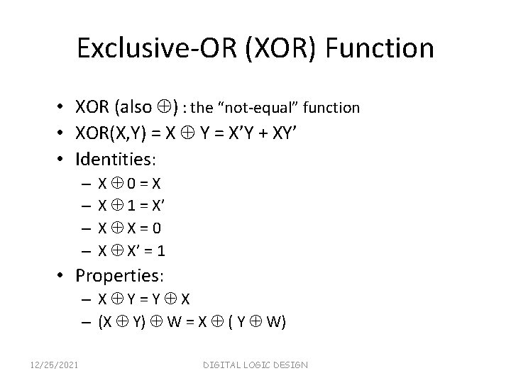
Exclusive-OR (XOR) Function • XOR (also ) : the “not-equal” function • XOR(X, Y) = X Y = X’Y + XY’ • Identities: – – X 0=X X 1 = X’ X X=0 X X’ = 1 • Properties: – X Y=Y X – (X Y) W = X ( Y W) 12/25/2021 DIGITAL LOGIC DESIGN
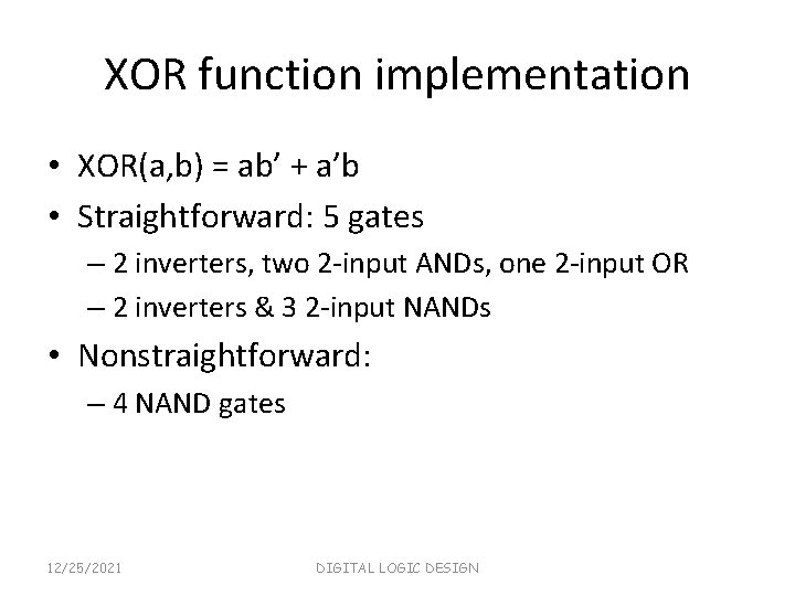
XOR function implementation • XOR(a, b) = ab’ + a’b • Straightforward: 5 gates – 2 inverters, two 2 -input ANDs, one 2 -input OR – 2 inverters & 3 2 -input NANDs • Nonstraightforward: – 4 NAND gates 12/25/2021 DIGITAL LOGIC DESIGN
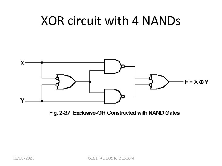
XOR circuit with 4 NANDs 12/25/2021 DIGITAL LOGIC DESIGN
References Ø https: //www. geeksforgeeks. org/digital-electronics-logic-design-tutorials/ Ø Digital Logic And Computer Design By M. Morris Mano, 2004. 12/25/2021 DIGITAL LOGIC DESIGN
- Slides: 83