
Bandgap Current Reference source FEI 4ACREF Vladimir Gromov
Bandgap Current Reference source: FEI 4_A_CREF Vladimir Gromov NIKHEF, Amsterdam, the Netherlands FEI 4 collaboration. November 29, 2009.

The system requirements An extract from the document called “ Minutes-nov-11. pdf”, distributed by Maurice Garcia-Sciveres by E-mail on November 11 2009 (19: 25) 22) The trim bits of the current reference will be modified to provide adjustment between nominal-30% and nominal+30%. Adjustment should only be possible in this narrow range. Setting the trim bits to 0 should not shut off the CREF, but simply set it to nominal-30%. 30% is not an exact requirement, could be 35% or 40% or 25% or something of that order. Subject: Re: CREF From: Abderrezak Mekkaoui <amekkaoui@lbl. gov> Date: Wed, 11 Nov 2009 10: 18: 06 -0800 To: <r. kluit@nikhef. nl>, "ATLAS Pixel B-layer Replacement Electronics" <atlas-pixel-blr-electronics@cern. ch> Hi Vladimir/Ruud, The nominal is whatever you think the "optimal" should be based on the design (2. 7 u. A according to the last year simulations). If it is 2 u. A then no problem. The only thing is that tuning should be done around the nominal value (not from 0 to max). ± 1% (after tuning) would be very nice. ± 5% acceptable. I hope this helps. Abderrezak On 11/11/2009 7: 10 AM, Ruud Kluit wrote: Hello Abderrezak, Vladimir. G is busy doing the IC 5 > IC 6 cerversion of the CREF. During a recent (14 th Oct. ) phone meeting you mentioned that 2 u. A is the value as default for the CREF output. The tuning should be made such that all process corners can be tuned back to 2 u. A. This is what Vladimir did now. During the review you said 2. 7 u. A. . . So, you should be aware that the design is now optimized for 2 u. A. Regards, Ruud. FEI 4 collaboration V. Gromov 29/11/09 2
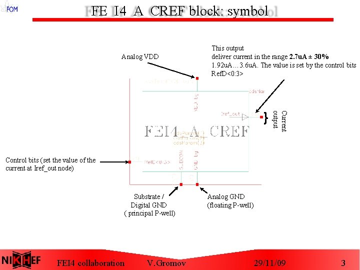
FE_I 4_A_CREF block: symbol Analog VDD This output deliver current in the range 2. 7 u. A ± 30% 1. 92 u. A… 3. 6 u. A. The value is set by the control bits Ref. D<0: 3> Current output Control bits (set the value of the current at Iref_out node) Substrate / Digital GND ( principal P-well) FEI 4 collaboration V. Gromov Analog GND (floating P-well) 29/11/09 3
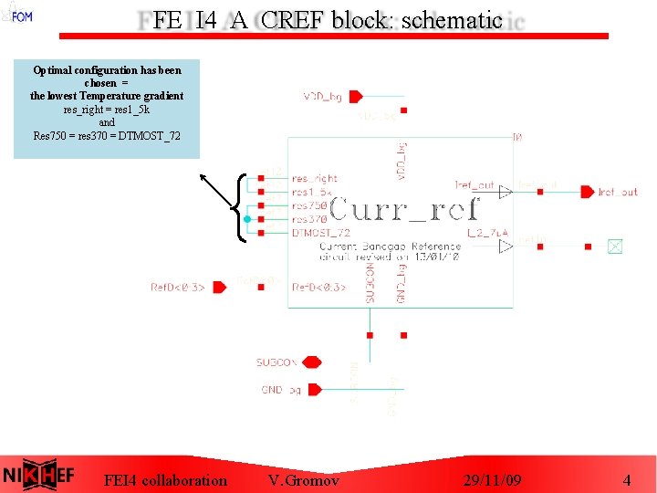
FE_I 4_A_CREF block: schematic Optimal configuration has been chosen = the lowest Temperature gradient res_right = res 1_5 k and Res 750 = res 370 = DTMOST_72 FEI 4 collaboration V. Gromov 29/11/09 4
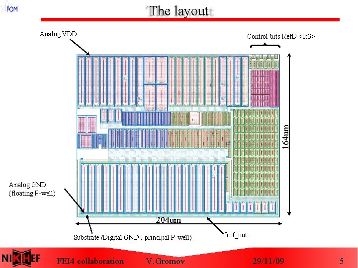
The layout Analog VDD 164 um Control bits Ref. D <0: 3> Analog GND (floating P-well) 204 um Substrate /Digital GND ( principal P-well) FEI 4 collaboration V. Gromov Iref_out 29/11/09 5
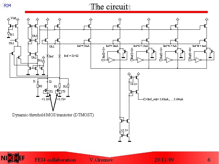
The circuit Vdd Ub 2 Iref = I 1+I 2 Iref*= 26 u. A Iref*/2 = 15 u. A Ib 2 I 1 I 2 R 1 T 1 <1: 18> Iref*/4 = 7 u. A Ref. D<0> Iref*= 52 u. A Ub 1 Ref. D<2> Ub 1 Ref. D<1> Ub 3 Ref. D<3> Ib 1 Iref*/8 = 3 u. A <6: 1> R 2 T 2 <1: 72> Iref_out= 1. 92 u. A, … 3. 66 u. A Dynamic-threshold MOS transistor (DTMOST) <5: 1> FEI 4 collaboration V. Gromov 29/11/09 6
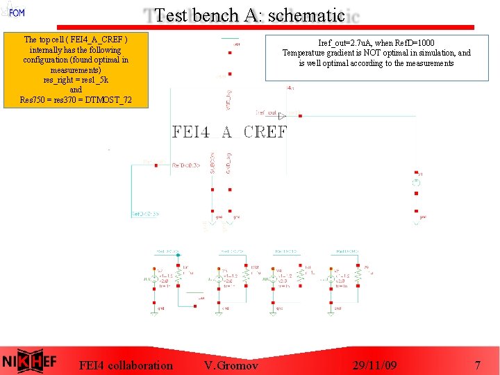
Test bench A: schematic The top cell ( FEI 4_A_CREF ) internally has the following configuration (found optimal in measurements) res_right = res 1_5 k and Res 750 = res 370 = DTMOST_72 Iref_out=2. 7 u. A, when Ref. D=1000 Temperature gradient is NOT optimal in simulation, and is well optimal according to the measurements Curr_ref FEI 4 collaboration V. Gromov 29/11/09 7
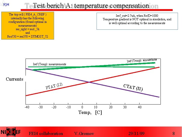
Test bench A: temperature compensation The top cell ( FEI 4_A_CREF ) internally has the following configuration (found optimal in measurements) res_right = res 1_5 k and Res 750 = res 370 = DTMOST_72 Iref_out=2. 7 u. A, when Ref. D=1000 Temperature gradient is NOT optimal in simulation, and is well optimal according to the measurements Iref (Temp): simul Iref (Temp): measurements ations Currents PTAT -40 -30 (I 2) -20 CTAT -10 0 10 20 30 (I 1) 40 Temp, [C] FEI 4 collaboration V. Gromov 29/11/09 8
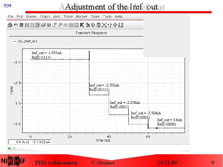
Adjustment of the Iref_out = -1. 935 u. A Ref. D (1111) Iref_out = -2. 792 u. A Ref. D (0111) Iref_out = -3. 274 u. A Ref. D (0011) Iref_out = -3. 504 u. A Ref. D (0001) Iref_out = 3. 6 u. A Ref. D (0000) FEI 4 collaboration V. Gromov 29/11/09 9
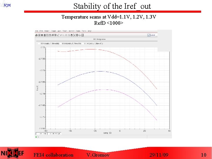
Stability of the Iref_out Temperature scans at Vdd=1. 1 V, 1. 2 V, 1. 3 V Ref. D <1000> FEI 4 collaboration V. Gromov 29/11/09 10
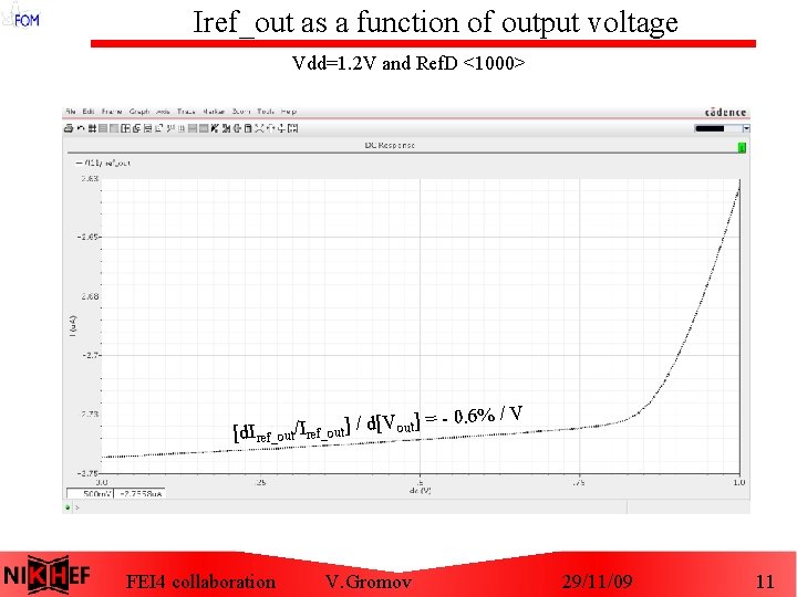
Iref_out as a function of output voltage Vdd=1. 2 V and Ref. D <1000> - 0. 6% / V = ] [V d / ] t ou out/Iref_out [d. Iref_ FEI 4 collaboration V. Gromov 29/11/09 11
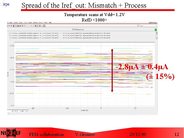
Spread of the Iref_out: Mismatch + Process Temperature scans at Vdd= 1. 2 V Ref. D <1000> -2. 8μA ± 0. 4μA (± 15%) FEI 4 collaboration V. Gromov 29/11/09 12
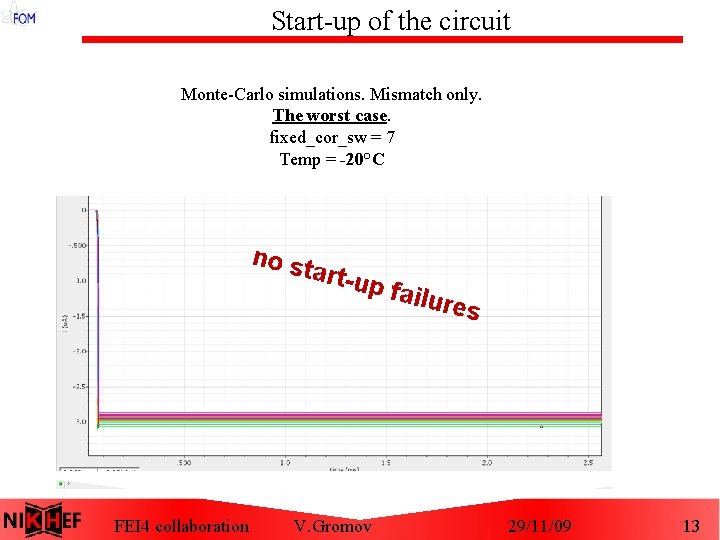
Start-up of the circuit Monte-Carlo simulations. Mismatch only. The worst case. fixed_cor_sw = 7 Temp = -20°C no st art-u FEI 4 collaboration p fail V. Gromov ures 29/11/09 13
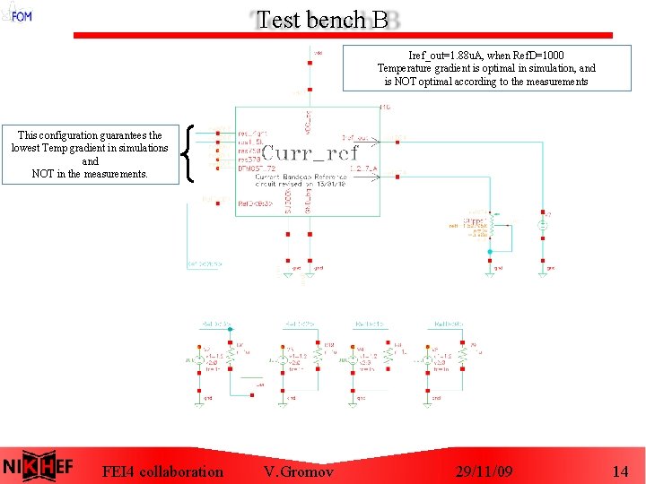
Test bench B Iref_out=1. 88 u. A, when Ref. D=1000 Temperature gradient is optimal in simulation, and is NOT optimal according to the measurements This configuration guarantees the lowest Temp gradient in simulations and NOT in the measurements. FEI 4 collaboration V. Gromov 29/11/09 14

Lessons learned - when two adjustent cell have substrate connection RX+BP+CA+M 1 (sub net) use SXCUT to run Assura LVS -do not use GRLOGIC as long as it masks GR 110 a (RX overlap past PC - silicide width) > 0. 55 u) - Use approapriate shapes when drawing PC in all gate around geometry. The cut must exclude corners<45°. Put an extra shape on it. -put more metal on VDD bus in order to avoid GR 594 (For nets connected to NW contact, where the NW net is not connected to a substrate contact defined by ((RX over BP) not over (NW or RN or BB or JD or PI or T 3)), the ratio of [ (20*Mx area) + (Non-isolated p+ junction area ((((RX over BP) over NW) not over PC) not over T 3)) ] / (union[NW, PI] area) where x=1, 2, 3, 4, 5, 6. ) - Change size of the Bbox by editing rectangular in the layer chng. Lyr t 0 - use layer called LVS: drawing 1 in order to define triple well NFETs (nfettw) devices in layout - Please re-attach IBM library properties* to match current metal stack (it is now set at "6 -2" instead of "3 -2" and another property is missing): use menu item CIW>IBM_PDK>Library>Add IBM_PDK Lib Properties. -In fact it does not work like this. You need to check out (from the repository) file called data. dm - There is a no. Conn cell that should probably point to 'basic' cadence library rather then to your own lib. - Several cellnames contain a '. ' character, which is an issue in Calibre but only when checking those cells as top cells - so don't bother fixing this. - to run DRC check in Calibre: -setting: BEOL_STACK = 3_2_3, TECHDIR = /user/foundry/vlsi/IBM/cmos 8 sf/IBM_PDK/rel. DM/Calibre -BURN_IN=empty, CHECK_RECOMENDED=ON, DENSITY_LOCAL=ON, DESIGN_TYPE=CELL, EXT_LATCHUP =JEDEC 78, IOTYPE=WB_INLINE -use the following runset /project/et/Atlas/Upgrade/Inner. Tracker/Pixel. Det/cadence/FE_I 4_bandgap/vgromov_05_01_10. drc, - to run LVS check in Calibre: -Setting: COMPARE_NF_VALUES=FALSE, LASTMETAL=MA, MGPROCESS=MG, NO_SUBC_IN_GRLOGIC=TRUE, NO_TRACE_PROPERTY=FALSE, NUMMETAL=8, PEX_RUN=FALSE, PWELL_SUBC_DEVICE=FALSE, USE_RESISTANCE_MULTIPLIERS=TRUE. -use the following runset -/project/et/Atlas/Upgrade/Inner. Tracker/Pixel. Det/cadence/FE_I 4_bandgap/lvs_gromov_06_01_10. runset -this runset generate all the netlist files when choose: Export from layout viewer=ON and Export from schematic viewer=ON FEI 4 collaboration V. Gromov 29/11/09 15

Lessons learned -RULE FILE: /project/et/Atlas/Upgrade/Inner. Tracker/Pixel. Det/cadence/FE_I 4_bandgap/Calibre. LVS/_cmrf 8 sf. lvs. cal_ -Check LVS setting in : /project/et/Atlas/Upgrade/Inner. Tracker/Pixel. Det/cadence/FE_I 4_bandgap/example. lvs. report -When parallel MOST’s are not of the same size they will be seen as two different devices in layout and as one device in schematic. This causes LVS discrepancy. Put resistors (opndres_inh) in series with the gate connection in order to make two device in schematic too. This will solve the problem. - put two labels in sub. drw and SXCUT. lbl layer in order to stamp the substrate with nothing under Connectivity>Net name (assigns name sub! to substrate) -in schematic use nfet_inh devices when you want to give the name sub! to the substrate. - use subc component : put SUBCON net name on the net connected to SUBCON pin and inherited name on the net connected to the sub pin as follows: - Add Wire Name> Net Expression> Property Name = substrate and Default Net Name = sub! (then the global net sub! will be present in all the blocks and no dedicate pin is needed in schematic only) -Put a note on the symbol view to order to make it clear which cell is this (use Create>Note>Text> Font. Height=0. 2, Font Style=roman do not forget that the value of the output current will be 40% higher when you change the setting from res_right = res 1_5 k (optimal operational point in simulations) to res_right = res 1_5 k + Res 750 = res 370 = DTMOST_72 (optimal point found in the measurements) Take it into account when you calculate the size ratio in the current mirrors. if res_right = res 1_5 k then Iout_largest = 26. 11 u. A in simulation and 30. 3 u. A in the measurements if res_right = res 1_5 k + Res 750 = res 370 = DTMOST_72 then Iout_largest = 39. 79 u. A in simulation and 43. 7 u. A in the measurements - FEI 4 collaboration V. Gromov 29/11/09 16
- Slides: 16