
b a 1 Fig 1 Kuo et al
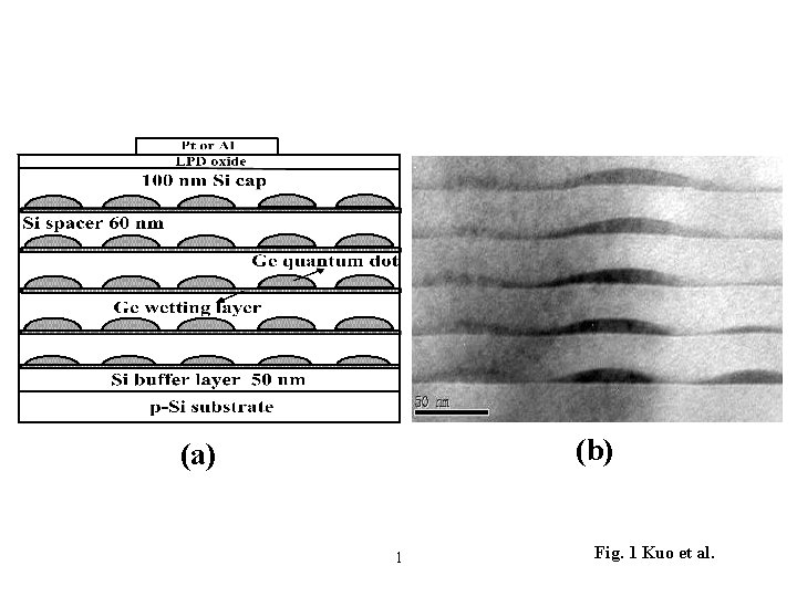
(b) (a) 1 Fig. 1 Kuo et al.
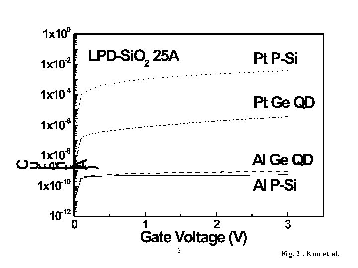
2 Fig. 2. Kuo et al.
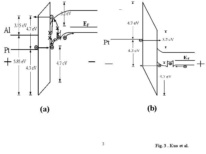
(b) (a) 3 Fig. 3. Kuo et al.
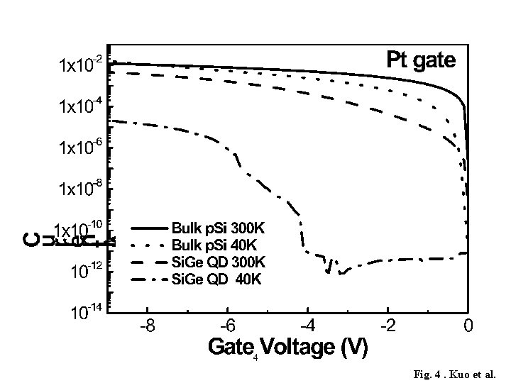
4 Fig. 4. Kuo et al.
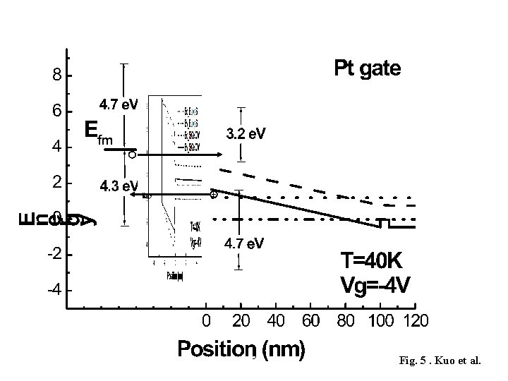
5 Fig. 5. Kuo et al.
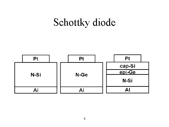
Schottky diode 6
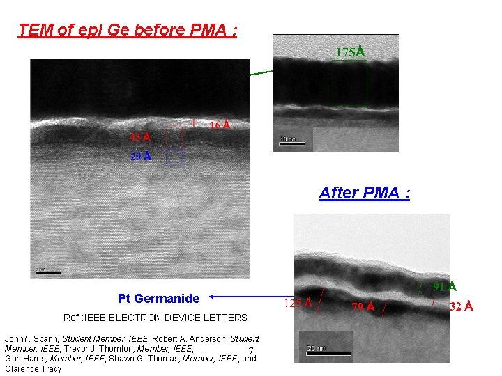
TEM of epi Ge before PMA : After PMA : Pt Germanide Ref : IEEE ELECTRON DEVICE LETTERS John. Y. Spann, Student Member, IEEE, Robert A. Anderson, Student Member, IEEE, Trevor J. Thornton, Member, IEEE, 7 Gari Harris, Member, IEEE, Shawn G. Thomas, Member, IEEE, and Clarence Tracy
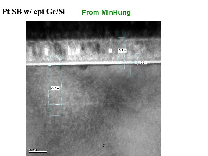
Pt SB w/ epi Ge/Si From Min. Hung 8
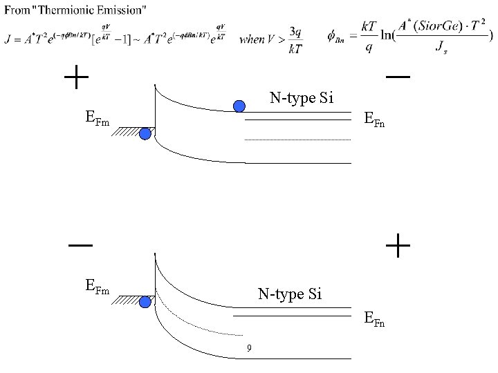
N-type Si EFm EFn EFm N-type Si EFn 9
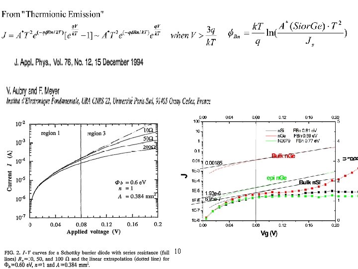
10
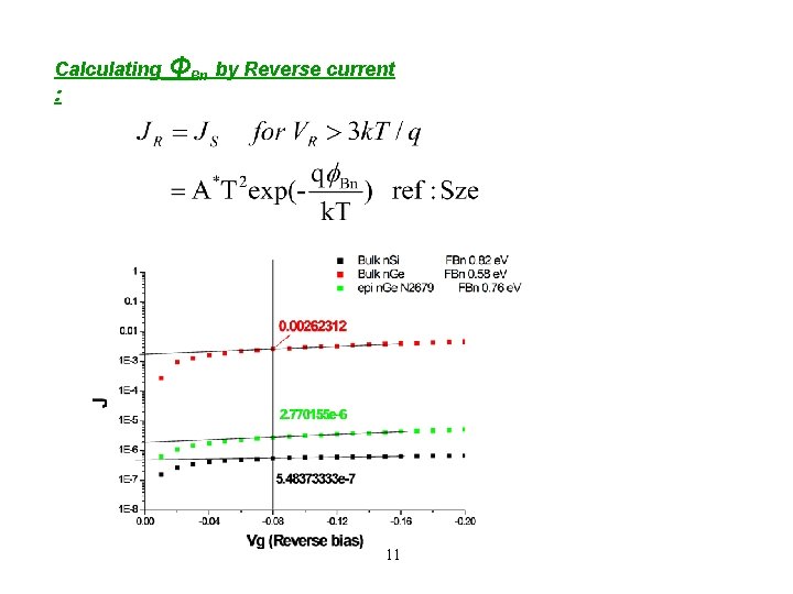
Calculating : ΦBn by Reverse current 11
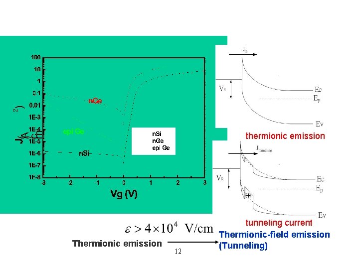
I-V curves thermionic emission Thermionic emission 12 tunneling current Thermionic-field emission (Tunneling)

Thermionic-field emission (Tunneling) Thermionic emission From Simulation : n. Si E-field~ 2 e 4 V/cm Epi Ge E-field~ 3 e 6 V/cm 13
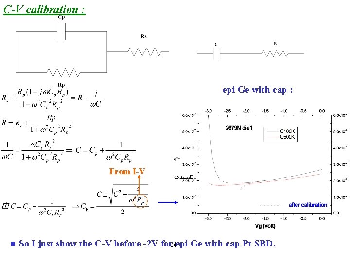
C-V calibration : epi Ge with cap : From I-V n So I just show the C-V before -2 V for 14 epi Ge with cap Pt SBD.
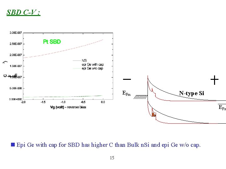
SBD C-V : EFm N-type Si EFn n Epi Ge with cap for SBD has higher C than Bulk n. Si and epi Ge w/o cap. 15
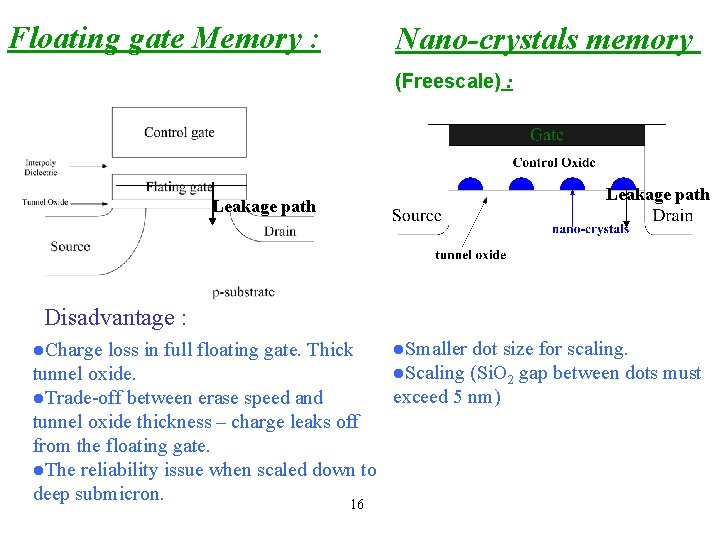
Floating gate Memory : Nano-crystals memory (Freescale) : Leakage path Disadvantage : l. Smaller dot size for scaling. loss in full floating gate. Thick l. Scaling (Si. O 2 gap between dots must tunnel oxide. exceed 5 nm) l. Trade-off between erase speed and tunnel oxide thickness – charge leaks off from the floating gate. l. The reliability issue when scaled down to deep submicron. 16 l. Charge
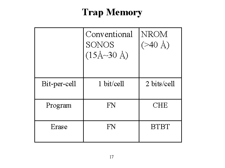
Trap Memory Conventional NROM (>40 Å) SONOS (15Å~30 Å) Bit-per-cell 1 bit/cell 2 bits/cell Program FN CHE Erase FN BTBT 17
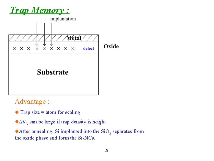
Trap Memory : Advantage : l Trap size = atom for scaling l∆VT can be large if trap density is height l. After annealing, Si implanted into the Si. O 2 separates from the oxide phase and form the Si-NCs. 18
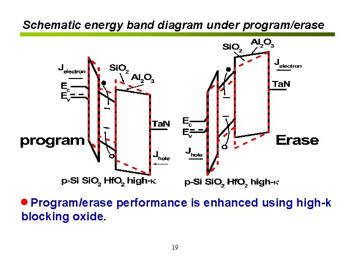
Schematic energy band diagram under program/erase Program/erase performance is enhanced using high-k blocking oxide. 19
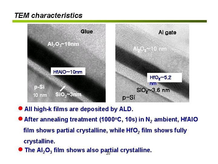
TEM characteristics Glue Al 2 O 3~10 nm Al gate Al 2 O 3~10 nm Hf. Al. O~10 nm Hf. O 2~5. 2 nm p-Si 10 nm Si. O 2~3. 6 nm p-Si All high-k films are deposited by ALD. After annealing treatment (1000 o. C, 10 s) in N 2 ambient, Hf. Al. O film shows partial crystalline, while Hf. O 2 film shows fully crystalline. The Al O film shows also partial crystalline. 2 3 20
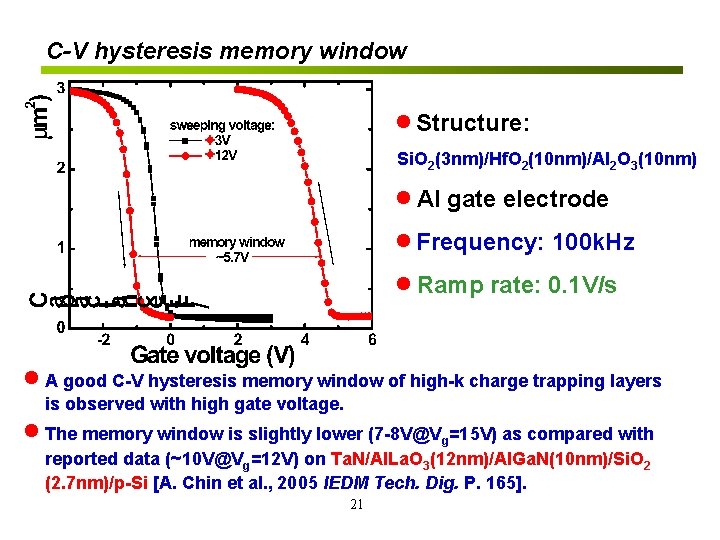
C-V hysteresis memory window Structure: Si. O 2(3 nm)/Hf. O 2(10 nm)/Al 2 O 3(10 nm) Al gate electrode Frequency: 100 k. Hz Ramp rate: 0. 1 V/s A good C-V hysteresis memory window of high-k charge trapping layers is observed with high gate voltage. The memory window is slightly lower (7 -8 V@Vg=15 V) as compared with reported data (~10 V@Vg=12 V) on Ta. N/Al. La. O 3(12 nm)/Al. Ga. N(10 nm)/Si. O 2 (2. 7 nm)/p-Si [A. Chin et al. , 2005 IEDM Tech. Dig. P. 165]. 21
- Slides: 21