b 1011 Processor to Processor ENGR x D

b 1011 Processor to Processor ENGR x. D 52 Eric Van. Wyk Fall 2014

Today • Allow our Processors out into the wild! • This is an experimental lecture • Time for HW 4 at End

… but first EMAIL ALL OF US NOT JUST LYRA IT MAKES LYRA SAD IT MAKES YOU SLOW

Check In • We’ve glanced at the full stack – Gates -> Sub-systems -> Processor -> Code • How do we talk to the rest of the world? • Example: Analog to Digital Converter

LTC 1605

LTC 1605

Timing Diagram

Timing Diagram • Conversion begins when R/C goes low – Busy is asserted – Data becomes INVALID

Timing Diagram • Conversion Finishes – Data becomes valid – Wait a moment – Busy is de-asserted

Timing Diagram • Invalid Data – Recall lecture 2: Timing and Latches • Hi-Z – Nothing asserted, line floats.
 1. Master Requests Data 2. Slave responds with data within")
Generic Parallel Access (Fast) 1. Master Requests Data 2. Slave responds with data within Access Time 3. Master reads Data, finishes Request 4. Slave ready for next request
 1. Master Requests Data 2. Slave is too slow to")
Generic Parallel Access (Slow) 1. Master Requests Data 2. Slave is too slow to respond within Access Time, Asserts WAIT 3. Slave deasserts wait after providing data 4. Master receives, stops request 5. Slave ready for next request

Parallel Port • N Data Pins • Control Pins: – Request Behaviors – Indicate Readiness • What if we need more Data? – Add More Pins

Pseudo Parallel Port • D Flip Flops to re-use existing Data Pins • Total Controlled Bits: – D Data Pins – L Latch Pins – DL Total

Pseudo Parallel Port

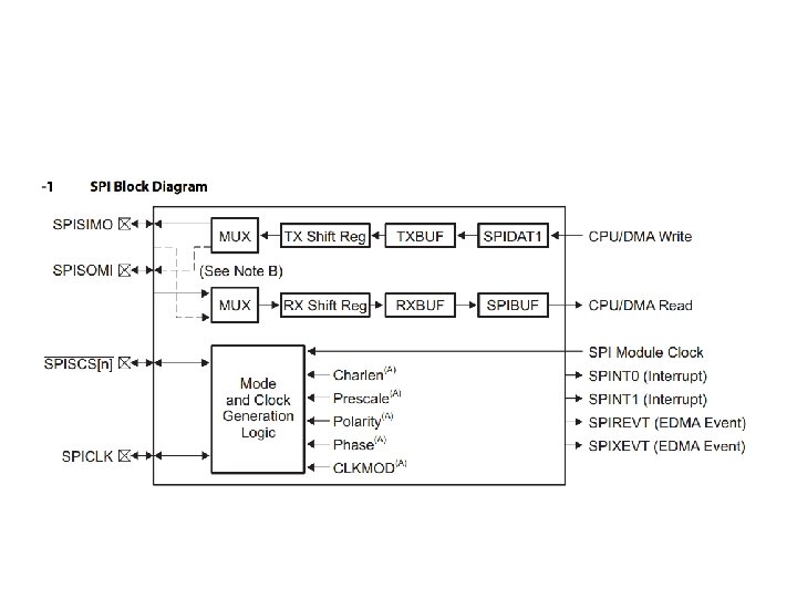
Serial Peripheral Interface • One data pin per direction – MOSI – Master Out Slave In – MISO – Master In Slave Out • One Clock Pin – Replaces all of the Latch Pins • Chip Select – Tells a peripheral we’re talking to it • One bit of data per clock strobe

Multiple Peripherals require individual Chip Select

Implementation • Basically, Shift Registers

UART • Universal Asynchronous Receiver Transmitter • One Data Pin per Direction – Inconsistently Named – Rx? Tx? • No Clock Pin!

UART Clocking • No Explicit Clock • Instead, agree on speed and hope for the best

UART Clocking • Starts High • Drops low to start – Start Bit • Data Bits are sent • Remains High to recover – Stop Bit(s) • Receiver measures data halfway through each bit – In case of clock error 1. 5 Bit Times

UART Clock Error • “Correct” Sampling Time Drifted Sampling Time

Serial Vs Parallel Serial • One Word at a time • Cheaper Logic • One Bit at a time • Cheaper Wiring • Fast for short distances • Fast for long distances – Many bits per clock – Faster Clock possible • Distance affects maximum clock rate: – Capacitance affects slew time • Slowly charge wire, delays stability – Wire length mismatch creates skew time • Some signals arrive sooner than others – Parallel wires create extra capacitance • Parallel is more affected than Serial

Bi-Directionality • So far, every pin has a defined direction – This can be done with normal gates! • To do bidirectional, we need new equipment

Lets get PHYsical • PHY interfaces logic with the physical world • Needed whenever we go “off chip” • Simplest PHY is an inverter. – Orientation determines input vs output

GPIO • Input is a Buffer – Cleans signal for internal logic • Output Tri-State Buffer – Can “release” the line – Only asserts when enabled

Tri. State Buffer • When Enable is true, acts like a normal buffer – PFET on for Input = 1 – NFET on for Input = 0 • When Enable is false, doesn’t assert a state – Neither FET is on – Output “Floats” – Output = Z or Hi-Z http: //www-mdp. eng. cam. ac. uk/web/library/enginfo/mdp_micro/lecture 1 -5 -4. html

PSOC GPIO Structure http: //www. cypress. com/

http: //www. ti. com/lit/ug/sprueq 8 a. pdf

I 2 C = Inter-Integrated Circuit • Two Wire Serial Protocol – SDA = Serial DAta – SCL = Serial Clock • 7 bit addressing: Up to 127 devices per bus – … unless capacitance kills you (400 p. F nom max)

Whose Line is it, Anyway? • No Chip Select Lines • Each message has an address preamble – If it isn’t for you, ignore it.

Bidirectionality • Lines have Pullup Resistors – Gently pulls it to VDD – Default state is 1 • Devices yank to ground to assert a zero – If no one asserts 0, it is a 1 – This is called “Open Drain”

I 2 C Bus Transfer Multiple bytes sent in a transaction; every 8 bits has a 9 th bit that is an acknowledge. V 0. 3 33

I 2 C • Pull-Ups limit max clock frequency – VERY sensitive to total capacitance • 400 p. F max – Slower than other serial protocols • 100 k. Hz Normal, 400 k. Hz Enhanced – Higher R, Slower max frequency – Lower R, Higher power dissipation • Addresses can be a pain! – Not all bits are definable – Overlap happens more often than you’d expect!

CAN – Controller Area Network • Typically found in Vehicles, Robots • 1 Megabit per Second, 11 bit addressing • Dominant / Recessive Signalling • No Separate Clock Signal

CAN - Dominance • Like I 2 C, Dominant vs Recessive – Requires a separate PHY chip • To Assert: – Pull CAN HI up – Pull CAN LO down – Otherwise, resistor pulls two wires back

CAN - Frame • Green – Address • Yellow – Data Length in Bytes • Red – Actual Data

TL; DR; • Data Width – Parallel – Serial • Timing: • Targets – One to One – Broadcast with Address – Broadcast with Select – Explicit / Shared Clock • PHY – Assumed Clock – GPIO? – Clock Recovery – Explicit PHY – Asynchronous (Ick)

Memory Mapped Peripherals • Pretend that Peripherals are weird Memory • Registers that control peripherals are write-only memory addresses • Registers that receive data are read-only • Following Slides are derived from http: //www. ti. com/lit/ug/sprugp 2 a. pdf

HW 4 • Behavioral • First 6 Deliverables should take <2 Hour Total – Unless you are doing them wrong

Registers • Deliverable 1 – Use DFF as a component – Don’t draw its implementation • Deliverable 2 – Copy paste, add 14 characters • Deliverable 3 – Copy paste, “Assign _____ = 0”

Test Bench • Xxxx = 42? • YUP

With Remaining Time • Work On HW 4

ADC 0803 • 8 Bit Differential ADC • 135 ns Sample Time

MAX 114/MAX 118
![• DB[7: 0] – Data Bits • RD – Pull low to begin](http://slidetodoc.com/presentation_image/1dbe29728afe0136fca816629df27899/image-49.jpg "• DB[7: 0] – Data Bits • RD – Pull low to begin")
• DB[7: 0] – Data Bits • RD – Pull low to begin reading • INT – Pulled low to indicate conversion finish

Timing Diagram

Instruction Mapped Peripheral
- Slides: 51