AVS 2002 Nov 3 Nov 8 2002 Denver
- Slides: 23

AVS 2002 Nov 3 - Nov 8, 2002 Denver, Colorado INTEGRATED MODELING OF ETCHING, CLEANING AND BARRIER COATING PVD FOR POROUS AND CONVENTIONAL SIO 2 IN FLUOROCARBON BASED CHEMISTRIES* Arvind Sankaran 1 and Mark J. Kushner 2 1 Department of Chemical Engineering 2 Department of Electrical and Computer Engineering University of Illinois, Urbana, IL 61801, USA email: asankara@uiuc. edu mjk@uiuc. edu http: //uigelz. ece. uiuc. edu AVS 99 - *Work supported by SRC, NSF and SEMATECH

AGENDA · Low dielectric constant materials · Surface reaction mechanism and validation · Fluorocarbon etching of Si. O 2/Si · Ar/O 2 etching of organic polymer · High aspect ratio etching of porous and non porous Si. O 2 · Integrated Modeling: Ar/O 2 strip of polymer and IMPVD · Concluding Remarks AVS 03_AS_02 University of Illinois Optical and Discharge Physics

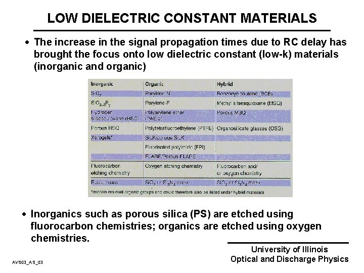
LOW DIELECTRIC CONSTANT MATERIALS · The increase in the signal propagation times due to RC delay has brought the focus onto low dielectric constant (low-k) materials (inorganic and organic) · Inorganics such as porous silica (PS) are etched using fluorocarbon chemistries; organics are etched using oxygen chemistries. AVS 03_AS_03 University of Illinois Optical and Discharge Physics

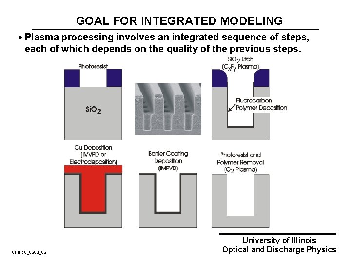
GOAL FOR INTEGRATED MODELING · Plasma processing involves an integrated sequence of steps, each of which depends on the quality of the previous steps. CFDRC_0503_05 University of Illinois Optical and Discharge Physics

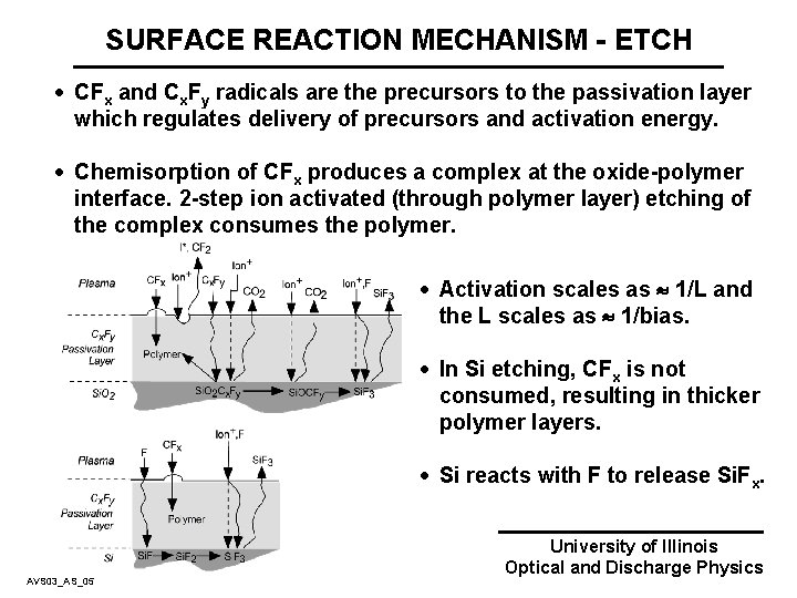
SURFACE REACTION MECHANISM - ETCH · CFx and Cx. Fy radicals are the precursors to the passivation layer which regulates delivery of precursors and activation energy. · Chemisorption of CFx produces a complex at the oxide-polymer interface. 2 -step ion activated (through polymer layer) etching of the complex consumes the polymer. · Activation scales as 1/L and the L scales as 1/bias. · In Si etching, CFx is not consumed, resulting in thicker polymer layers. · Si reacts with F to release Si. Fx. AVS 03_AS_05 University of Illinois Optical and Discharge Physics

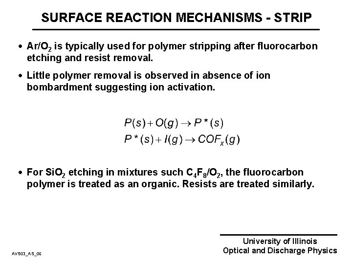
SURFACE REACTION MECHANISMS - STRIP · Ar/O 2 is typically used for polymer stripping after fluorocarbon etching and resist removal. · Little polymer removal is observed in absence of ion bombardment suggesting ion activation. · For Si. O 2 etching in mixtures such C 4 F 8/O 2, the fluorocarbon polymer is treated as an organic. Resists are treated similarly. AVS 03_AS_06 University of Illinois Optical and Discharge Physics

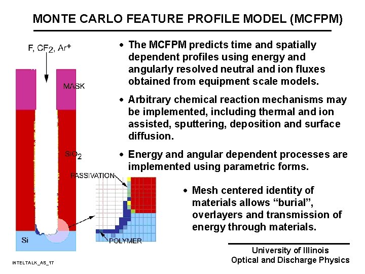
MONTE CARLO FEATURE PROFILE MODEL (MCFPM) · The MCFPM predicts time and spatially dependent profiles using energy and angularly resolved neutral and ion fluxes obtained from equipment scale models. · Arbitrary chemical reaction mechanisms may be implemented, including thermal and ion assisted, sputtering, deposition and surface diffusion. · Energy and angular dependent processes are implemented using parametric forms. · Mesh centered identity of materials allows “burial”, overlayers and transmission of energy through materials. INTELTALK_AS_17 University of Illinois Optical and Discharge Physics

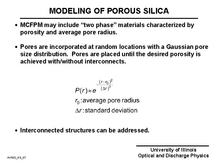
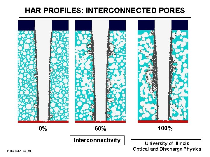
MODELING OF POROUS SILICA · MCFPM may include “two phase” materials characterized by porosity and average pore radius. · Pores are incorporated at random locations with a Gaussian pore size distribution. Pores are placed until the desired porosity is achieved with/without interconnects. · Interconnected structures can be addressed. AVS 03_AS_07 University of Illinois Optical and Discharge Physics

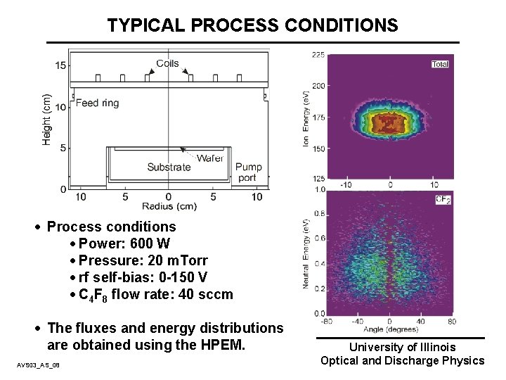
TYPICAL PROCESS CONDITIONS · Process conditions · Power: 600 W · Pressure: 20 m. Torr · rf self-bias: 0 -150 V · C 4 F 8 flow rate: 40 sccm · The fluxes and energy distributions are obtained using the HPEM. AVS 03_AS_08 University of Illinois Optical and Discharge Physics

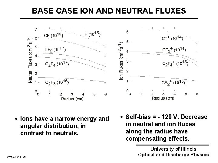
BASE CASE ION AND NEUTRAL FLUXES · Ions have a narrow energy and angular distribution, in contrast to neutrals. AVS 03_AS_09 · Self-bias = - 120 V. Decrease in neutral and ion fluxes along the radius have compensating effects. University of Illinois Optical and Discharge Physics

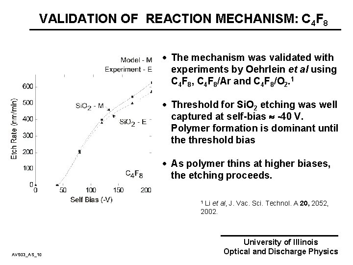
VALIDATION OF REACTION MECHANISM: C 4 F 8 · The mechanism was validated with experiments by Oehrlein et al using C 4 F 8, C 4 F 8/Ar and C 4 F 8/O 2. 1 · Threshold for Si. O 2 etching was well captured at self-bias -40 V. Polymer formation is dominant until the threshold bias · As polymer thins at higher biases, the etching proceeds. 1 Li et al, J. Vac. Sci. Technol. A 20, 2052, 2002. AVS 03_AS_10 University of Illinois Optical and Discharge Physics

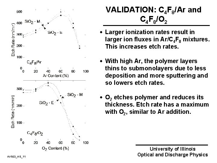
VALIDATION: C 4 F 8/Ar and C 4 F 8/O 2 · Larger ionization rates result in larger ion fluxes in Ar/C 4 F 8 mixtures. This increases etch rates. · With high Ar, the polymer layers thins to submonolayers due to less deposition and more sputtering and so lowers etch rates. · O 2 etches polymer and reduces its thickness. Etch rate has a maximum with O 2, similar to Ar addition. AVS 03_AS_11 University of Illinois Optical and Discharge Physics

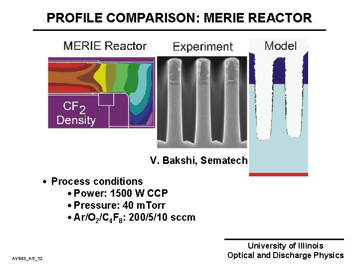
PROFILE COMPARISON: MERIE REACTOR V. Bakshi, Sematech · Process conditions · Power: 1500 W CCP · Pressure: 40 m. Torr · Ar/O 2/C 4 F 8: 200/5/10 sccm AVS 03_AS_12 University of Illinois Optical and Discharge Physics

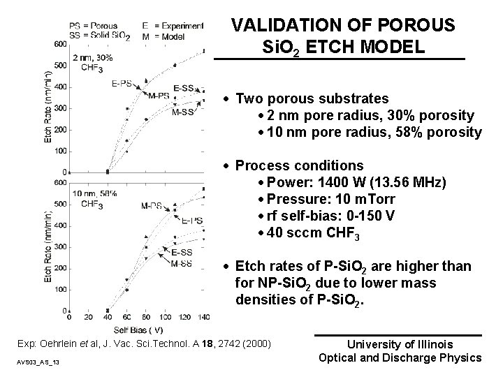
VALIDATION OF POROUS Si. O 2 ETCH MODEL · Two porous substrates · 2 nm pore radius, 30% porosity · 10 nm pore radius, 58% porosity · Process conditions · Power: 1400 W (13. 56 MHz) · Pressure: 10 m. Torr · rf self-bias: 0 -150 V · 40 sccm CHF 3 · Etch rates of P-Si. O 2 are higher than for NP-Si. O 2 due to lower mass densities of P-Si. O 2. Exp: Oehrlein et al, J. Vac. Sci. Technol. A 18, 2742 (2000) AVS 03_AS_13 University of Illinois Optical and Discharge Physics

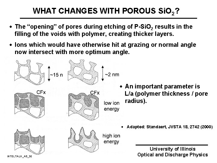
WHAT CHANGES WITH POROUS Si. O 2? · The “opening” of pores during etching of P-Si. O 2 results in the filling of the voids with polymer, creating thicker layers. · Ions which would have otherwise hit at grazing or normal angle now intersect with more optimum angle. · An important parameter is L/a (polymer thickness / pore radius). · Adapted: Standaert, JVSTA 18, 2742 (2000) INTELTALK_AS_30 University of Illinois Optical and Discharge Physics

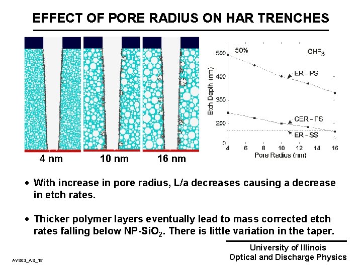
EFFECT OF PORE RADIUS ON HAR TRENCHES 4 nm 10 nm 16 nm · With increase in pore radius, L/a decreases causing a decrease in etch rates. · Thicker polymer layers eventually lead to mass corrected etch rates falling below NP-Si. O 2. There is little variation in the taper. AVS 03_AS_15 University of Illinois Optical and Discharge Physics

HAR PROFILES: INTERCONNECTED PORES 0% 60% Interconnectivity INTELTALK_AS_40 100% University of Illinois Optical and Discharge Physics

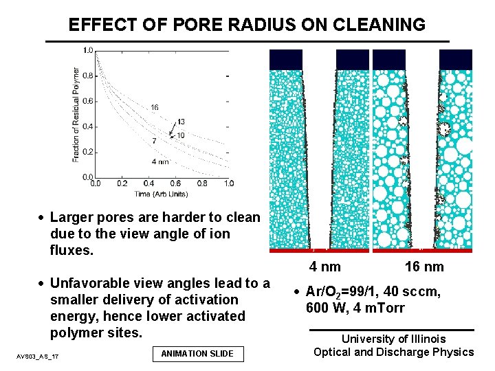
EFFECT OF PORE RADIUS ON CLEANING · Larger pores are harder to clean due to the view angle of ion fluxes. · Unfavorable view angles lead to a smaller delivery of activation energy, hence lower activated polymer sites. AVS 03_AS_17 ANIMATION SLIDE 4 nm 16 nm · Ar/O 2=99/1, 40 sccm, 600 W, 4 m. Torr University of Illinois Optical and Discharge Physics

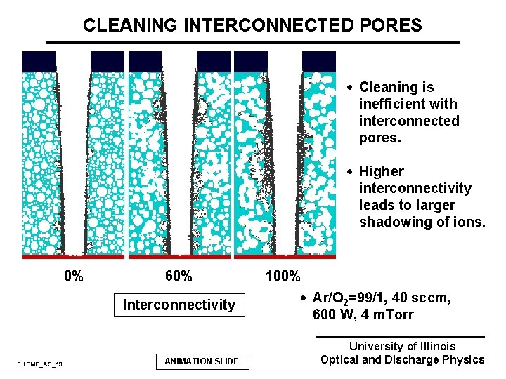
CLEANING INTERCONNECTED PORES · Cleaning is inefficient with interconnected pores. · Higher interconnectivity leads to larger shadowing of ions. 0% 60% Interconnectivity CHEME_AS_19 ANIMATION SLIDE 100% · Ar/O 2=99/1, 40 sccm, 600 W, 4 m. Torr University of Illinois Optical and Discharge Physics

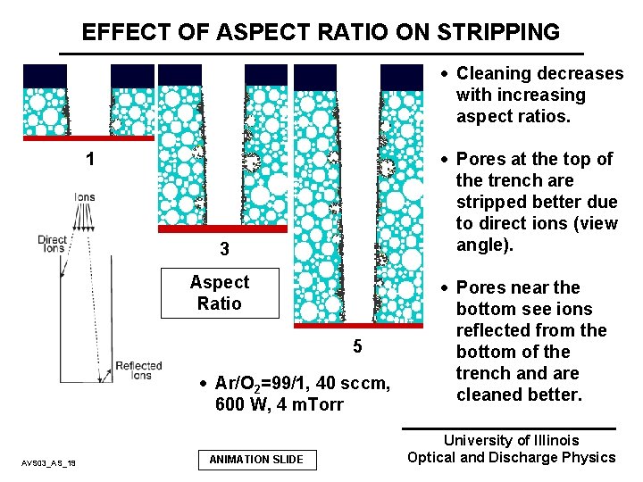
EFFECT OF ASPECT RATIO ON STRIPPING · Cleaning decreases with increasing aspect ratios. · Pores at the top of the trench are stripped better due to direct ions (view angle). 1 3 Aspect Ratio 5 · Ar/O 2=99/1, 40 sccm, 600 W, 4 m. Torr AVS 03_AS_19 ANIMATION SLIDE · Pores near the bottom see ions reflected from the bottom of the trench and are cleaned better. University of Illinois Optical and Discharge Physics

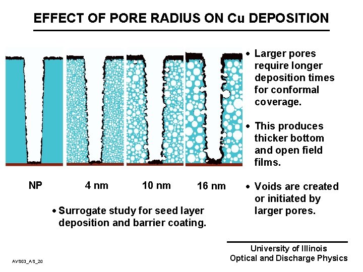
EFFECT OF PORE RADIUS ON Cu DEPOSITION · Larger pores require longer deposition times for conformal coverage. · This produces thicker bottom and open field films. NP 4 nm 10 nm 16 nm · Surrogate study for seed layer deposition and barrier coating. AVS 03_AS_20 · Voids are created or initiated by larger pores. University of Illinois Optical and Discharge Physics

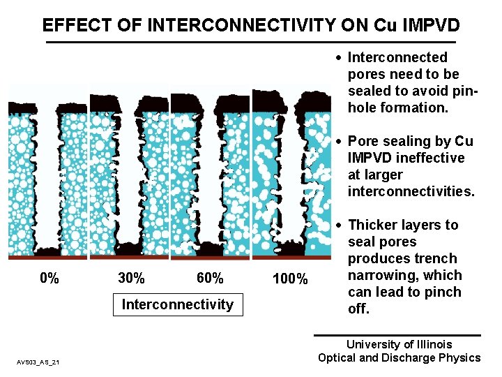
EFFECT OF INTERCONNECTIVITY ON Cu IMPVD · Interconnected pores need to be sealed to avoid pinhole formation. · Pore sealing by Cu IMPVD ineffective at larger interconnectivities. 0% 30% 60% Interconnectivity AVS 03_AS_21 100% · Thicker layers to seal pores produces trench narrowing, which can lead to pinch off. University of Illinois Optical and Discharge Physics

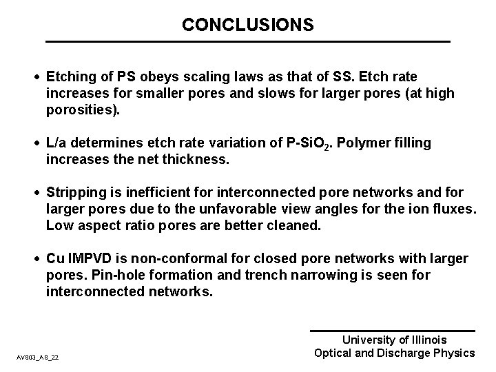
CONCLUSIONS · Etching of PS obeys scaling laws as that of SS. Etch rate increases for smaller pores and slows for larger pores (at high porosities). · L/a determines etch rate variation of P-Si. O 2. Polymer filling increases the net thickness. · Stripping is inefficient for interconnected pore networks and for larger pores due to the unfavorable view angles for the ion fluxes. Low aspect ratio pores are better cleaned. · Cu IMPVD is non-conformal for closed pore networks with larger pores. Pin-hole formation and trench narrowing is seen for interconnected networks. AVS 03_AS_22 University of Illinois Optical and Discharge Physics