
AVR Chapter 1 Embedded System address memory 200
AVR - Chapter 1 황지연
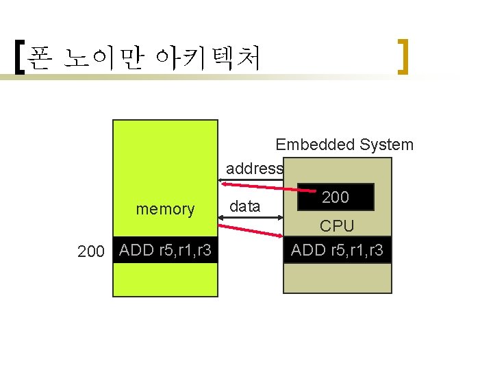
폰 노이만 아키텍처 Embedded System address memory 200 ADD r 5, r 1, r 3 data 200 CPU ADD IR r 5, r 1, r 3
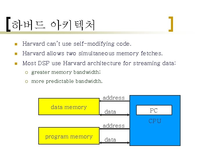
하버드 아키텍처 n Harvard can’t use self-modifying code. n Harvard allows two simultaneous memory fetches. n Most DSP use Harvard architecture for streaming data: ¡ greater memory bandwidth; ¡ more predictable bandwidth. address data memory data address program memory data PC CPU
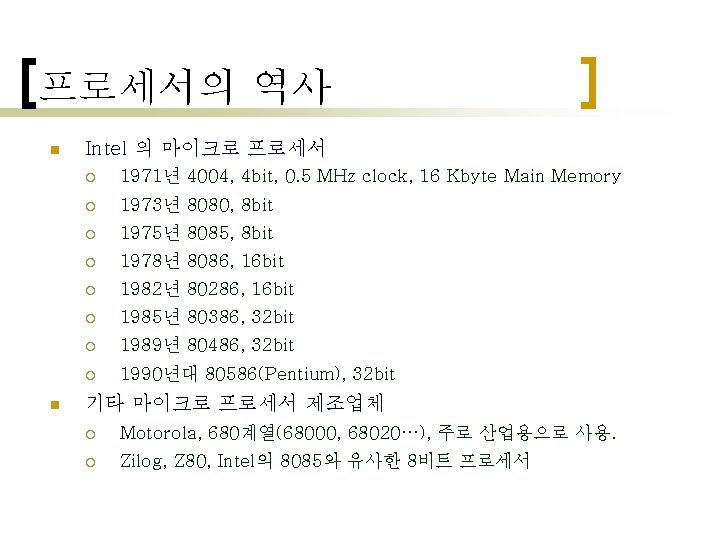
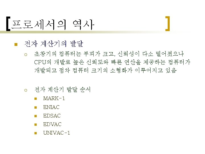
프로세서의 역사 n n Intel 의 마이크로 프로세서 ¡ 1971년 4004, 4 bit, 0. 5 MHz clock, 16 Kbyte Main Memory ¡ 1973년 8080, 8 bit ¡ 1975년 8085, 8 bit ¡ 1978년 8086, 16 bit ¡ 1982년 80286, 16 bit ¡ 1985년 80386, 32 bit ¡ 1989년 80486, 32 bit ¡ 1990년대 80586(Pentium), 32 bit 기타 마이크로 프로세서 제조업체 ¡ Motorola, 680계열(68000, 68020…), 주로 산업용으로 사용. ¡ Zilog, Z 80, Intel의 8085와 유사한 8비트 프로세서
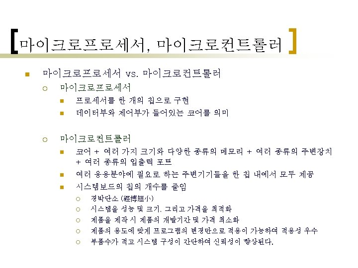
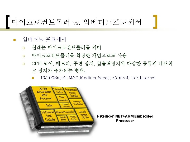
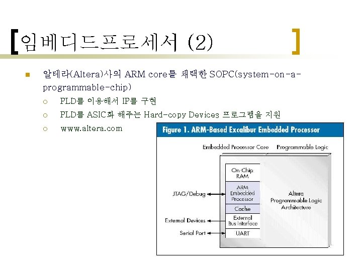
임베디드프로세서 (2) n 알테라(Altera)사의 ARM core를 채택한 SOPC(system-on-aprogrammable-chip) ¡ PLD를 이용해서 IP를 구현 ¡ PLD를 ASIC화 해주는 Hard-copy Devices 프로그램을 지원 ¡ www. altera. com
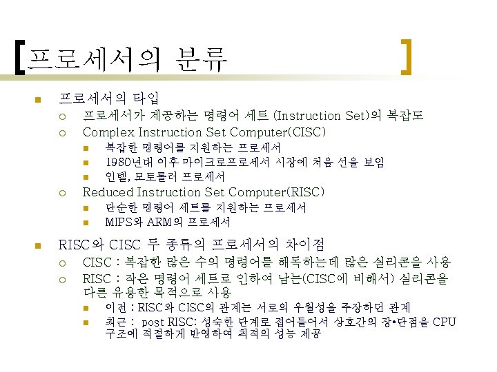
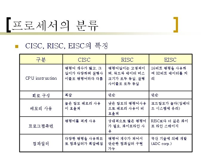
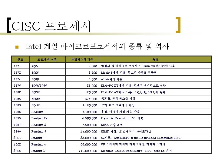
CISC 프로세서 n 연도 Intel 계열 마이크로프로세서의 종류 및 역사 프로세서 이름 트렌지스터 개수 특징 1971 4004 2, 250 인텔의 첫 마이크로 프로세스, Busicom 계산기에 사용 1972 8008 2, 500 Mark-8에서 사용, 최초의 가정용 컴퓨터 1974 8080 5, 000 Altair에서 사용 1978 8086/8088 1982 29, 000 IBM-PC XT에서 사용, 인텔이 대기업으로 성장 80286 120, 000 IBM-PC AT에서 사용, 6년간 천 5백만대 판매 1985 80386 275, 000 32비트 멀티 테스킹 지원 1989 80486 1, 180, 000 수치 보조 프로세서 내장 1993 Pentium 3, 100, 000 음성, 이미지 처리 기능 강화 1995 Pentium Pro 5, 500, 000 Dynamic Execution 구조 채택 1997 Pentium 2 7, 500, 000 MMX 기술 지원 1999 Pentium 3 24, 000 SIMD 지원, 12 스테이지 파이프라인 2001 Itanium 25, 000 64비트, Explicitly Parallel Instruction Computing(EPIC) 2002 Pentium 4 55, 000 20 스테이지 하이퍼 파이프라인, 하이퍼 쓰레딩 2003 Itanium 2 410, 000 Machine Check Architecture, EPIC, 6 MB L 3 캐시
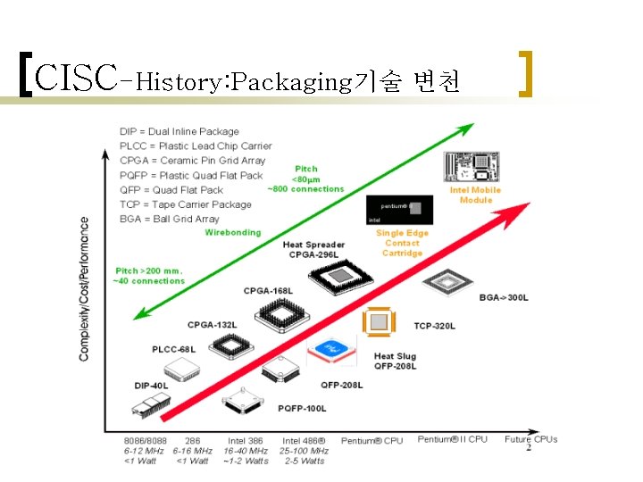
CISC-History: Packaging기술 변천
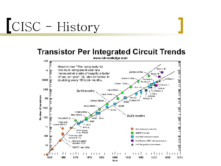
CISC - History
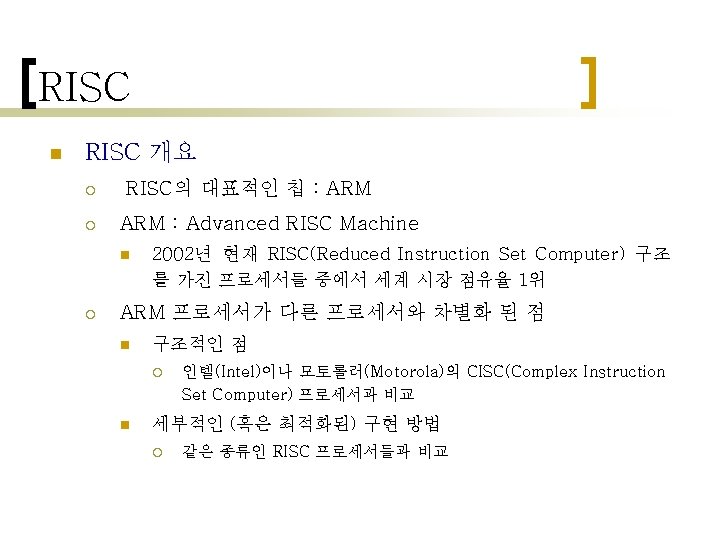
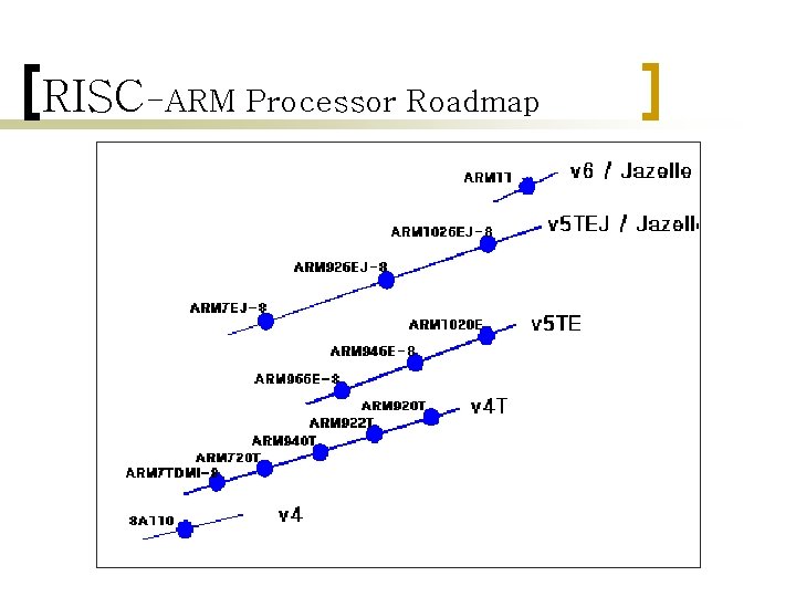
RISC-ARM Processor Roadmap
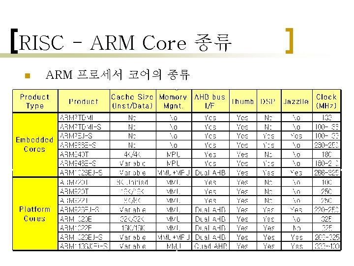
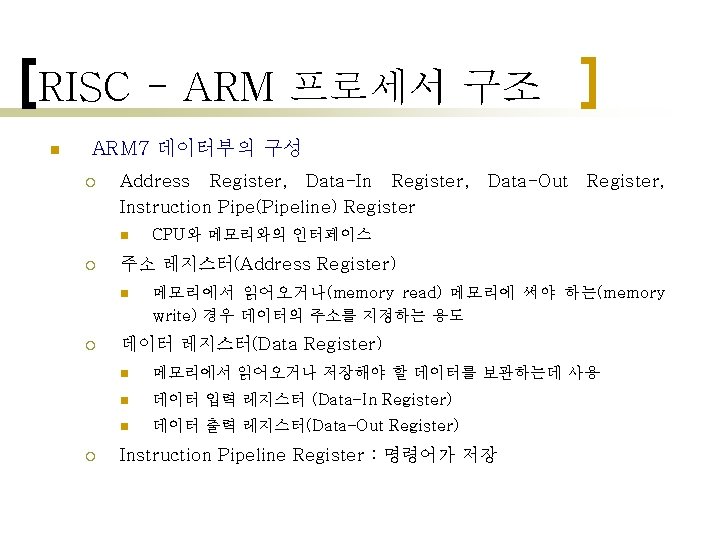

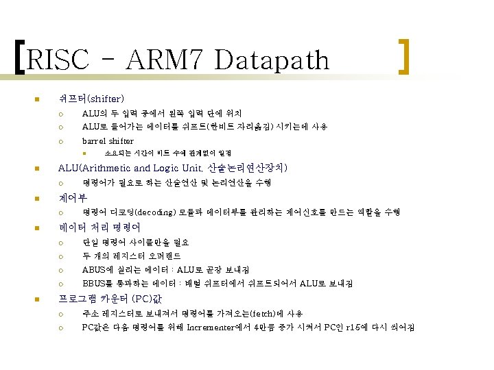
RISC - ARM 7 블록도
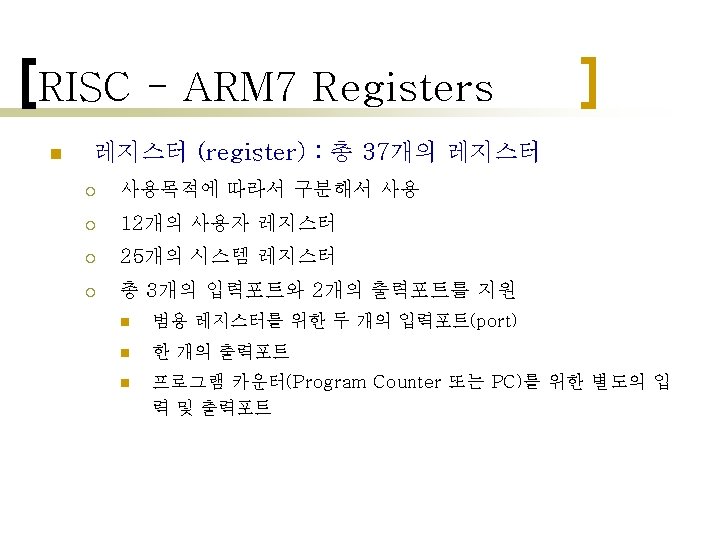
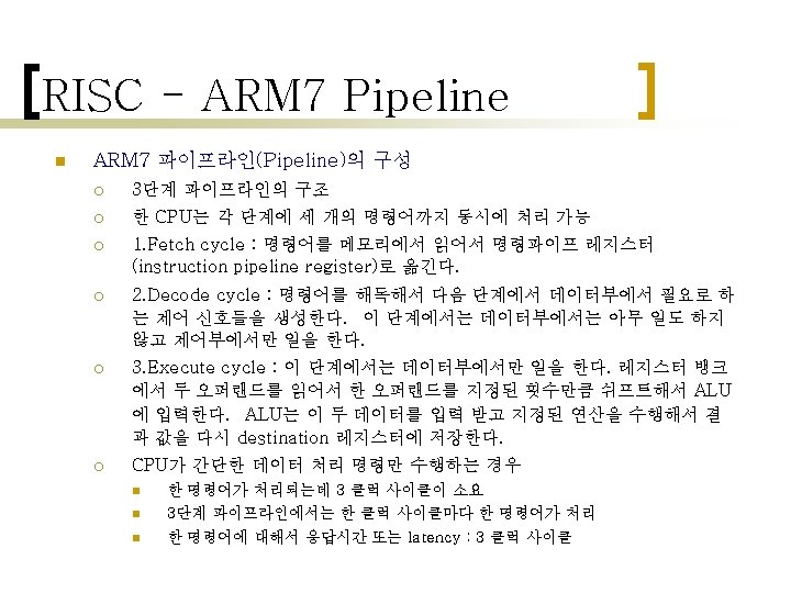
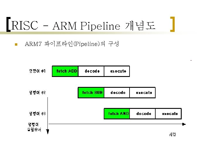
RISC - ARM Pipeline 개념도 n ARM 7 파이프라인(Pipeline)의 구성
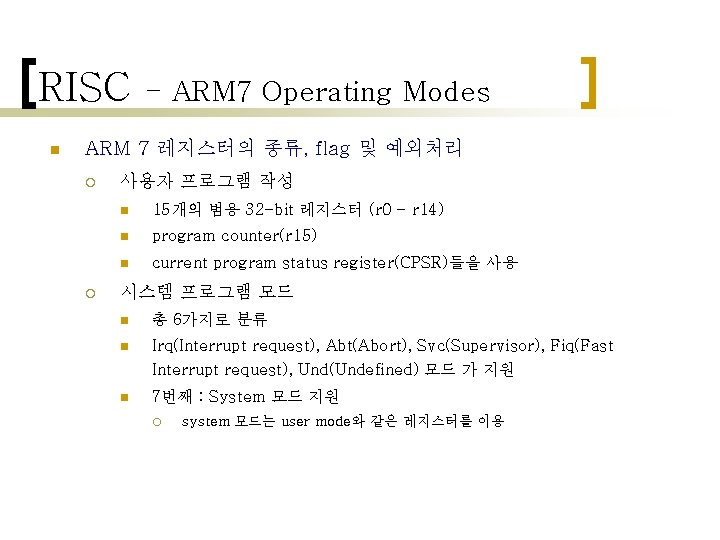
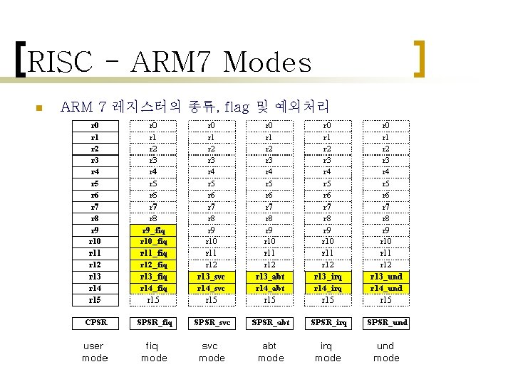
RISC n - ARM 7 Operating Modes ARM 7 레지스터의 종류, flag 및 예외처리 ¡ ¡ 사용자 프로그램 작성 n 15개의 범용 32 -bit 레지스터 (r 0 - r 14) n program counter(r 15) n current program status register(CPSR)들을 사용 시스템 프로그램 모드 n 총 6가지로 분류 n Irq(Interrupt request), Abt(Abort), Svc(Supervisor), Fiq(Fast Interrupt request), Und(Undefined) 모드 가 지원 n 7번째 : System 모드 지원 ¡ system 모드는 user mode와 같은 레지스터를 이용
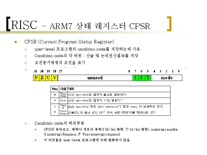
RISC n - ARM 7 상태 레지스터 CPSR (Current Program Status Register) ¡ user-level 프로그램의 condition code를 저장하는데 사용 ¡ Condition code의 각 비트 : 산술 및 논리연산결과를 저장 ¡ 조건분기명령의 조건을 표시 ¡ condition code의 구성 ¡ Condition code의 하위부분 n CPU의 동작모드, 명령어 세트의 종류(I: 32 -bit 명령, T: 16 -bit 명령), interrupt enable (I: interrupt Request, F: Fast interrupt request) n 이 비트들은 user-level 프로그램에 의해 변화하지 않음
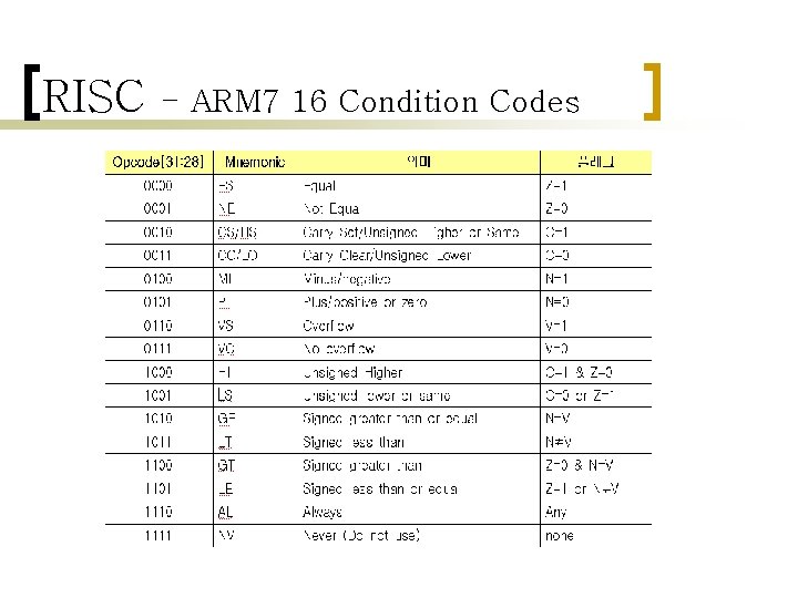
RISC - ARM 7 16 Condition Codes
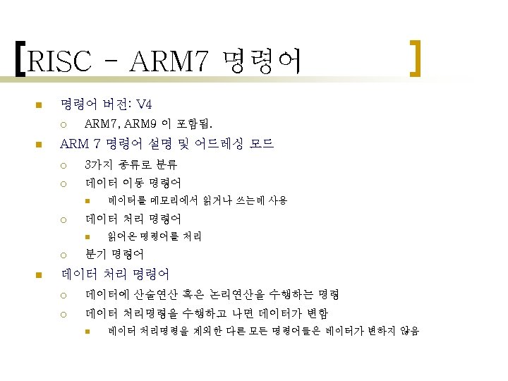
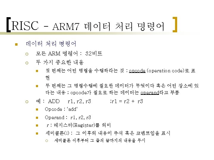
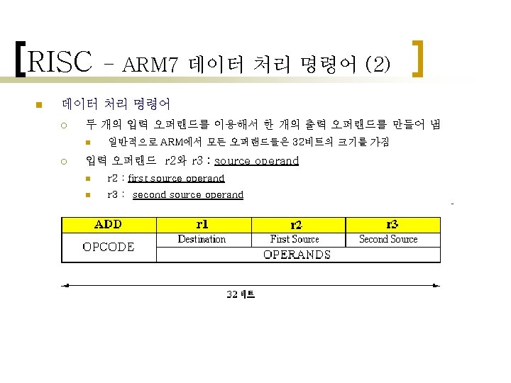
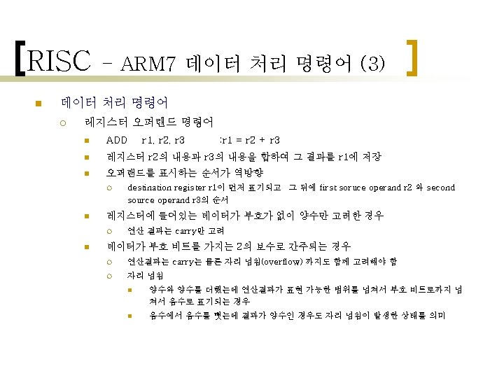
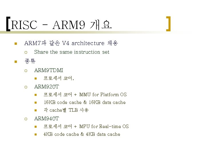
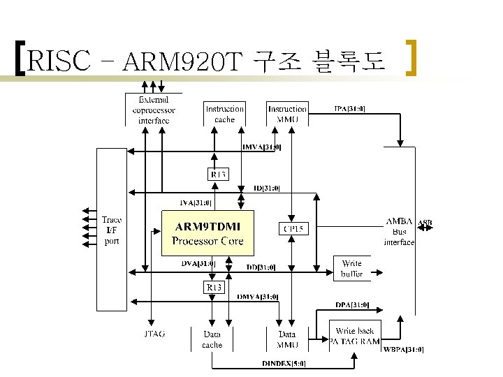
RISC - ARM 9 개요 n ARM 7과 같은 V 4 architecture 채용 ¡ n Share the same instruction set 종류 ¡ ARM 9 TDMI n ¡ ¡ 프로세서 코어, ARM 920 T n 프로세서 코어 + MMU for Platform OS n 16 KB code cache & 16 KB data cache n 각 cache별 TLB 사용 ARM 940 T n 프로세서 코어 + MPU for Real-time OS n 4 KB code cache & 4 KB data cache
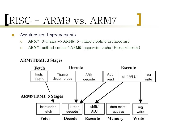
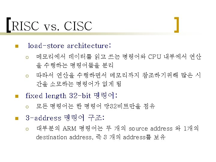
RISC - ARM 9 vs. ARM 7 n Architecture Improvements ¡ ARM 7: 3 -stage => ARM 9: 5 -stage pipeline architecture ¡ ARM 7: unified cache=>ARM 9: separate cache (Harvard arch. )
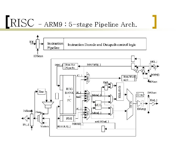
RISC - ARM 9 : 5 -stage Pipeline Arch.
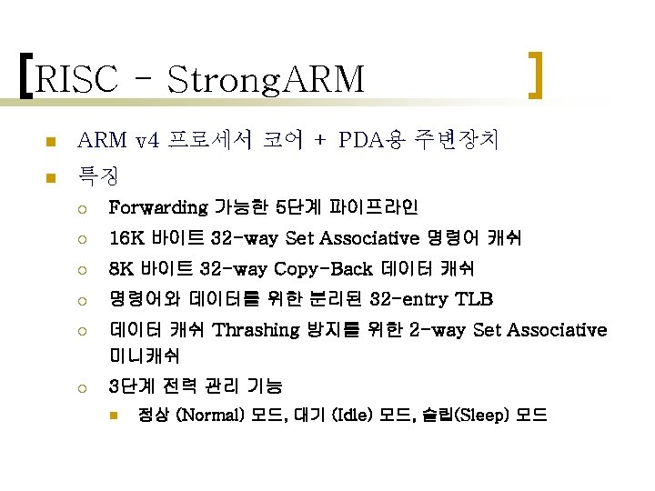
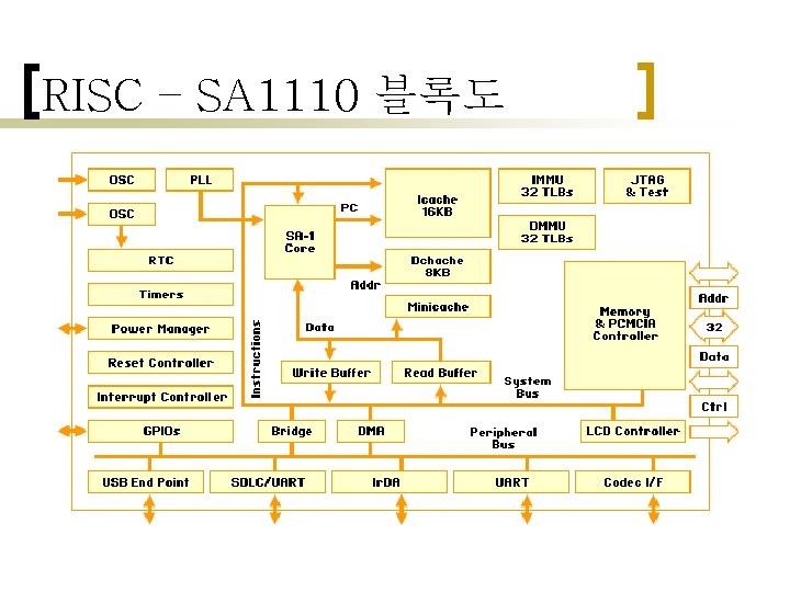
RISC – SA 1110 블록도
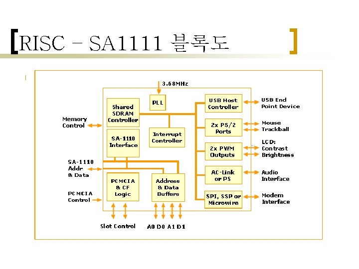
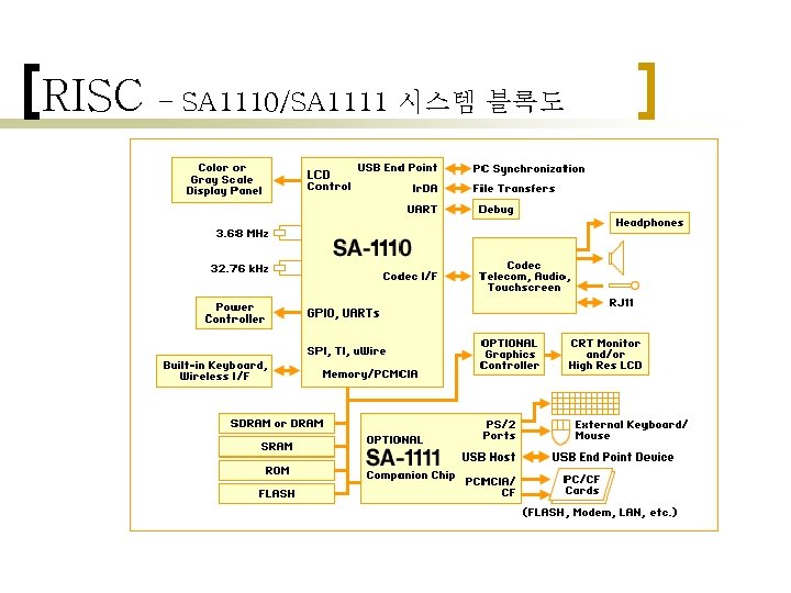
RISC – SA 1110/SA 1111 시스템 블록도
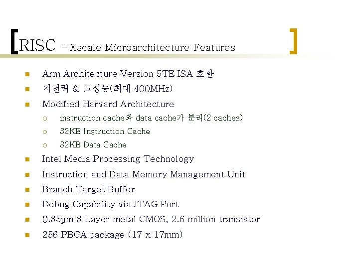
RISC – Xscale Microarchitecture Features n Arm Architecture Version 5 TE ISA 호환 n 저전력 & 고성능(최대 400 MHz) n Modified Harvard Architecture ¡ instruction cache와 data cache가 분리(2 caches) ¡ 32 KB Instruction Cache ¡ 32 KB Data Cache n Intel Media Processing Technology n Instruction and Data Memory Management Unit n Branch Target Buffer n Debug Capability via JTAG Port n 0. 35μm 3 Layer metal CMOS, 2. 6 million transistor n 256 PBGA package (17 x 17 mm)
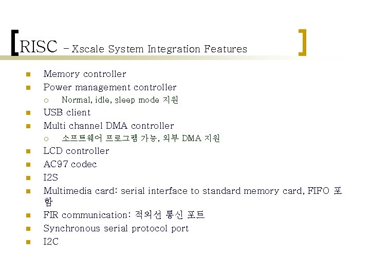
RISC n n Memory controller Power management controller ¡ n n n n Normal, idle, sleep mode 지원 USB client Multi channel DMA controller ¡ n – Xscale System Integration Features 소프트웨어 프로그램 가능, 외부 DMA 지원 LCD controller AC 97 codec I 2 S Multimedia card: serial interface to standard memory card, FIFO 포 함 FIR communication: 적외선 통신 포트 Synchronous serial protocol port I 2 C
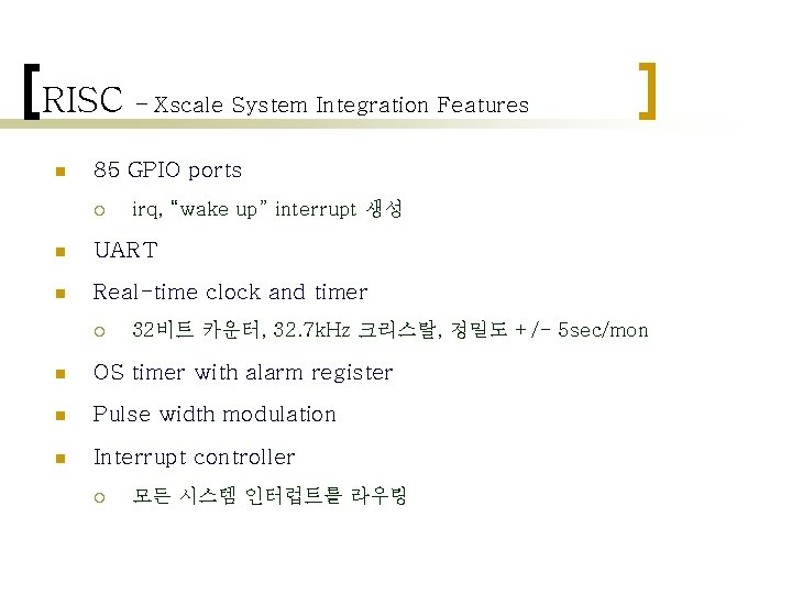
RISC n – Xscale System Integration Features 85 GPIO ports ¡ irq, “wake up” interrupt 생성 n UART n Real-time clock and timer ¡ 32비트 카운터, 32. 7 k. Hz 크리스탈, 정밀도 +/- 5 sec/mon n OS timer with alarm register n Pulse width modulation n Interrupt controller ¡ 모든 시스템 인터럽트를 라우팅
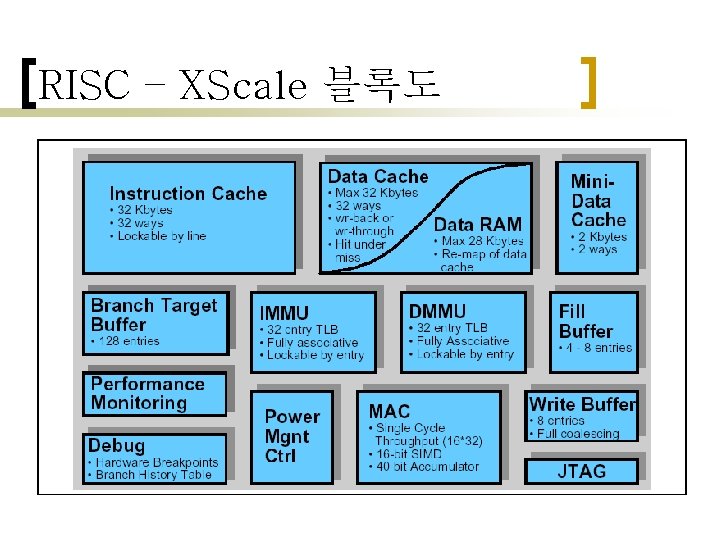
RISC – XScale 블록도 n Architecture : V 5 TE로 발전
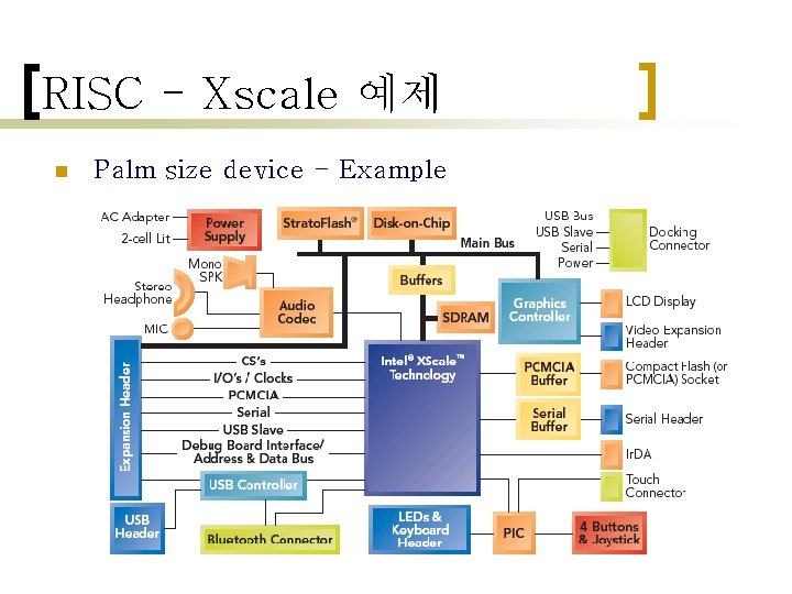
RISC - Xscale 예제 n Palm size device - Example
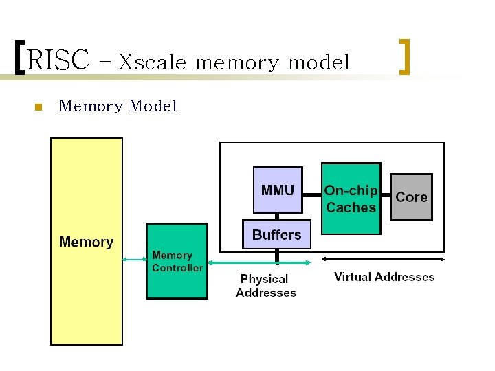
RISC n – Xscale memory model Memory Model
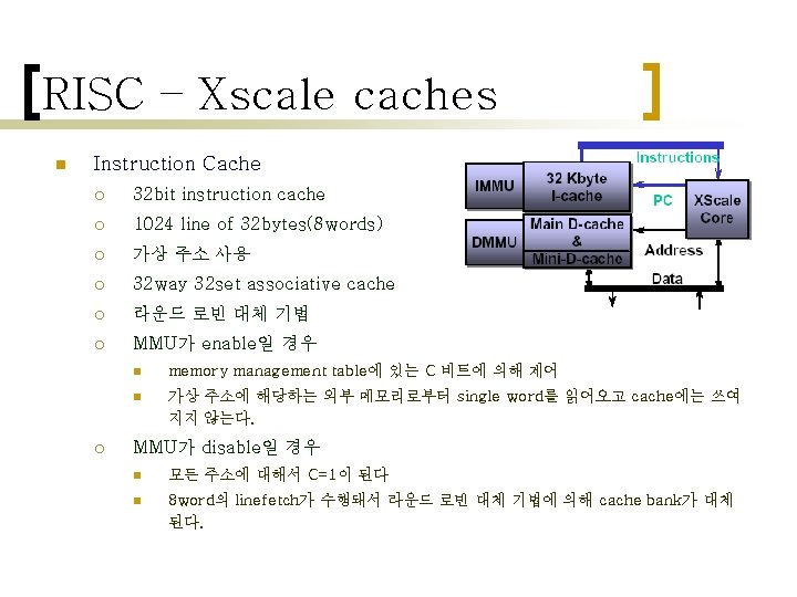
RISC – Xscale caches n Instruction Cache ¡ 32 bit instruction cache ¡ 1024 line of 32 bytes(8 words) ¡ 가상 주소 사용 ¡ 32 way 32 set associative cache ¡ 라운드 로빈 대체 기법 ¡ MMU가 enable일 경우 ¡ n memory management table에 있는 C 비트에 의해 제어 n 가상 주소에 해당하는 외부 메모리로부터 single word를 읽어오고 cache에는 쓰여 지지 않는다. MMU가 disable일 경우 n 모든 주소에 대해서 C=1이 된다 n 8 word의 linefetch가 수행돼서 라운드 로빈 대체 기법에 의해 cache bank가 대체 된다.
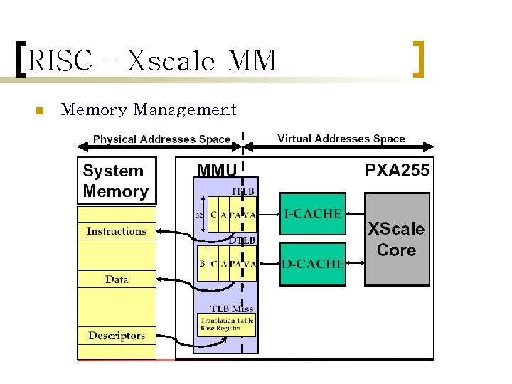
RISC – Xscale MM n Memory Management
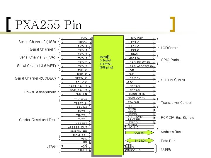
PXA 255 Pin Serial Channel 0 (USB) Serial Channel 1 Serial Channel 2 (Ir. DA) Serial Channel 3 (UART) Serial Channel 4(CODEC) Power Management Clocks, Reset and Test JTAG UDCUDC+ RXD_1 TXD_1 RXD_2 TXD_2 RXD_3 TXD_C RXD_C SFRM_C SCLK_C BATT_FAULT VDD_FAULT PWR_EN TCK_BYP TESTCLK PEXTAL PXTAL TEXTAL TXTAL n. RESET_OUT SMROM_EN ROM_SEL TCK TDI TDO TMS n. TRST Intelⓡ XScale* PXA 250 [256 -pins] L_DD(15: 0) L_FCLK L_LCLK L_PCLK L_BIAS GP(27: 0) n. CAS/ DQM(3: 0) n. RAS/ n. SDCS(3: 0) n. OE n. WE n. CS(5: 0) RDY n. SDRAS n. SDCAS SDCKE<1: 0> SDCLK<2: 0> RD/n. WR n. POE n. PWE n. PIOR n. PIOW n. PCE<2: 1> PSKTSEL n. PREG n. PWAIT n. IOIS 16 A<25: 0> D<31: 0> VDDX VSS/VSSX LCDControl GPIO Ports Memory Control Transceiver Control PCMCIA Bus Signals Address Bus Data Bus Supply
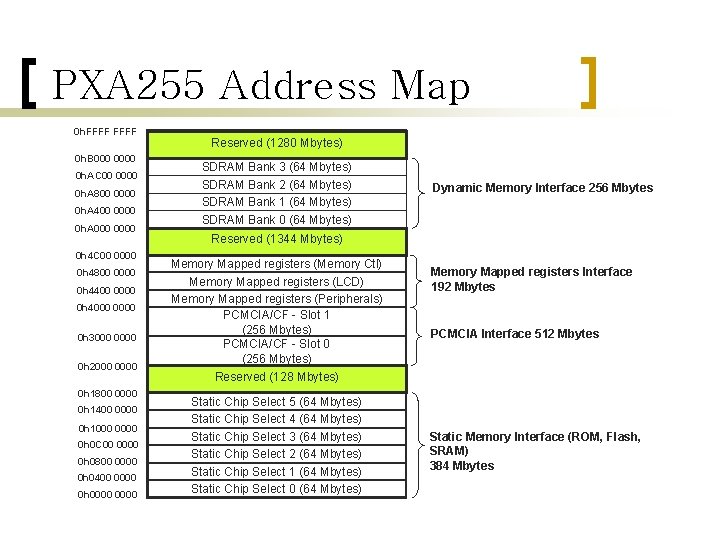
PXA 255 Address Map 0 h. FFFF 0 h. B 0000 0 h. AC 00 0000 0 h. A 800 0000 0 h. A 400 0000 0 h. A 0000 0 h 4 C 00 0000 0 h 4800 0000 0 h 4400 0000 0 h 4000 0 h 3000 0 h 2000 0 h 1800 0000 0 h 1400 0000 0 h 1000 0 h 0 C 00 0000 0 h 0800 0000 0 h 0400 0000 0 h 0000 Reserved (1280 Mbytes) SDRAM Bank 3 (64 Mbytes) SDRAM Bank 2 (64 Mbytes) SDRAM Bank 1 (64 Mbytes) SDRAM Bank 0 (64 Mbytes) Dynamic Memory Interface 256 Mbytes Reserved (1344 Mbytes) Memory Mapped registers (Memory Ctl) Memory Mapped registers (LCD) Memory Mapped registers (Peripherals) PCMCIA/CF - Slot 1 (256 Mbytes) PCMCIA/CF - Slot 0 (256 Mbytes) Memory Mapped registers Interface 192 Mbytes PCMCIA Interface 512 Mbytes Reserved (128 Mbytes) Static Chip Select 5 (64 Mbytes) Static Chip Select 4 (64 Mbytes) Static Chip Select 3 (64 Mbytes) Static Chip Select 2 (64 Mbytes) Static Chip Select 1 (64 Mbytes) Static Chip Select 0 (64 Mbytes) Static Memory Interface (ROM, Flash, SRAM) 384 Mbytes
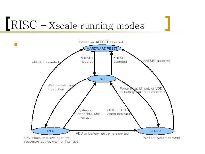
RISC n – Xscale running modes PXA 255 동작모드
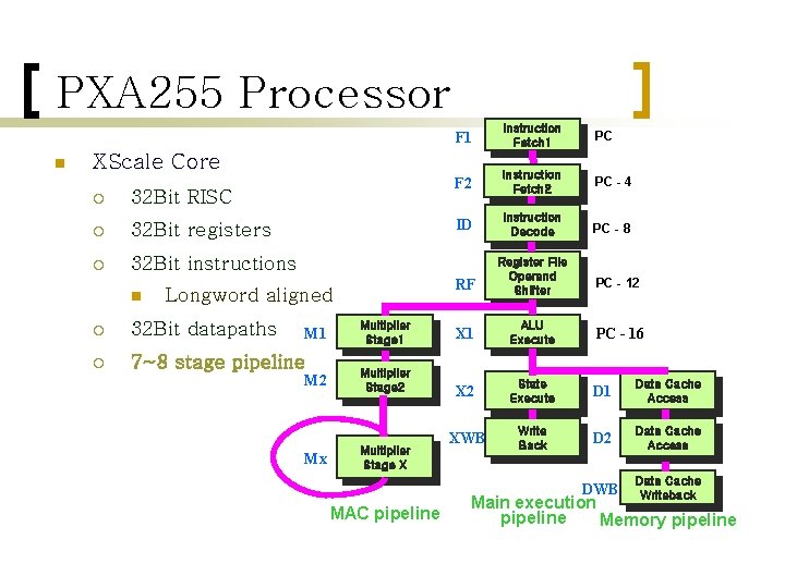
PXA 255 Processor n F 1 Instruction Fetch 1 PC F 2 Instruction Fetch 2 PC - 4 ID Instruction Decode PC - 8 RF Register File Operand Shifter X 1 ALU Execute PC - 16 X 2 State Execute D 1 Data Cache Access XWB Write Back D 2 Data Cache Access DWB Data Cache Writeback XScale Core ¡ 32 Bit RISC ¡ 32 Bit registers ¡ 32 Bit instructions n Longword aligned ¡ 32 Bit datapaths ¡ 7~8 stage pipeline M 1 M 2 Mx Multiplier Stage 1 Multiplier Stage 2 Multiplier Stage X MAC pipeline PC - 12 Main execution pipeline Memory pipeline
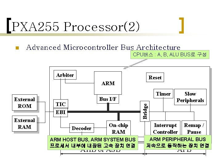
PXA 255 Processor(2) n Advanced Microcontroller Bus Architecture CPU버스 : A, B, ALU BUS로 구성 Arbiter Reset ARM External RAM Bus I/F TIC EBI Slow Peripherals Bridge External ROM Timer Decoder On-chip RAM ARM HOST BUS, ARM SYSTEM BUS 프로세서 내부에 내장된 고속 장치 연결 AHB or ASB Interrupt Controller Remap / Pause ARM PERIPHERAL BUS 저속으로 동작하는 장치 연결 APB
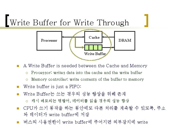
Write Buffer for Write Through Processor Cache DRAM Write Buffer n A Write Buffer is needed between the Cache and Memory ¡ Processor: writes data into the cache and the write buffer ¡ Memory controller: write contents of the buffer to memory n Write buffer is just a FIFO: n Write Buffer는 쓰는 경우의 성능 향상을 위해 존재 ¡ 캐시 메모리는 명령어, 데이터를 읽을 경우의 성능 향상 n CPU가 쓰기 동작을 하는 동안에도 다른 처리를 계속할 수 있도록, 주소 와 데이터가 write buffer에 저장 n 버스의 사용권한이 write buffer에 주어지면 외부장치에 write
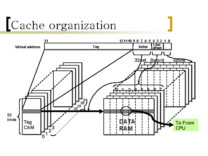
Cache organization 31 Tag Virtual address 12 11 10 9 8 7 6 5 4 3 2 1 0 Line Index offset 32 set 8 word 4 byte 0 1 2 3 4 5 6 7 31 30 29 28 32 lines Tag CAM 0 1 2 3 DATA RAM To From CPU
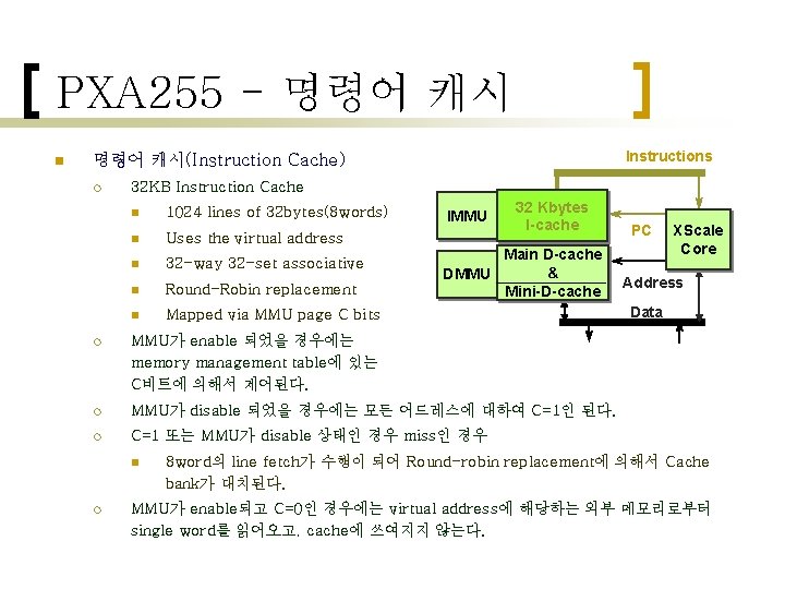
PXA 255 - 명령어 캐시 n Instructions 명령어 캐시(Instruction Cache) ¡ 32 KB Instruction Cache n 1024 lines of 32 bytes(8 words) n Uses the virtual address n 32 -way 32 -set associative n Round-Robin replacement n Mapped via MMU page C bits IMMU 32 Kbytes I-cache Main D-cache & DMMU Mini-D-cache ¡ MMU가 enable 되었을 경우에는 memory management table에 있는 C비트에 의해서 제어된다. ¡ MMU가 disable 되었을 경우에는 모든 어드레스에 대하여 C=1인 된다. ¡ C=1 또는 MMU가 disable 상태인 경우 miss인 경우 n ¡ PC XScale Core Address Data 8 word의 line fetch가 수행이 되어 Round-robin replacement에 의해서 Cache bank가 대치된다. MMU가 enable되고 C=0인 경우에는 virtual address에 해당하는 외부 메모리로부터 single word를 읽어오고, cache에 쓰여지지 않는다.
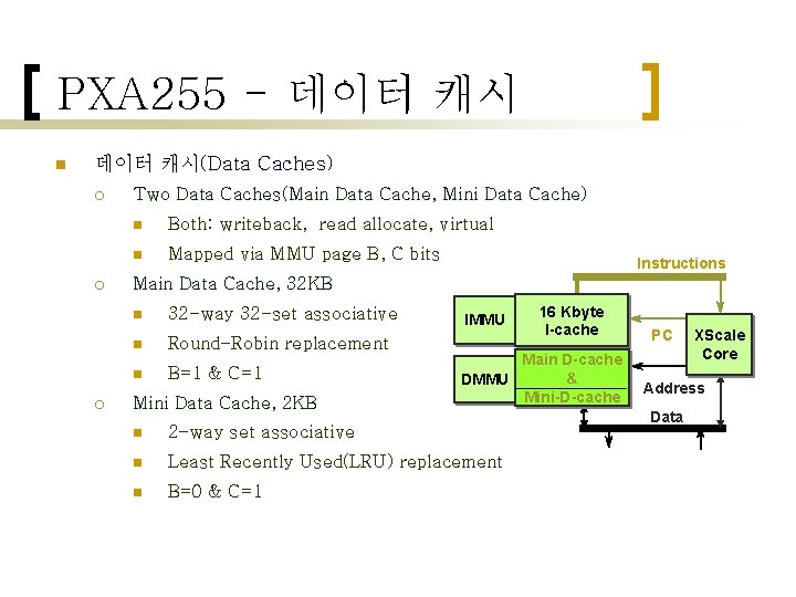
PXA 255 - 데이터 캐시 n 데이터 캐시(Data Caches) ¡ ¡ ¡ Two Data Caches(Main Data Cache, Mini Data Cache) n Both: writeback, read allocate, virtual n Mapped via MMU page B, C bits Instructions Main Data Cache, 32 KB n 32 -way 32 -set associative n Round-Robin replacement n B=1 & C=1 Mini Data Cache, 2 KB IMMU 16 Kbyte I-cache Main D-cache & DMMU Mini-D-cache n 2 -way set associative n Least Recently Used(LRU) replacement n B=0 & C=1 PC XScale Core Address Data

PXA 255 - Read Buffer n PXA 255 Read Buffer v Instructions I-cache PC D-cache & mini-D-cache XScale Core Data prefetcher Ø saves processor waiting Ø load & calculate in parallel Ø for Read-Only data Ø supplements the data cache Address Data Write Buffer 128 Byte Read Buffer System Bus v Under software control Ø Coprocessor 15, register #9 Ø 4 entries, 32 bytes each Ø Loads of 1, 4, 8 words Ø Replace or invalidate data
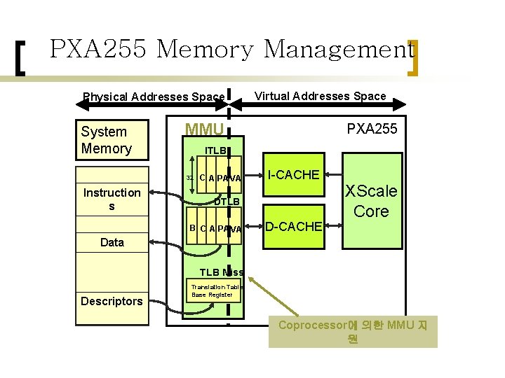
PXA 255 Memory Management Physical Addresses Space System Memory MMU PXA 255 ITLB 32 Instruction s Virtual Addresses Space C A PA VA I-CACHE DTLB B C A PA VA D-CACHE XScale Core Data TLB Miss Descriptors Translation Table Base Register Coprocessor에 의한 MMU 지 원
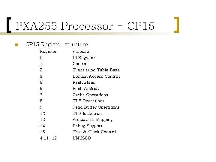
PXA 255 Processor - CP 15 n CP 15 Register structure Register 0 1 2 3 5 6 7 8 9 10 13 14 15 4, 11~12 Purpose ID Register Control Translation Table Base Domain Access Control Fault Staus Fault Address Cache Operations TLB Operations Read Buffer Operations TLB lockdown Process ID Mapping Debug Support Test & Clock Control UNUSED
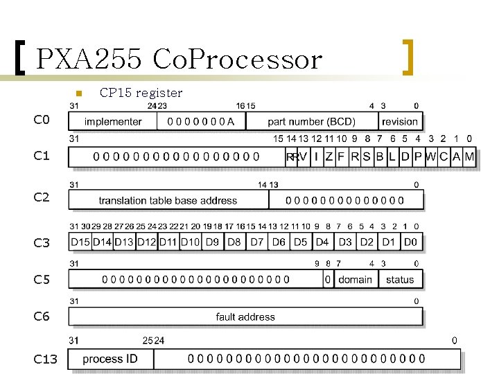
PXA 255 Co. Processor n C 0 C 1 C 2 C 3 C 5 C 6 C 13 CP 15 register
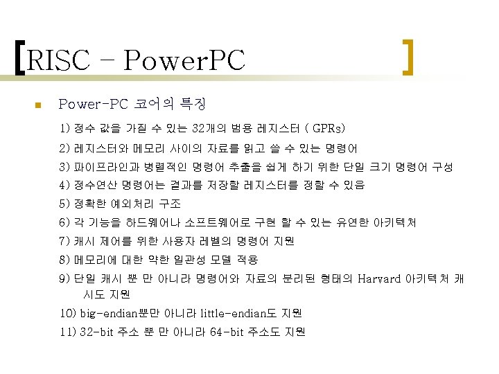
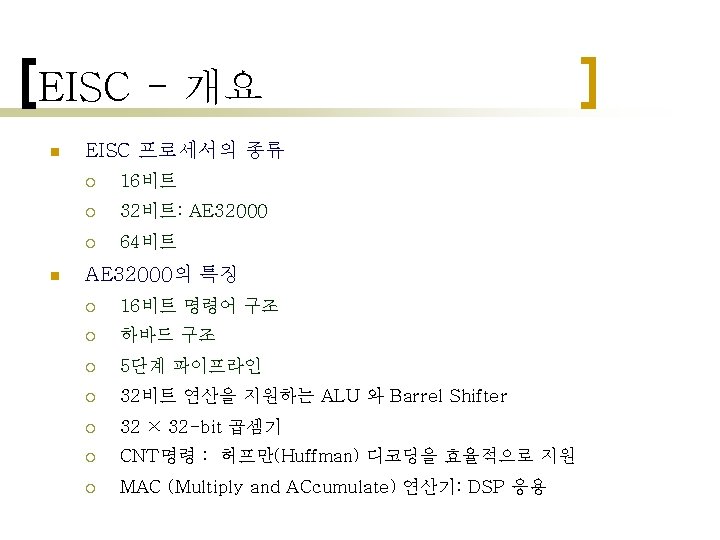
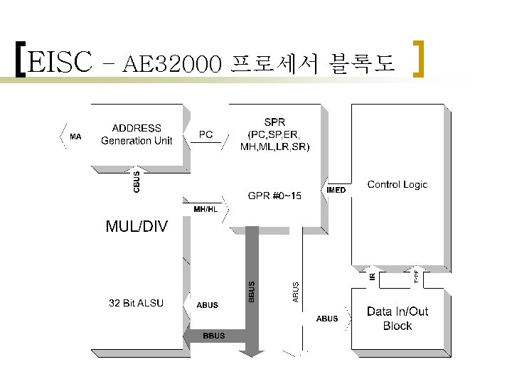
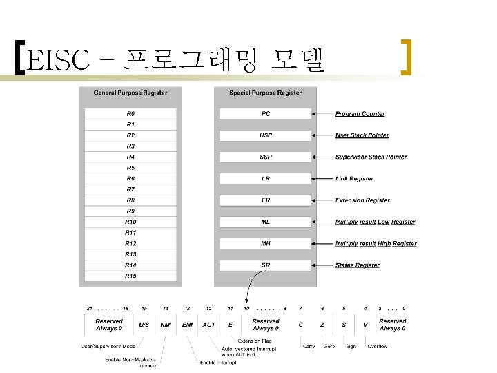
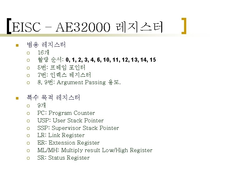
EISC – AE 32000 레지스터 n 범용 레지스터 ¡ ¡ ¡ n 16개 할당 순서: 0, 1, 2, 3, 4, 6, 10, 11, 12, 13, 14, 15 5번: 프레임 포인터 7번: 인덱스 레지스터 8, 9번: Argument Passing 용도. 특수 목적 레지스터 ¡ ¡ ¡ ¡ 9개 PC: Program Counter USP: User Stack Pointer SSP: Supervisor Stack Pointer LR: Link Register ER: Extension Register ML/MH: Multiply result Low/High Register SR: Status Register
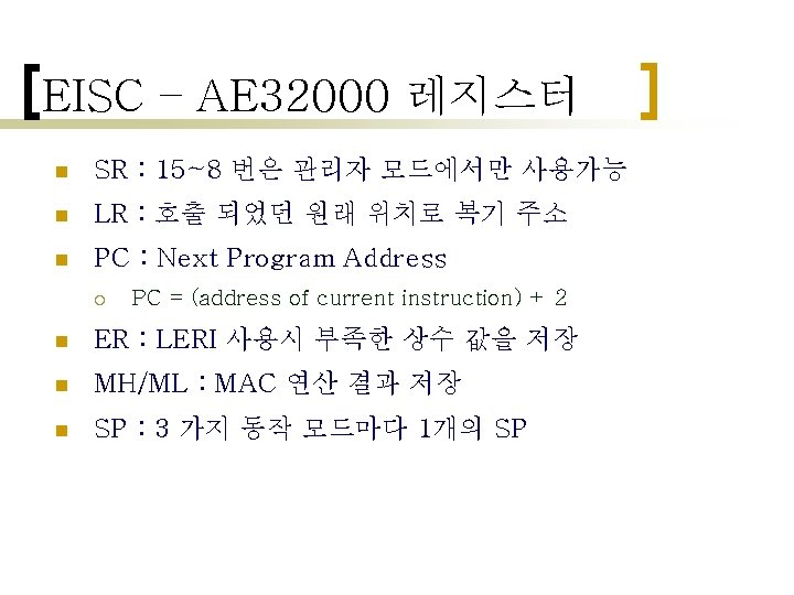
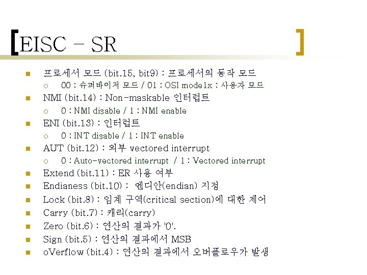
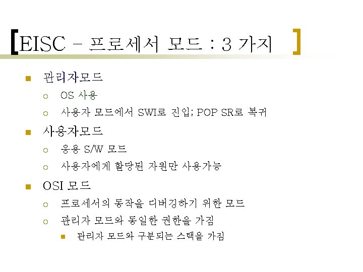
EISC – SR n 프로세서 모드 (bit. 15, bit 9) : 프로세서의 동작 모드 ¡ n NMI (bit. 14) : Non-maskable 인터럽트 ¡ n n n n 0 : INT disable / 1 : INT enable AUT (bit. 12) : 외부 vectored interrupt ¡ n 0 : NMI disable / 1 : NMI enable ENI (bit. 13) : 인터럽트 ¡ n 00 : 슈퍼바이저 모드 / 01 : OSI mode 1 x : 사용자 모드 0 : Auto-vectored interrupt / 1 : Vectored interrupt Extend (bit. 11) : ER 사용 여부 Endianess (bit. 10) : 엔디안(endian) 지정 Lock (bit. 8) : 임계 구역(critical section)에 대한 제어 Carry (bit. 7) : 캐리(carry) Zero (bit. 6) : 연산의 결과가 '0'. Sign (bit. 5) : 연산의 결과에서 MSB o. Verflow (bit. 4) : 연산의 결과에서 오버플로우가 발생
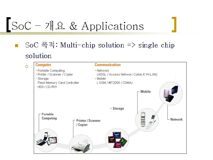
So. C – 개요 & Applications n So. C 목적: Multi-chip solution => single chip solution ¡ 저전력, 소형화, 저가격, 안정성 증가
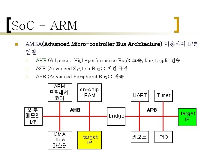
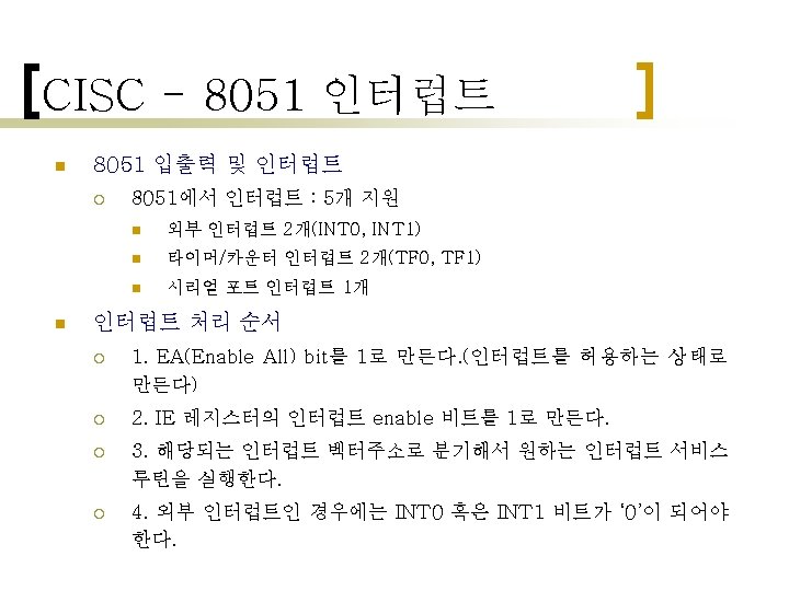
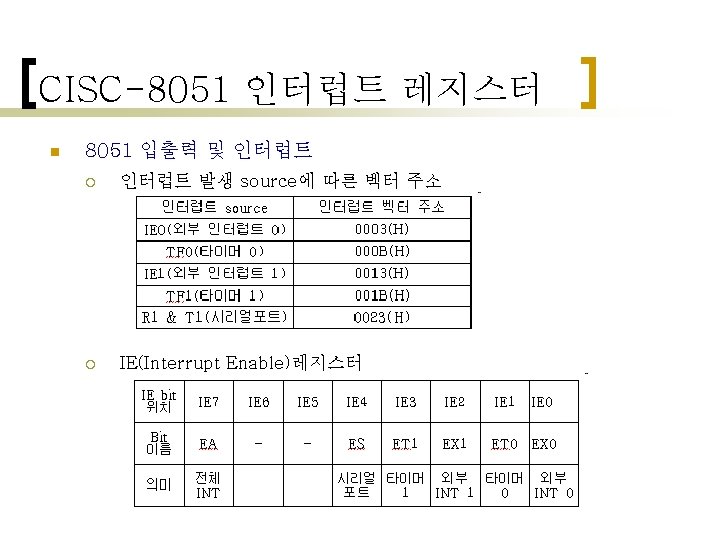
So. C - ARM n AMBA(Advanced Micro-controller Bus Architecture) 이용하여 IP를 연결 ¡ AHB (Advanced High-performance Bus): 고속, burst, split 전송 ¡ ASB (Advanced System Bus) : 이전 규격 ¡ APB (Advanced Peripheral Bus) : 저속
- Slides: 97