AVR ATMEGA 8 MICROCONTROLLER INTRODUCTION ATmega 8 is


 • 32 -pin TQFP (Thin")


 • Port B is an 8 -bit")
 • Port C is an 7 -bit")
 • Port D is an 8 -bit")


- Slides: 21
AVR ATMEGA 8 MICRO-CONTROLLER
INTRODUCTION • ATmega 8 is a 8 -bit microcontroller based on the AVR RISC architecture • By executing powerful instructions in a single clock cycle, the ATmega 8 achieves throughput approaching 1 MIPS per MHz
Contd. . • In order to maximize performance and parallelism, the AVR uses a Harvard architecture- which separates memories and buses for program and data • Instruction in program memory are executed with single level pipelining • This concept enables instructions to be executed in every clock cycle
• • • High-performance 8 bit Microcontroller Up to 16 MIPS Throughput at 16 MHz 32 x 8 General Purpose Working Registers Six ADC channels in PDIP package Internal Calibrated Oscillator
• 28 -pin PDIP (Plastic Dual In-line Package) • 32 -pin TQFP (Thin Quad film Package)
Memory Segments • 8 K Bytes of Flash program memory • 512 Bytes EEPROM (Electrically Erasable Programmable Read Only Memory) • 1 K Byte Internal RAM (Random Access Memory)
Contd. . • Write/Erase Cycles: 10, 000 Flash/100, 000 EEPROM • Data retention: 20 years at 85°C/100 years at 25°C
Pin Out
• VCC Digital supply voltage • GND Ground • RESET A low level on this pin for longer than the minimum pulse length will generate a reset, even if the clock is not running • AREF The analog reference pin for the A/D Converter
Contd. . • AVCC The supply voltage pin for the A/D Converter
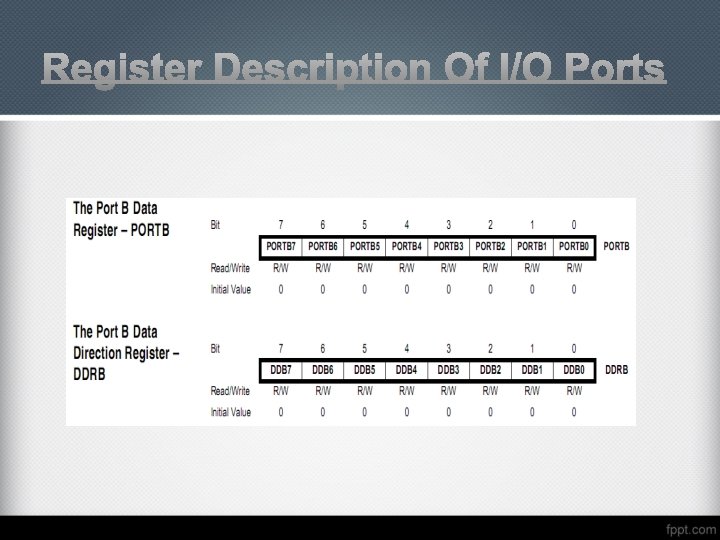
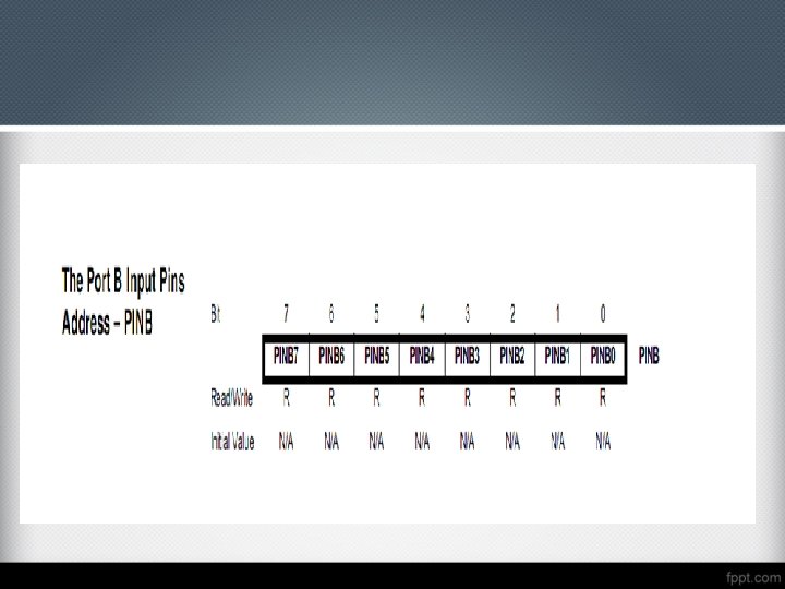
Ports • Three ports i. e Port. B, Port. C, Port. D • Three registers associated with every port Ø DDRx – Data Direction Register Ø PINx – Port input Ø PORTx- Port output *Note – ‘x’ is subscript and could be either of B, C, D
Port B (PB 7. . PB 0) • Port B is an 8 -bit bi-directional I/O port • Can be used either as a input port or as output port ( direction must be specified in programming)
Port C (PC 5. . PC 0) • Port C is an 7 -bit bi-directional I/O port • Can be used either as a input port or as output port ( direction must be specified in programming).
Port D (PD 7. . PD 0) • Port D is an 8 -bit bi-directional I/O port • Can be used either as a input port or as output port ( direction must be specified in coding)
Contd. .
Contd. .
Contd. .
Contd. .
Thank you…