AV Open circuit voltage gain AV vi Open
- Slides: 10

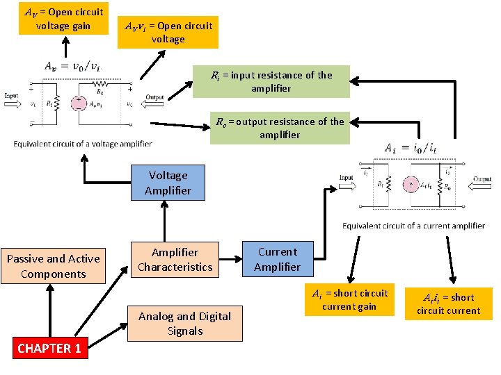
AV = Open circuit voltage gain AV vi = Open circuit voltage Ri = input resistance of the amplifier Ro = output resistance of the amplifier Voltage Amplifier Passive and Active Components Amplifier Characteristics Current Amplifier Ai = short circuit Analog and Digital Signals CHAPTER 1 current gain Ai ii = short circuit current

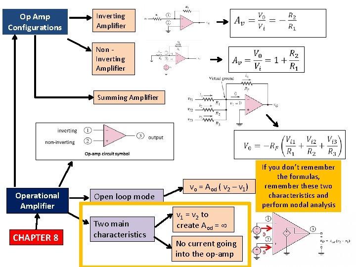
Op Amp Configurations Inverting Amplifier Non - Inverting Amplifier Summing Amplifier Operational Amplifier CHAPTER 8 Open loop mode Two main characteristics vo = Aod ( v 2 – v 1) v 1 = v 2 to create Aod = No current going into the op-amp If you don’t remember the formulas, remember these two characteristics and perform nodal analysis

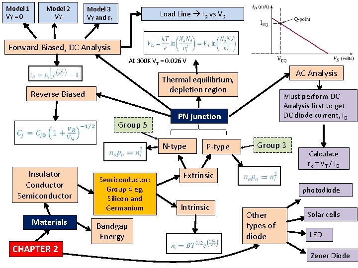
Model 1 V = 0 Model 2 V Model 3 V and rf Load Line ID vs VD Forward Biased, DC Analysis At 300 K VT = 0. 026 V Reverse Biased Group 5 Materials CHAPTER 2 Semiconductor: Group 4 eg. Silicon and Germanium Bandgap Energy Must perform DC Analysis first to get DC diode current, ID PN junction N-type Insulator Conductor Semiconductor AC Analysis Thermal equilibrium, depletion region P-type Group 3 Calculate rd = VT / ID Extrinsic photodiode Intrinsic Other types of diode Solar cells LED Zener Diode

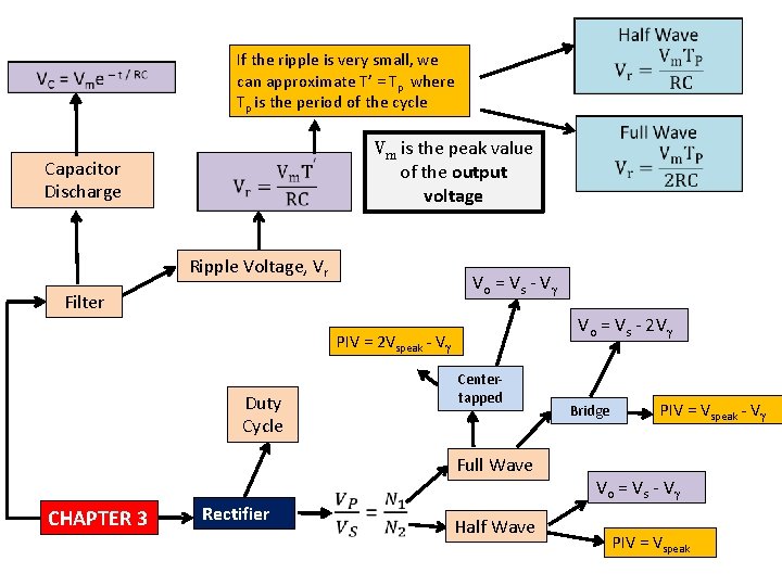
If the ripple is very small, we can approximate T’ = Tp where Tp is the period of the cycle Capacitor Discharge Vm is the peak value of the output voltage Ripple Voltage, Vr Vo = Vs - V Filter Vo = Vs - 2 V PIV = 2 Vspeak - V Duty Cycle Centertapped Full Wave CHAPTER 3 Rectifier Half Wave Bridge PIV = Vspeak - V Vo = Vs - V PIV = Vspeak

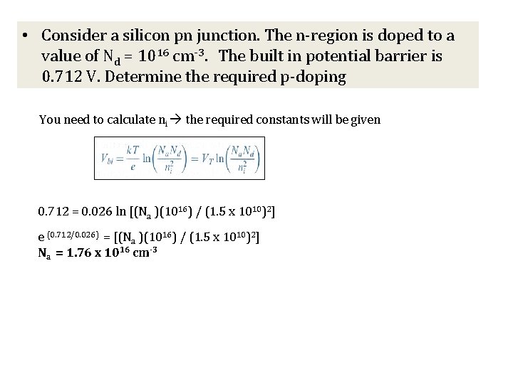
• Consider a silicon pn junction. The n-region is doped to a value of Nd = 1016 cm-3. The built in potential barrier is 0. 712 V. Determine the required p-doping You need to calculate ni the required constants will be given 0. 712 = 0. 026 ln [(Na )(1016) / (1. 5 x 10¹⁰)2] e (0. 712/0. 026) = [(Na )(1016) / (1. 5 x 10¹⁰)2] Na = 1. 76 x 1016 cm-3

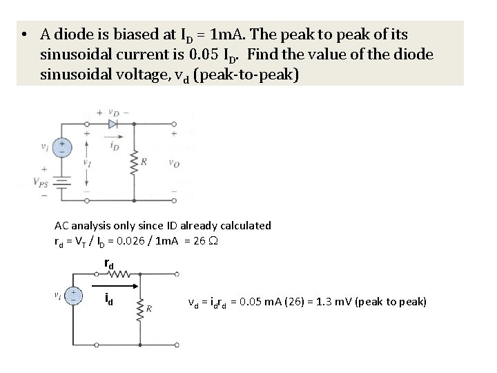
• A diode is biased at ID = 1 m. A. The peak to peak of its sinusoidal current is 0. 05 ID. Find the value of the diode sinusoidal voltage, vd (peak-to-peak) AC analysis only since ID already calculated rd = VT / ID = 0. 026 / 1 m. A = 26 rd id vd = idrd = 0. 05 m. A (26) = 1. 3 m. V (peak to peak)

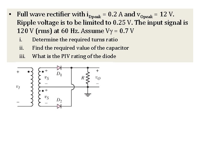
• Full wave rectifier with i. Dpeak = 0. 2 A and v. Opeak = 12 V. Ripple voltage is to be limited to 0. 25 V. The input signal is 120 V (rms) at 60 Hz. Assume V = 0. 7 V i. iii. Determine the required turns ratio Find the required value of the capacitor What is the PIV rating of the diode

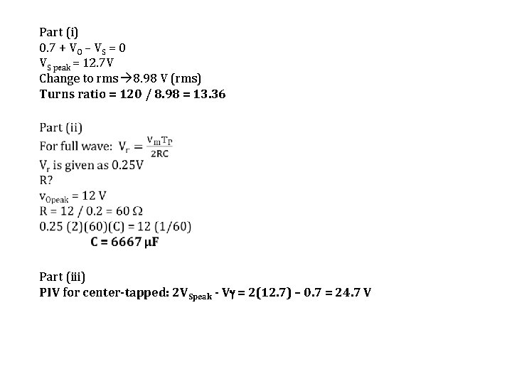
Part (i) 0. 7 + VO – VS = 0 VS peak = 12. 7 V Change to rms 8. 98 V (rms) Turns ratio = 120 / 8. 98 = 13. 36 Part (iii) PIV for center-tapped: 2 VSpeak - V = 2(12. 7) – 0. 7 = 24. 7 V

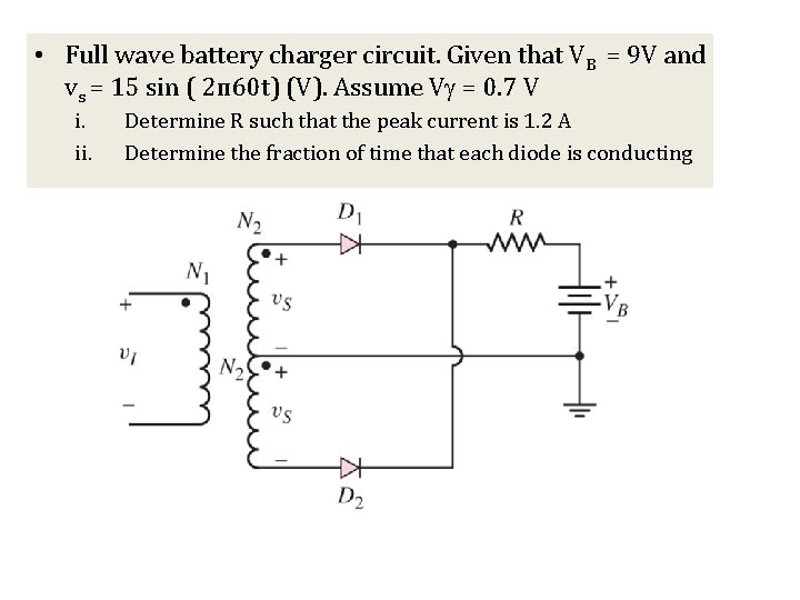
• Full wave battery charger circuit. Given that VB = 9 V and vs = 15 sin ( 2ᴨ 60 t) (V). Assume V = 0. 7 V i. ii. Determine R such that the peak current is 1. 2 A Determine the fraction of time that each diode is conducting

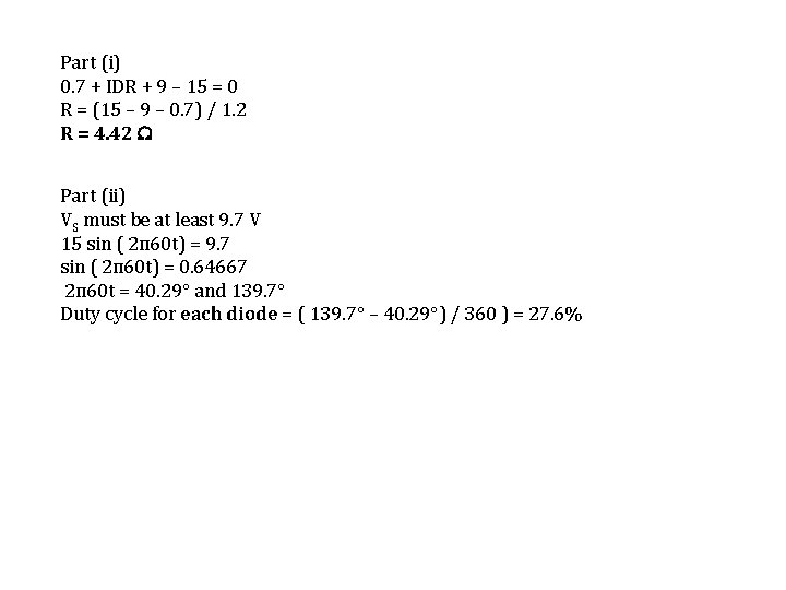
Part (i) 0. 7 + IDR + 9 – 15 = 0 R = (15 – 9 – 0. 7) / 1. 2 R = 4. 42 Part (ii) VS must be at least 9. 7 V 15 sin ( 2ᴨ 60 t) = 9. 7 sin ( 2ᴨ 60 t) = 0. 64667 2ᴨ 60 t = 40. 29 and 139. 7 Duty cycle for each diode = ( 139. 7 – 40. 29 ) / 360 ) = 27. 6%