Atomiclayer CVD ALCVD Fluidized bed ALD reactor designed
 Fluidized bed ALD reactor designed for deposition on porous samples.")
Atomic-layer CVD (ALCVD) Fluidized bed ALD reactor designed for deposition on porous samples.
")
Atomic-layer CVD (ALCVD)
")
Atomic-layer CVD (ALCVD)
")
Atomic-layer CVD (ALCVD)
 This process uses a hot filament to chemically decompose the")
Hot filament CVD (HFCVD) This process uses a hot filament to chemically decompose the source gasses. The filament temperature and substrate temperature thus are independently controlled, allowing colder temperatures for better absorption rates at the substrate and higher temperatures necessary for decomposition of precursors to free radicals at the filament. It is also known as catalytic CVD (Cat-CVD) or more commonly, initiated CVD (i. CVD).
 (a) Schematic diagram of the HFCVD used, (b) Raman spectra")
Hot filament CVD (HFCVD) (a) Schematic diagram of the HFCVD used, (b) Raman spectra of the graphene obtained, (c) picture of the graphene transferred on Si. O 2 substrate, and (d) Raman mapping of a selected area of the hydrogenated graphene. (a) SEM micrograph of graphene films on Cu surface with optical photograph shown in the inset https: //www. intechopen. com/books/chemical-vapor-deposition-recent-advances-and-applications-in-optical-solar-cells-and-solid-state-devices/hot-filamentchemical-vapor-deposition-enabling-the-scalable-synthesis-of-bilayer-graphene-and-other
 This CVD process is based on metalorganic precursors. Zn(CH")
Metalorganic chemical vapor deposition (MOCVD) This CVD process is based on metalorganic precursors. Zn(CH 2 CH 3)2 / H 2 O / Ar Geometry of the Zn. O-MOCVD reactor. Applied Thermal Engineering Volume 136, 25 May 2018, Pages 108 -117
 This CVD process is based on metalorganic precursors. Applied")
Metalorganic chemical vapor deposition (MOCVD) This CVD process is based on metalorganic precursors. Applied Thermal Engineering Volume 136, 25 May 2018, Pages 108 -117
 This process uses UV light to stimulate chemical reactions. Under certain")
Photo-initiated CVD (PICVD) This process uses UV light to stimulate chemical reactions. Under certain conditions, photo initiated CVD can be operated at or near atmospheric pressure.
 This CVD process uses lasers to heat spots or")
Laser Chemical vapor deposition (LCVD) This CVD process uses lasers to heat spots or lines on a substrate in semiconductor applications. In Micro Electro-Mechanical Systems (MEMS) and in fiber production the lasers are used rapidly to break down the precursor gas to build up a solid structure. Laser induced temperature can exceed 2000 °C.
")
Laser Chemical vapor deposition (LCVD)
 – This CVD process uses heating lamps or other methods")
Rapid thermal CVD (RTCVD) – This CVD process uses heating lamps or other methods to rapidly heat the wafer substrate. Heating only the substrate rather than the gas or chamber walls helps reduce unwanted gas-phase reactions that can lead to particle formation. Hybrid Physical-Chemical Vapor Deposition (HPCVD) – This process involves both chemical decomposition of precursor gas and vaporization of a solid source.

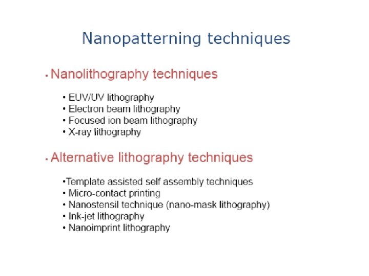
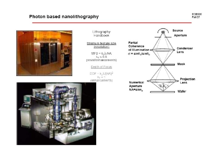
Nanolithography Lithography uses simple chemical processes to create an image. The printing is from a stone (lithographic limestone) or a metal plate with a smooth surface. Nanolithography deals with the engineering (etching, writing, printing) of nanometerscale structures. All nanolithographic techniques can be separated into two categories: - etch away molecules leaving behind the desired structure; - directly write the desired structure to a surface. . • in the fabrication of integrated circuits (IC) • information storage devices • fabrication of micro-electromechanical systems (MEMS) • minute sensors • nano and microfluidic devices • biochips • photonics
 There are two main LIGA-fabrication technologies,")
LIGA Lithographie, Galvanoformung, Abformung (Lithography, Electroplating, and Molding) There are two main LIGA-fabrication technologies, X-Ray LIGA, which uses Xrays produced by a synchrotron to create high-aspect ratio structures, and UV LIGA, a more accessible method which uses ultraviolet light to create structures with relatively low aspect ratios. high aspect ratios on the order of 100: 1 parallel side walls with a flank angle on the order of 89. 95° smooth side walls with suitable for optical mirrors structural heights from tens of micrometers to several millimeters structural details on the order of micrometers over distances of centimeters SEM picture of a polymer LIGA structure made by moulding. Smallest polymer width is 6 µm; polymer height is 120 µm, the aspect ratio is, therefore, 20.

The field of nanolithography was born out of the need to increase the number of transistors in an integrated circuit in order to maintain Moore's Law.
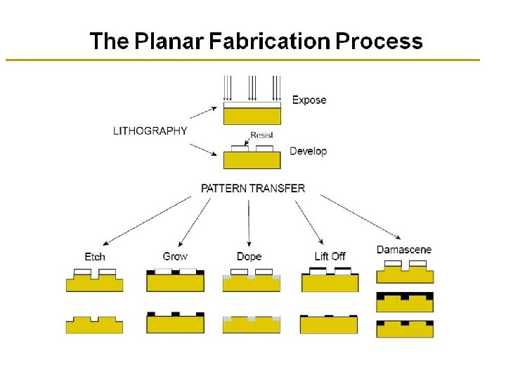
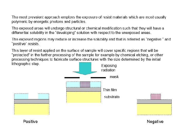

Resists must have the necessary mechanical properties to be useful in the subsequent processing of the sample. Considering its chemical characteristics, resists can be characterized in two categories: Conventional photoresists: the energy of the radiation in the exposure directly converts into a chemical reaction in the resist. Chemically amplified: an intermediate catalytic process happens prior to development. Polymethylmethacrylate (PMMA) is a positive tone resist that can be activated with UV light, X -rays, electrons or ions. Molecular weights form 500 k to 1000 k with slightly different properties.

Nano. Stencil lithography

Nano. Stencil lithography
- Slides: 27