Atomic scale Design of Nanostructures Jerzy Bernholc North

Atomic scale Design of Nanostructures Jerzy Bernholc North Carolina State Univ. , Raleigh, NC 27695 -8202 and Oak Ridge National Laboratories, TN 37831 -6359 I. Nanotube-cluster-based molecular sensors II. Piezo- and ferroelectric materials • Boron nitride nanotubes • Ferroelectric polymers and prediction of new ones with 100% improved piezo- and ferroelectric properties III. Optical signatures of surface structures • • Feedback control during growth possible (with monolayer resolution) Reconstruction patterns, nanowires on surfaces IV. Summary Collaborators: M. Buongiorno Nardelli, W. Lu, V. Meunier, S. Nakhmanson, W. G. Schmidt, S. Wang and Q. Zhao NC STATE UNIVERSITY
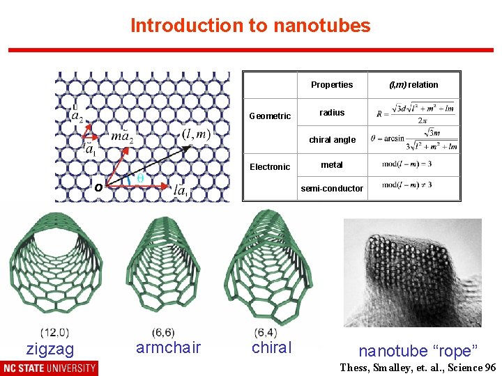
Introduction to nanotubes Properties Geometric (l, m) relation radius chiral angle Electronic o zigzag metal semi-conductor armchair chiral nanotube “rope” Thess, Smalley, et. al. , Science 96
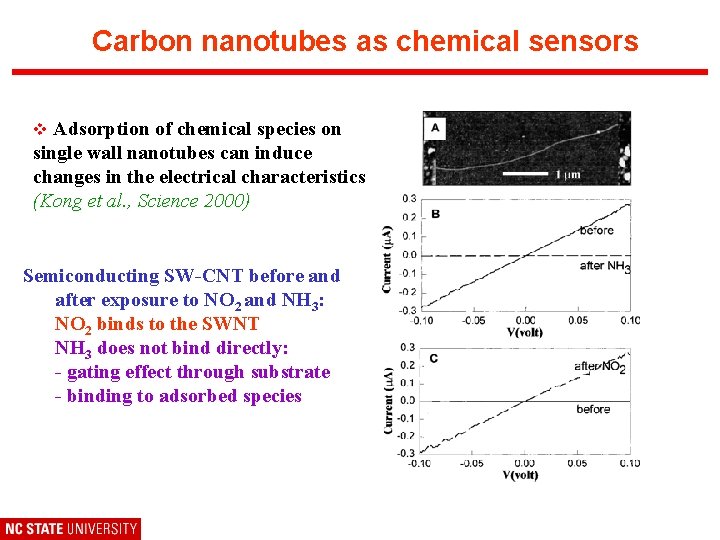
Carbon nanotubes as chemical sensors v Adsorption of chemical species on single wall nanotubes can induce changes in the electrical characteristics (Kong et al. , Science 2000) Semiconducting SW-CNT before and after exposure to NO 2 and NH 3: NO 2 binds to the SWNT NH 3 does not bind directly: - gating effect through substrate - binding to adsorbed species
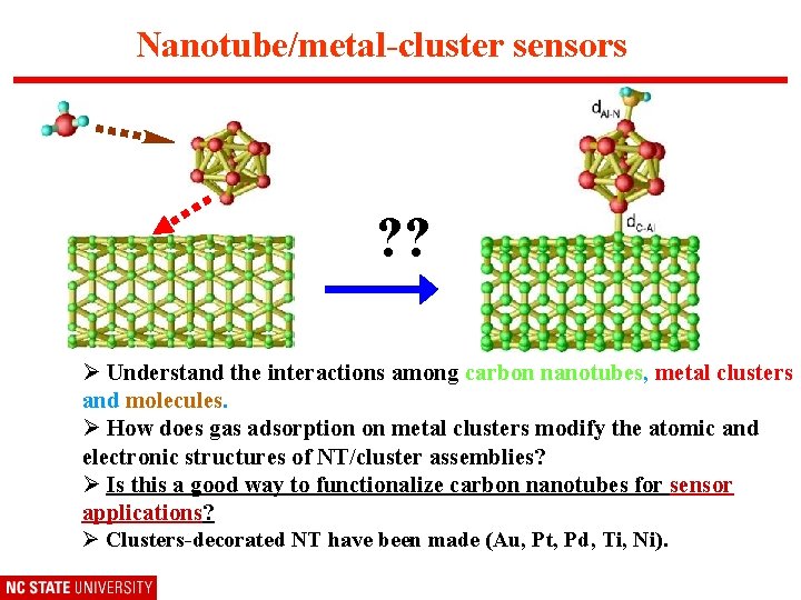
Nanotube/metal-cluster sensors ? ? Ø Understand the interactions among carbon nanotubes, metal clusters and molecules. Ø How does gas adsorption on metal clusters modify the atomic and electronic structures of NT/cluster assemblies? Ø Is this a good way to functionalize carbon nanotubes for sensor applications? Ø Clusters-decorated NT have been made (Au, Pt, Pd, Ti, Ni).
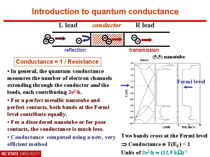
Introduction to quantum conductance L lead --- conductor reflection Conductance = 1 / Resistance -- R lead -transmission (5, 5) nanotube • In general, the quantum conductance measures the number of electron channels Fermi level extending through the conductor and the leads, each contributing 2 e 2/h. • For a perfect metallic nanotube and perfect contacts, both bands at the Fermi level contribute equally. • For a disordered nanotube or for poor contacts, the conductance is much less. • Conductance computed using a new, very Two bands cross at the Fermi level efficient method Conductance T(EF) = 2 Units of 2 e 2/h (12. 9 k )-1
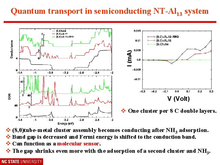
I (m. A) Quantum transport in semiconducting NT-Al 13 system V (Volt) v One cluster per 8 C double layers. v (8, 0)tube-metal cluster assembly becomes conducting after NH 3 adsorption. v Band gap is decreased and Fermi energy is shifted to the conduction band. v Can function as a molecular sensor. v The gap shrinks even more with the adsorption of a second cluster and NH 3.
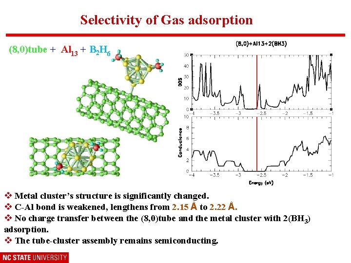
Selectivity of Gas adsorption (8, 0)tube + Al 13 + B 2 H 6 v Metal cluster’s structure is significantly changed. v C-Al bond is weakened, lengthens from 2. 15 Å to 2. 22 Å. v No charge transfer between the (8, 0)tube and the metal cluster with 2(BH 3) adsorption. v The tube-cluster assembly remains semiconducting.
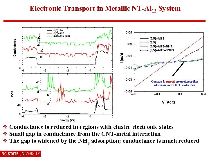
I (m. A) Electronic Transport in Metallic NT-Al 13 System Current is zeroed upon adsorption of one or more NH 3 molecules V (Volt) v Conductance is reduced in regions with cluster electronic states v Small gap in conductance from the CNT-metal interaction v The gap is widened by the NH 3 adsorption; conductance is much reduced
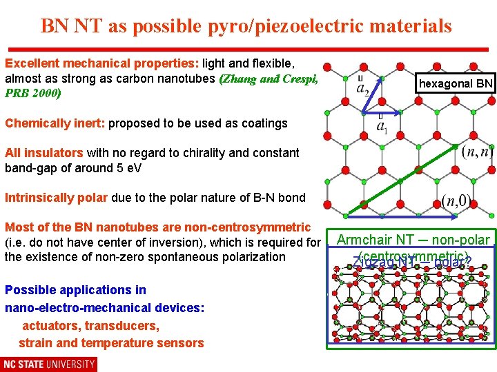
BN NT as possible pyro/piezoelectric materials Excellent mechanical properties: light and flexible, almost as strong as carbon nanotubes (Zhang and Crespi, PRB 2000) hexagonal BN Chemically inert: proposed to be used as coatings All insulators with no regard to chirality and constant band-gap of around 5 e. V Intrinsically polar due to the polar nature of B-N bond Most of the BN nanotubes are non-centrosymmetric (i. e. do not have center of inversion), which is required for the existence of non-zero spontaneous polarization Possible applications in nano-electro-mechanical devices: actuators, transducers, strain and temperature sensors Armchair NT ─ non-polar (centrosymmetric) Zigzag NT ─ polar?
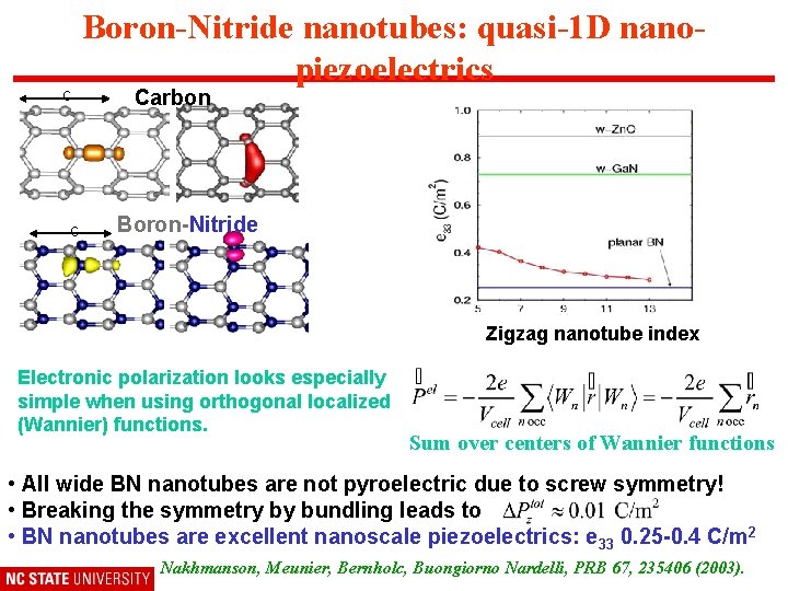
c c Boron-Nitride nanotubes: quasi-1 D nanopiezoelectrics Carbon Boron-Nitride Zigzag nanotube index Electronic polarization looks especially simple when using orthogonal localized (Wannier) functions. Sum over centers of Wannier functions • All wide BN nanotubes are not pyroelectric due to screw symmetry! • Breaking the symmetry by bundling leads to • BN nanotubes are excellent nanoscale piezoelectrics: e 33 0. 25 -0. 4 C/m 2 Nakhmanson, Meunier, Bernholc, Buongiorno Nardelli, PRB 67, 235406 (2003).
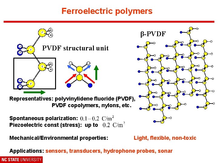
Ferroelectric polymers β-PVDF structural unit Representatives: polyvinylidene fluoride (PVDF), PVDF copolymers, nylons, etc. Spontaneous polarization: Piezoelectric const (stress): up to Mechanical/Environmental properties: Light, flexible, non-toxic Applications: sensors, transducers, hydrophone probes, sonar
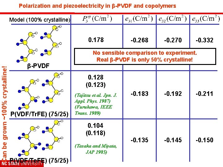
Polarization and piezoelectricity in β-PVDF and copolymers Model (100% crystalline) Can be grown ~100% crystalline! 0. 178 β-PVDF -0. 268 -0. 270 -0. 332 No sensible comparison to experiment. Real β-PVDF is only 50% crystalline! 0. 128 (0. 123) P(VDF/Tr. FE) (75/25) (Tajitsu et al. Jpn. J. Appl. Phys. 1987) (Furukawa, IEEE Trans. 1989) -0. 183 -0. 192 -0. 211 -0. 135 -0. 145 -0. 150 0. 104 (0. 118) (Tasaka and Miyata, JAP 1985) P(VDF/Te. FE) (75/25)
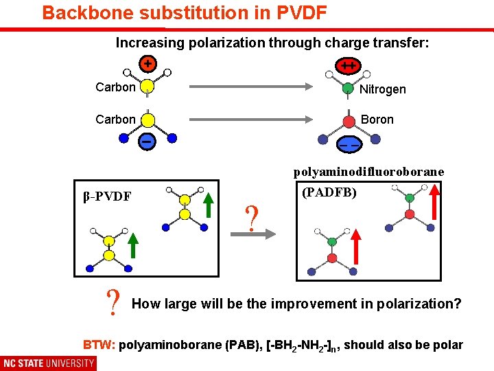
Backbone substitution in PVDF Increasing polarization through charge transfer: + ++ Carbon Nitrogen Carbon Boron – –– polyaminodifluoroborane β-PVDF ? ? (PADFB) How large will be the improvement in polarization? BTW: polyaminoborane (PAB), [-BH 2 -NH 2 -]n, should also be polar
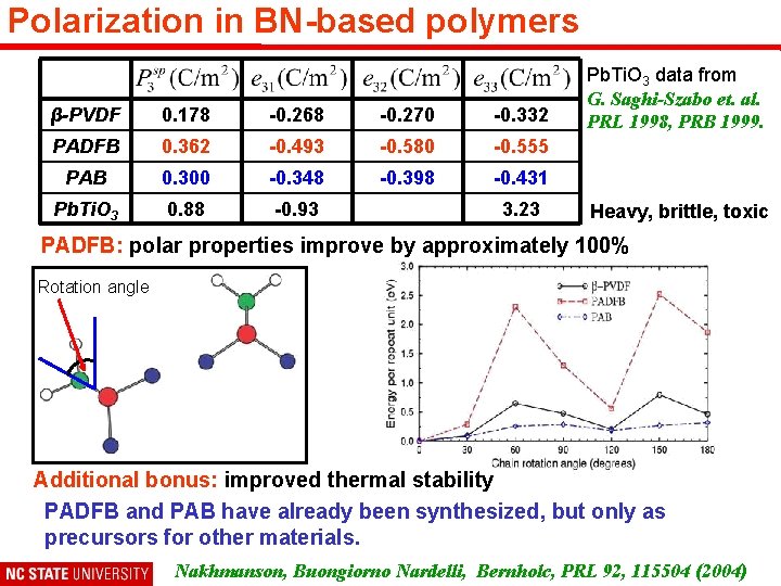
Polarization in BN-based polymers β-PVDF 0. 178 -0. 268 -0. 270 -0. 332 PADFB 0. 362 -0. 493 -0. 580 -0. 555 PAB 0. 300 -0. 348 -0. 398 -0. 431 Pb. Ti. O 3 0. 88 -0. 93 3. 23 Pb. Ti. O 3 data from G. Saghi-Szabo et. al. PRL 1998, PRB 1999. Heavy, brittle, toxic PADFB: polar properties improve by approximately 100% Rotation angle Additional bonus: improved thermal stability PADFB and PAB have already been synthesized, but only as precursors for other materials. Nakhmanson, Buongiorno Nardelli, Bernholc, PRL 92, 115504 (2004)
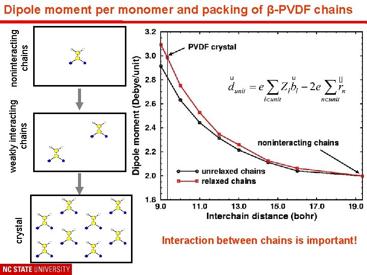
crystal weakly interacting chains noninteracting chains Dipole moment per monomer and packing of β-PVDF chains Interaction between chains is important!
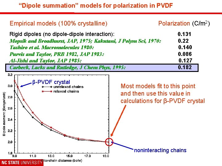
“Dipole summation” models for polarization in PVDF Empirical models (100% crystalline) Polarization (C/m 2) Rigid dipoles (no dipole-dipole interaction): Mopsik and Broadhurst, JAP, 1975; Kakutani, J Polym Sci, 1970: Tashiro et al. Macromolecules 1980: Purvis and Taylor, PRB 1982, JAP 1983: Al-Jishi and Taylor, JAP 1985: Carbeck, Lacks and Rutledge, J Chem Phys, 1995: β-PVDF crystal 0. 131 0. 22 0. 140 0. 086 0. 127 0. 182 Most models fit to this point and then use this value in calculations for β-PVDF crystal noninteracting chains
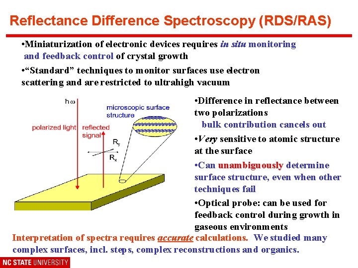
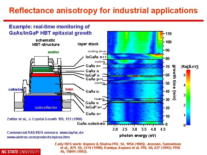
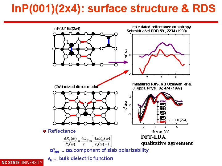
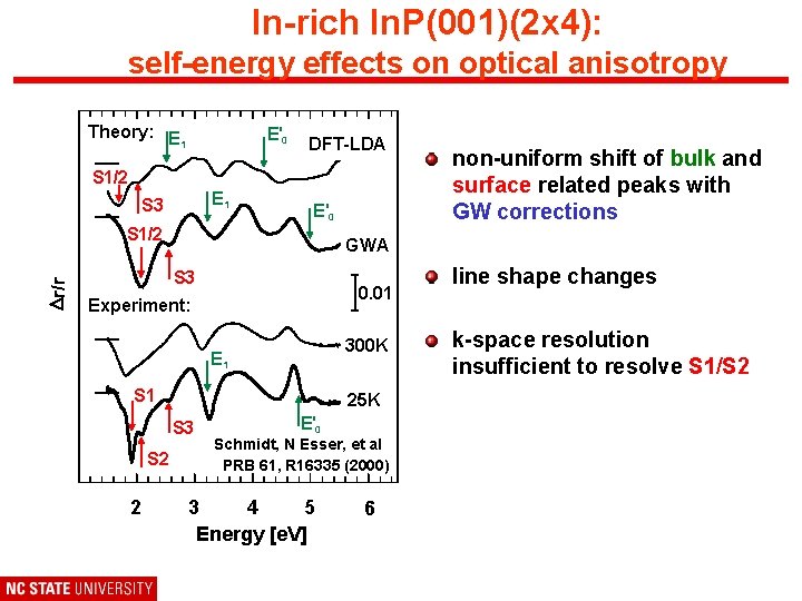
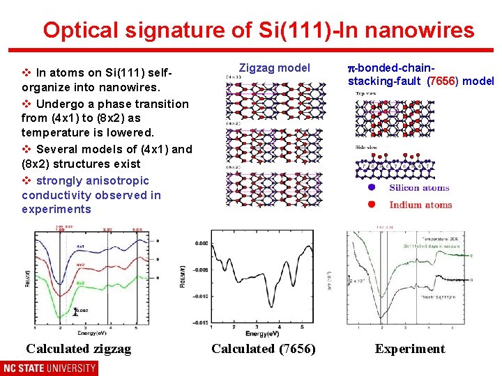
Reflectance Difference Spectroscopy (RDS/RAS) • Miniaturization of electronic devices requires in situ monitoring and feedback control of crystal growth • “Standard” techniques to monitor surfaces use electron scattering and are restricted to ultrahigh vacuum • Difference in reflectance between two polarizations bulk contribution cancels out • Very sensitive to atomic structure at the surface • Can unambiguously determine surface structure, even when other techniques fail • Optical probe: can be used for feedback control during growth in gaseous environments Interpretation of spectra requires accurate calculations. We studied many complex surfaces, incl. steps, complex reconstructions and organics.
Reflectance anisotropy for industrial applications Example: real-time monitoring of Ga. As/In. Ga. P HBT epitaxial growth schematic HBT-structure 110 100 layer stack 90 cooling down emitter In. Ga. As n++ 80 cooling 70 60 cooling base collector 50 Ga. As n- 40 heating 30 Ga. As n In. Ga. P n+ subcollector |Re{D r/r}| 20 Ga. As n+ 10 Zettler et al. , J. Crystal Growth 195, 151 (1998) Ga. As-substrate Commercial RAS/RDS sensors: www. laytec. de www. aixtron. com/products/epiras. htm growth time (min) Ga. As n+ Ga. As n In. Ga. P n Ga. As p++ 2. 0 2. 5 3. 0 3. 5 4. 0 0 4. 5 photon energy (e. V) Early RDS work: Aspnes & Studna PRL 54, 1956 (1985); Jonsson, Samuelson et al. , APL 56, 2414 (1990); Kamiya, Aspnes et al. PRL 68, 627 (1992); PRB 46, 15894 (1992). 5 4 3 2 1 0
In. P(001)(2 x 4): surface structure & RDS calculated reflectance anisotropy Schmidt et al. PRB 59 , 2234 (1999) In. P(001)a 2(2 x 4) 2 10 Dr/r 1 0 -1 2 4 3 measured RAS, KB Ozanyan et al. J. Appl. Phys. 82, 474 (1997) (2 x 4) mixed-dimer model 3 10 Dr/r 2 0 -2 RHEED (2 x 4) Reflectance 2 4 3 Energy [e. V] 5 DFT-LDA qualitative agreement asaa. . . aa component of slab polarizability eb. . . bulk dielectric function
In-rich In. P(001)(2 x 4): self-energy effects on optical anisotropy Theory: E 1 E'0 DFT-LDA S 1/2 E 1 S 3 E'0 Dr/r S 1/2 GWA S 3 0. 01 Experiment: 300 K E 1 S 1 25 K S 3 S 2 2 non-uniform shift of bulk and surface related peaks with GW corrections E'0 Schmidt, N Esser, et al PRB 61, R 16335 (2000) 3 4 5 Energy [e. V] 6 line shape changes k-space resolution insufficient to resolve S 1/S 2
Optical signature of Si(111)-In nanowires v In atoms on Si(111) selforganize into nanowires. v Undergo a phase transition from (4 x 1) to (8 x 2) as temperature is lowered. v Several models of (4 x 1) and (8 x 2) structures exist v strongly anisotropic conductivity observed in experiments Calculated zigzag Zigzag model Calculated (7656) p-bonded-chainstacking-fault (7656) model Experiment

Si/organics surface structures Organics on Si can lead to novel sensors and detectors Cyclopentene monolayer can be used to passivate the Si surface It is a starting point for DNA attachment T. Strother, R. J. Hamers and L. M. Smith, Nucleic Acids Research, 28, 3535 (2000) DNA electrophoresis on a Si surface. N. Pernodet et al, PRL 85, 5651(2000). A new opportunity for silicon-based microelectronics J. T. Yates Jr. , Science 279, 335 (1998). Ordered array of organic molecules (cyclopentene) shows a strong optical anisotropy
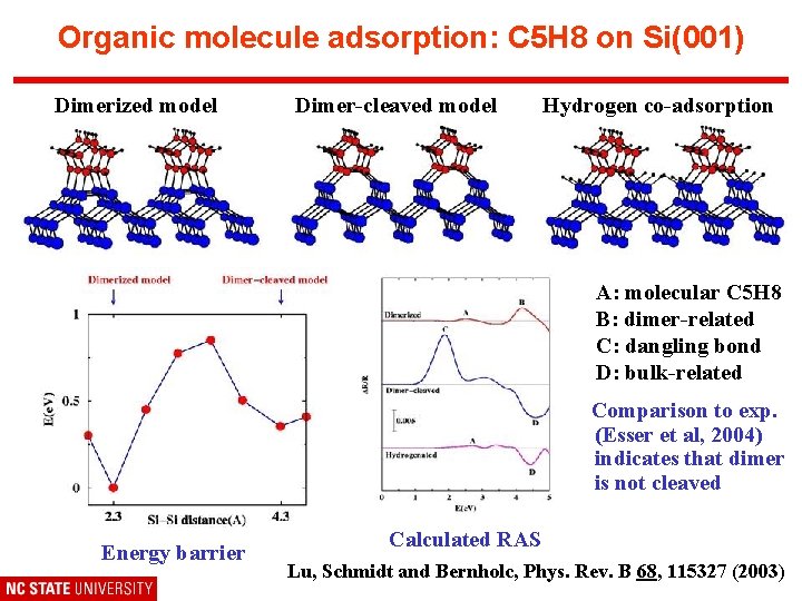
Organic molecule adsorption: C 5 H 8 on Si(001) Dimerized model Dimer-cleaved model Hydrogen co-adsorption A: molecular C 5 H 8 B: dimer-related C: dangling bond D: bulk-related Comparison to exp. (Esser et al, 2004) indicates that dimer is not cleaved Energy barrier Calculated RAS Lu, Schmidt and Bernholc, Phys. Rev. B 68, 115327 (2003)

Summary q Nanotube-cluster structures as ultrasensitive chemical sensors v Potential for detection of specific molecules q Piezo- and ferroelectric materials v Boron nitride nanotubes are excellent piezoelectrics, but are non-polar v Prediction of new, BN-based polymers with 100% improved properties q Building novel materials one layer at a time v Real-time optical monitoring and feedback control of growth v Nanowires on surfaces v Semiconductor/organic interfaces for nano/bio structures

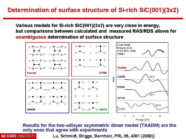
Determination of surface structure of Si-rich Si. C(001)(3 x 2) Various models for Si-rich Si. C(001)(3 x 2) are very close in energy, but comparisons between calculated and measured RAS/RDS allows for unambiguous determination of surface structure Results for the two-adlayer asymmetric dimer model (TAADM) are the only ones that agree with experiments Lu, Schmidt, Briggs, Bernholc, PRL 85, 4381 (2000)]
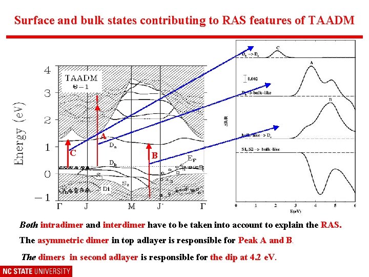
Surface and bulk states contributing to RAS features of TAADM A C B Both intradimer and interdimer have to be taken into account to explain the RAS. The asymmetric dimer in top adlayer is responsible for Peak A and B. The dimers in second adlayer is responsible for the dip at 4. 2 e. V.
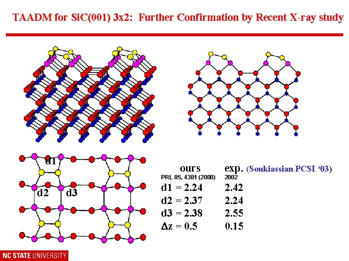
TAADM for Si. C(001) 3 x 2: Further Confirmation by Recent X-ray study d 1 d 2 ours d 3 exp. (Soukiassian PCSI ‘ 03) PRL 85, 4381 (2000) 2002 d 1 = 2. 24 d 2 = 2. 37 d 3 = 2. 38 Dz = 0. 5 2. 42 2. 24 2. 55 0. 15
![Investigate most common steps on Si(001) [Chadi, PRL 59, 1691 (1987)] Investigate most common steps on Si(001) [Chadi, PRL 59, 1691 (1987)]](http://slidetodoc.com/presentation_image_h2/8411cd59e2420acc1af2dbbbf3b1058c/image-29.jpg)
Investigate most common steps on Si(001) [Chadi, PRL 59, 1691 (1987)]
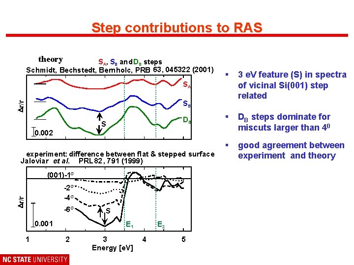
Step contributions to RAS theory SA, SB and DB steps Schmidt, Bechstedt, Bernholc, PRB 63, 045322 (2001) § 3 e. V feature (S) in spectra of vicinal Si(001) step related § DB steps dominate for miscuts larger than 40 § good agreement between experiment and theory SA Dr/r SB DB S 0. 002 experiment: difference between flat & stepped surface Jaloviar et al. PRL 82, 791 (1999) (001)-1 O Dr/r -2 O -4 O -6 O 0. 001 1 S E 1 2 3 Energy [e. V] E 2 4 5
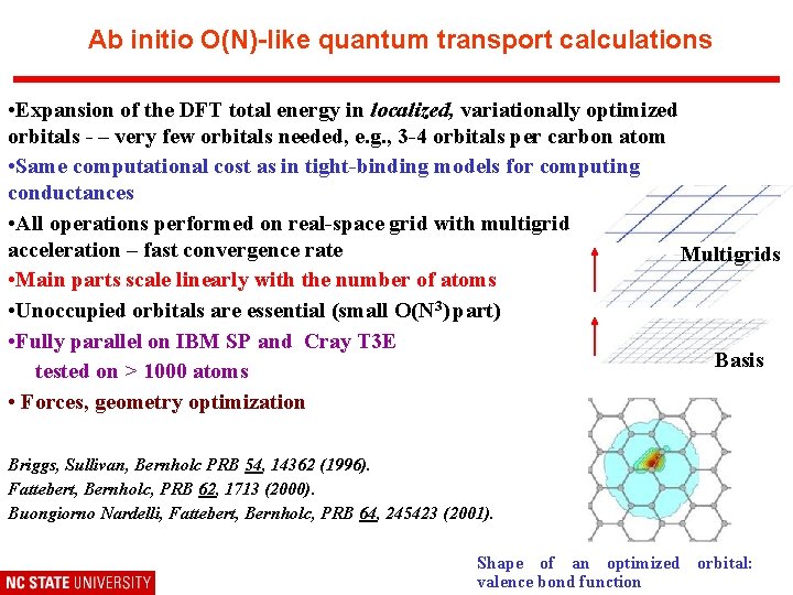
Ab initio O(N)-like quantum transport calculations • Expansion of the DFT total energy in localized, variationally optimized orbitals - – very few orbitals needed, e. g. , 3 -4 orbitals per carbon atom • Same computational cost as in tight-binding models for computing conductances • All operations performed on real-space grid with multigrid acceleration – fast convergence rate Multigrids • Main parts scale linearly with the number of atoms • Unoccupied orbitals are essential (small O(N 3) part) • Fully parallel on IBM SP and Cray T 3 E Basis tested on > 1000 atoms • Forces, geometry optimization Briggs, Sullivan, Bernholc PRB 54, 14362 (1996). Fattebert, Bernholc, PRB 62, 1713 (2000). Buongiorno Nardelli, Fattebert, Bernholc, PRB 64, 245423 (2001). Shape of an optimized orbital: valence bond function
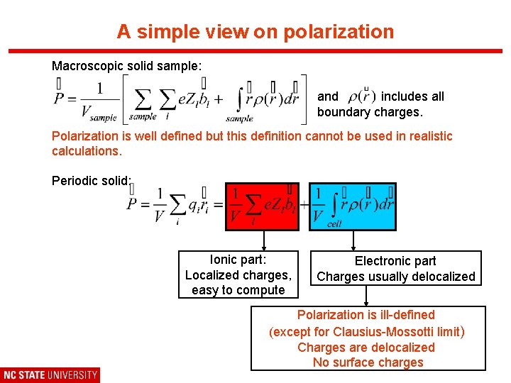
A simple view on polarization Macroscopic solid sample: and includes all boundary charges. Polarization is well defined but this definition cannot be used in realistic calculations. Periodic solid: Ionic part: Localized charges, easy to compute Electronic part Charges usually delocalized Polarization is ill-defined (except for Clausius-Mossotti limit) Charges are delocalized No surface charges
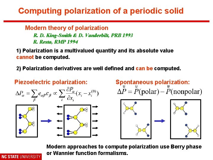
Computing polarization of a periodic solid Modern theory of polarization R. D. King-Smith & D. Vanderbilt, PRB 1993 R. Resta, RMP 1994 1) Polarization is a multivalued quantity and its absolute value cannot be computed. 2) Polarization derivatives are well defined and can be computed. Piezoelectric polarization: Spontaneous polarization: Modern approaches to compute polarization use Berry phase or Wannier function formalisms.
- Slides: 33