Atomic Scale Computational Simulation for Nanomaterials and Devices


")
 300 K Initial Temperature 300")
 Co on Al (001)")
 3 ML Co on Al(001)")

/(0001) Co on Al(111)")
 3 ML Co on Al(001)")
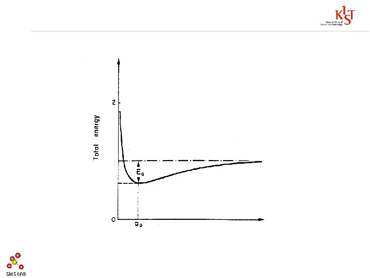
 (3) (2) (4) Reaction Coordinate")
 300 K Initial Temperature 300")
 Co 3. 5 e. V (2) (3) (4)")
 Co 3. 5")
 Co on Al (001)")


 Cu Capping layer (50Å)")
 Co (30Å) Cu buffer layer (1500Å) Si")
 Co (30Å, 5Å) Cu buffer layer (1500Å) Si")
 Co (30Å) Cu buffer layer (1500Å) Si")
 interlayer? 5Å Capping layer (50Å) 7Å Co")


- Slides: 44
Atomic Scale Computational Simulation for Nano-materials and Devices: A New Research Tool for Nanotechnology Kwang-Ryeol Lee Future Technology Research Division, KIST, Seoul, Korea 2 nd International Symposium on Bio- and Nano-Electronics in Sendai, Dec. 9 -10, 2006
Today’s Talk • Introduction to computational simulation • Role of atomic scale simulation in nanomaterials and devices research • Case Study : Asymmetry in atomic scale intermixing during deposition of thin metallic multilayers
What is Computational Simulation? Research method to investigate a complex system based on the reasonable principles of a simple system. 10 ke. V Ar on Au 75 e. V C on diamond
Molecular Dynamics Simulation Interatomic Potentials • Empirical Approach • First Principle Approach i Time evolution of Ri and vi
Hierarchy of Computer Simulation Engineering Design min Continuum Models Time ms - FEM/FDM - Monte Carlo Approach - Phase Field Theory s ns Atomic Level Simulation - Monte Carlo Approach - Classical MD ps fs Fundamental Models - First Principle Calculation - Ab initio MD 1 A 100 A Length Scale 1 m 1 mm
Computation & Simulation in Atomic Scale Ab initio Calculation Molecular Dynamic Simulation
Nanomaterials
Characteristics of Nanotechnology • Continuum media hypothesis is not allowed. ~ nm – Band Theory – Diffusion and Mechanics ~ nm
Size Dependent Properties Energy Atomic Molecules Clusters Orbitals N=2 N=10 N=1 Q-Size Particles N=2, 000 Semiconductor N>>2, 000 Vacuum Smaller Size Conduction Band hn Cd. Se Nanoparticles hn Valence Band
Scale Down Issues ~0. 1 m 1~2 nm <10 nm Kinetics based on continuum media hypothesis is not sufficient.
Chracteristics of Nanotechnology • Continuum media hypothesis is not allowed. • Large fraction of the atom lies at the surface or interface. – Abnormal Wetting – Abnormal Melting of Nano Particles – Chemical Instabilities
GMR Spin Valve Major materials issue is the interfacial structure in atomic scale
Nanoscience or Nanotechnology needs atomic scale understandings of structure, kinetics and properties.
Insufficient Experimental Tools
Methodology of Conventional R&D Synthesis & Manipulation Analysis & Characterization Modeling & Simulation
Methodology of Nanotechnology Synthesis & Manipulation Analysis & Characterization Modeling & Simulation
Computation & Simulation in Atomic Scale Ab initio Calculation Molecular Dynamic Simulation 1 nm = 1, 000 atoms 10 nm = 1, 000 atoms 100 nm = 1, 000, 000 atoms
Cluster Supercomputer & Visualization Beowulf Cluster @ CALTECH
Devices with Thin Multilayers 1~2 nm GMR Spin Valve Major materials issue is the interfacial structure in atomic scale
Thin Film Growth Model (conventional)
Calculation Methods Adatom (normal incident 0. 1 e. V) 300 K Initial Temperature 300 K Constant Temperature Fixed Atom Position • • • Co-Al EAM potential* x, y-axis : Periodic Boundary Condition z-axis : Open Surface Deposition rate: 1. 306 × 10 -1 nm/nsec MD calc. step : 0. 1 fs R. Pasianot et al, Phys. Rev. B 45, 12704 (1992). A. F. Voter et al , MRS Proc. 82, 175 (1987). C. Vailhe et al, J. Mater. Res. 12, 2559 (1997).
Deposition in Co-Al System Al on Co (001) Co on Al (001)
Asymmetry in Interfacial Intermixing 3 ML Al on Co(001) 3 ML Co on Al(001)
Radial Distribution Function of Interface Ø Co. Al compound layer of B 2 structure was formed spontaneously.
Atomic deposition behavior Al on Co(111)/(0001) Co on Al(111)
Asymmetry in Interfacial Intermixing 3 ML Al on Co(001) 3 ML Co on Al(001) • Deposition at 300 K • Initial kinetic energy 0. 1 e. V
Activation Barrier for Intermixing (1) (3) (2) (4) Reaction Coordinate
Calculation Methods Adatom (normal incident 0. 1 e. V) 300 K Initial Temperature 300 K Constant Temperature Fixed Atom Position • • • Co-Al EAM potential* x, y-axis : Periodic Boundary Condition z-axis : Open Surface Deposition rate: 1. 306 × 10 -1 nm/nsec MD calc. step : 0. 1 fs R. Pasianot et al, Phys. Rev. B 45, 12704 (1992). A. F. Voter et al , MRS Proc. 82, 175 (1987). C. Vailhe et al, J. Mater. Res. 12, 2559 (1997).
Acceleration of Adatoms near Surface (1) Co 3. 5 e. V (2) (3) (4) Al (1) (3) (2) (4)
Kinetic Criteria for Intermixing Activation Barrier for Mixing Local Acceleration (1) Co 3. 5 e. V Al (2) (1) (3) Reaction Coordinate (3) (4) (2) (4)
Deposition in Co-Al System Al on Co (001) Co on Al (001)
Asymmetry of Surface Reaction Al on Co Co on Al Do you have experimental evidence?
Magnetic Properties of Co-Al system Spin-Up FCC - Al B 2 - Co. Al Spin-Down Spin resolved DOS HCP - Co
Magnetic properties of Co-Al Thin Layer MOKE (Magneto-Optic Kerr effects) Cu Capping layer (50Å) Co (30Å) Al (30Å) Cu buffer layer (1500Å) Co (30Å) Cu Capping layer (50Å) Co (30Å) Al (840Å) Cu buffer layer (1500Å) Si substrate
Effect of Coating Sequence Capping layer (50Å) Co (30Å) Cu buffer layer (1500Å) Si substrate Al Capping layer (50Å) Al (30Å) Co (30Å) Cu buffer layer (1500Å) Co Al. Si substrate Capping layer (50Å) Co (30Å) Al (840Å) Si substrate
Co Thickness Effect Capping layer (50Å) Co (30Å, 5Å) Cu buffer layer (1500Å) Si substrate
Effect of Coating Sequence Capping layer (50Å) Co (30Å) Cu buffer layer (1500Å) Si substrate Al Capping layer (50Å) Al (30Å) Co (30Å) Cu buffer layer (1500Å) Co Al. Si substrate Capping layer (50Å) Co (30Å) Al (840Å) Si substrate
How thick is the nonmagnetic (B 2) interlayer? 5Å Capping layer (50Å) 7Å Co (variable thickness) Al (840Å) Si substrate 10Å 30Å
Thickness of B 2 Layer : 3 ML ~ 10Å
Summary Al on Co Co on Al Asymmetry in interfacial intermixing was observed in both MD simulation and experiment.
Acknowledgement • Financial Support – Core Capability Enhancement Program of KIST (V 00910, E 19190) • Collaborators – KIST • Mr. Sang-Pil Kim • Dr. Seung-Cheol Lee – Hanyang University • Prof. Yong-Jae Chung – Yonsei University • Prof. Chungnam Whang • Dr. Jae Young Park • Ms. Hyunmi Hwang
Computational Materials Simulation Lab. http: //diamond. kist. re. kr/SMS