Atomic Force Microscopy Studies of Gold Thin Films
- Slides: 21

Atomic Force Microscopy Studies of Gold Thin Films Dara Gough Advisor: Prof. King School of Materials Engineering Thin Films and Interfaces

Overview • • Brief Background Purpose of the project Project objectives Why use gold films? Experimental approach Setbacks Results School of Materials Engineering Thin Films and Interfaces

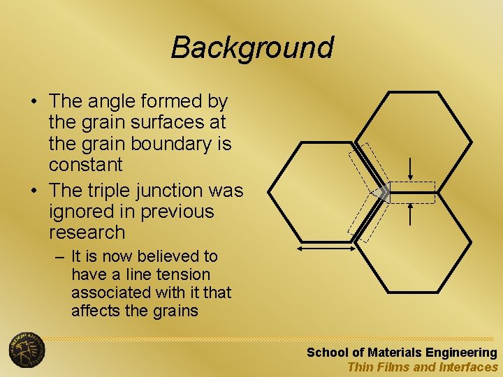
Background • The angle formed by the grain surfaces at the grain boundary is constant • The triple junction was ignored in previous research – It is now believed to have a line tension associated with it that affects the grains School of Materials Engineering Thin Films and Interfaces

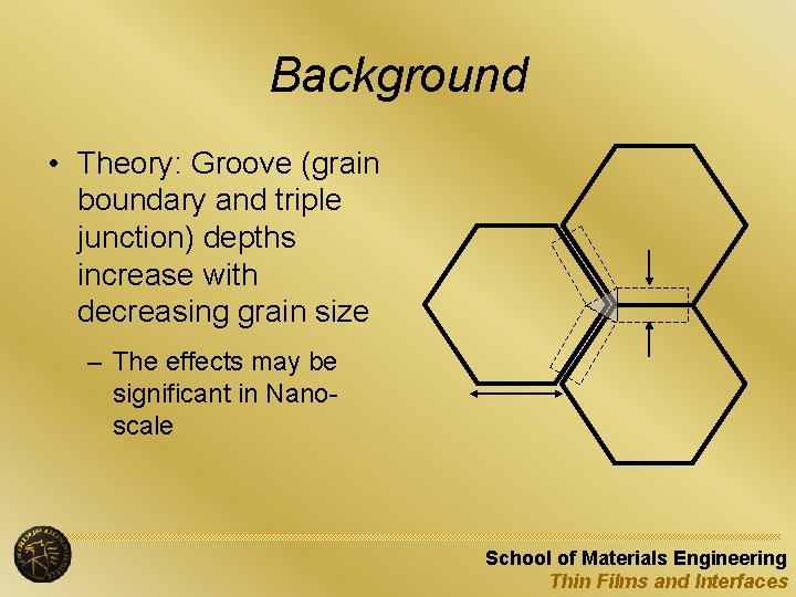
Background • Theory: Groove (grain boundary and triple junction) depths increase with decreasing grain size – The effects may be significant in Nanoscale School of Materials Engineering Thin Films and Interfaces

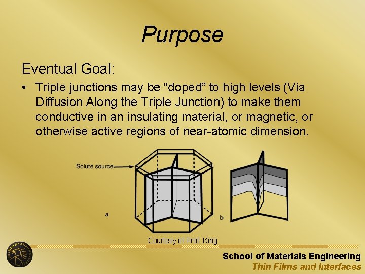
Purpose Eventual Goal: • Triple junctions may be “doped” to high levels (Via Diffusion Along the Triple Junction) to make them conductive in an insulating material, or magnetic, or otherwise active regions of near-atomic dimension. Courtesy of Prof. King School of Materials Engineering Thin Films and Interfaces

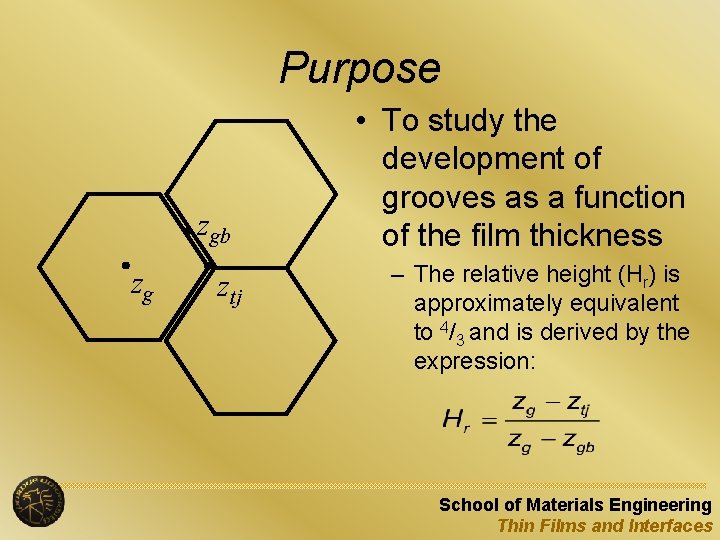
Purpose zgb zg ztj • To study the development of grooves as a function of the film thickness – The relative height (Hr) is approximately equivalent to 4/3 and is derived by the expression: School of Materials Engineering Thin Films and Interfaces

Objectives • To create gold thin films of varying thicknesses • To anneal the film samples • To obtain surface profiles of the samples School of Materials Engineering Thin Films and Interfaces

Objectives • To analyze the surface profiles and obtain data points – The data points are the height differences between: • The center of the grain and the middle of the grain boundary • The center of the grain and the triple junction School of Materials Engineering Thin Films and Interfaces

Why Gold? • Gold is the ideal metal for this experiment because: – It is polycrystalline – It does not oxidize in atmospheric conditions – It evaporates easily in high temperature-low pressure environment School of Materials Engineering Thin Films and Interfaces

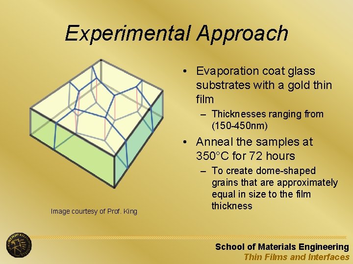
Experimental Approach • Evaporation coat glass substrates with a gold thin film – Thicknesses ranging from (150 -450 nm) • Anneal the samples at 350°C for 72 hours Image courtesy of Prof. King – To create dome-shaped grains that are approximately equal in size to the film thickness School of Materials Engineering Thin Films and Interfaces

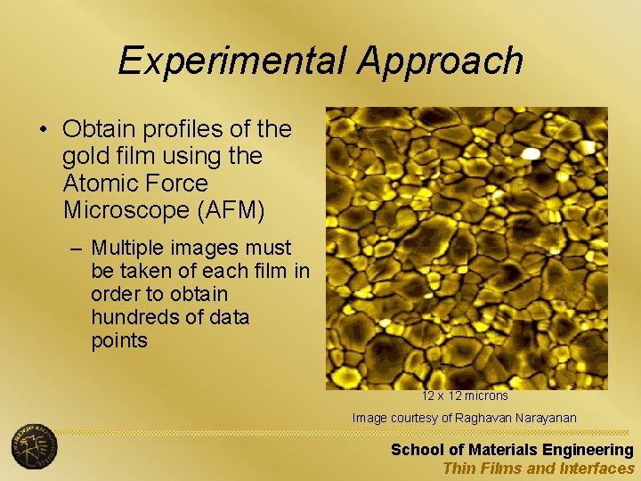
Experimental Approach • Obtain profiles of the gold film using the Atomic Force Microscope (AFM) – Multiple images must be taken of each film in order to obtain hundreds of data points 12 x 12 microns Image courtesy of Raghavan Narayanan School of Materials Engineering Thin Films and Interfaces

Experimental Approach • The next step in the project is to analyze the images – This is done using Scanning Probe Microscopy Software – The software analyzes changes in height along the surface and provides relative height differences School of Materials Engineering Thin Films and Interfaces

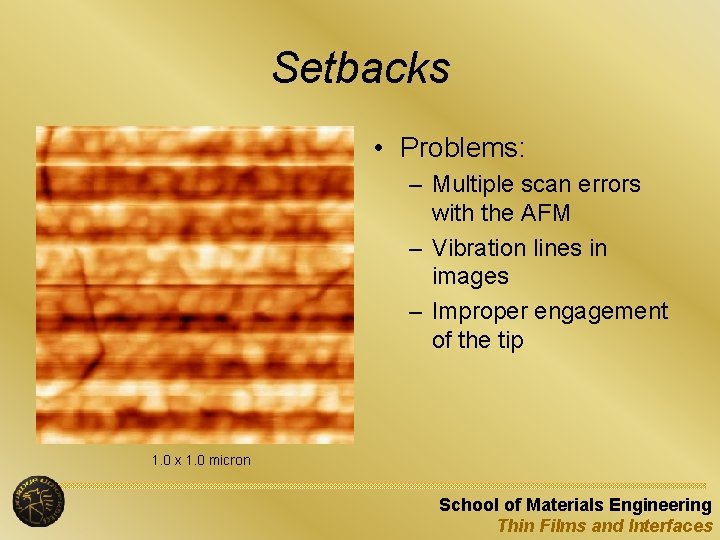
Setbacks • Problems: – Multiple scan errors with the AFM – Vibration lines in images – Improper engagement of the tip 1. 0 x 1. 0 micron School of Materials Engineering Thin Films and Interfaces

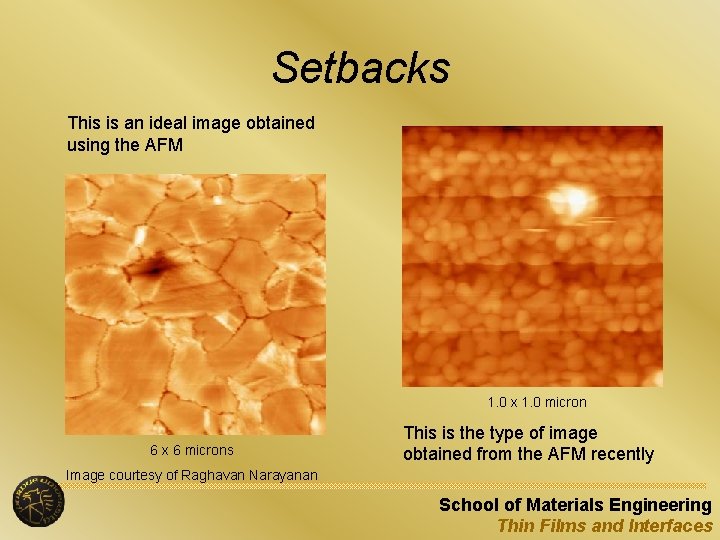
Setbacks This is an ideal image obtained using the AFM 1. 0 x 1. 0 micron 6 x 6 microns This is the type of image obtained from the AFM recently Image courtesy of Raghavan Narayanan School of Materials Engineering Thin Films and Interfaces

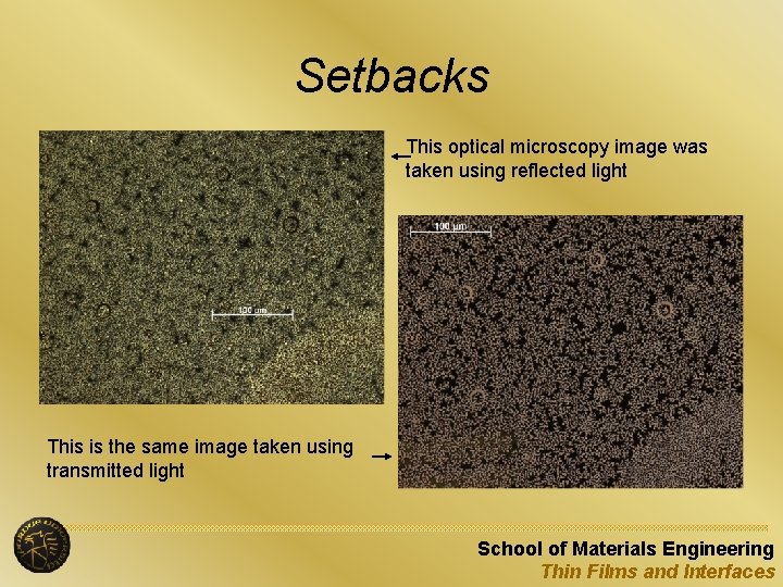
Setbacks • My initial set of gold films was overannealed – This resulted in the gold receding from the substrate School of Materials Engineering Thin Films and Interfaces

Setbacks This optical microscopy image was taken using reflected light This is the same image taken using transmitted light School of Materials Engineering Thin Films and Interfaces

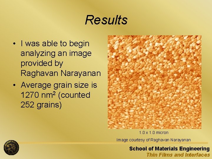
Results • I was able to begin analyzing an image provided by Raghavan Narayanan • Average grain size is 1270 nm 2 (counted 252 grains) 1. 0 x 1. 0 micron Image courtesy of Raghavan Narayanan School of Materials Engineering Thin Films and Interfaces

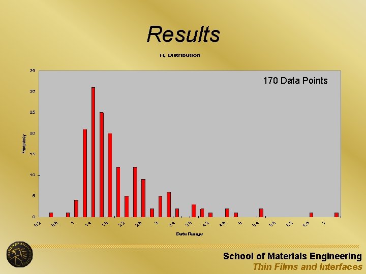
Results 170 Data Points School of Materials Engineering Thin Films and Interfaces

Future Work • Take more surface profiles using the AFM – Over a wider variety of film thicknesses (grain sizes) • Analyze the surface profiles using the Scanning Probe Microscopy Software School of Materials Engineering Thin Films and Interfaces

Acknowledgements • I would like to thank the National Science Foundation (REU Grant DMR-0243830) for financing my research alongside the Department of Energy • I would like to thank Prof. Alex King for his support and guidance • I would also like to thank Raghavan Narayanan for his assistance throughout the course of the project School of Materials Engineering Thin Films and Interfaces

Questions? (Questions) School of Materials Engineering Thin Films and Interfaces