ATLAS Evaluation of Si Ge bi CMOS Technologies
ATLAS Evaluation of Si. Ge bi. CMOS Technologies for Next Generation Strip Readout ATLAS Tracker Upgrade Workshop Genova 19 -Jul-2005 A. A. Grillo SCIPP – UCSC 19 -Jul-2005 1 Si. Ge bi. CMOS for Next Gen Strip Readout A. A. Grillo SCIPP-UCSC 1
Participants ATLAS D. E. Dorfan, A. A. Grillo, J. Metcalfe, M Rogers, H. F. -W. Sadrozinski, A. Seiden, E. Spencer, M. Wilder SCIPP-UCSC Collaborators: A. Sutton, J. D. Cressler Georgia Tech, Atlanta, GA 30332 -0250, USA M. Ullan, M. Lozano CNM, Barcelona 19 -Jul-2005 2 Si. Ge bi. CMOS for Next Gen Strip Readout A. A. Grillo SCIPP-UCSC 2
Bipolar for Large C – Fast ts ATLAS We have shown for past experiments that the bipolar technology has advantages over CMOS in power and performance for frontend amplification of silicon strip readout when the capacitive loads are high and the shaping times short. • • • ZEUS-LPS SSC-SDC ATLAS-SCT Tek-Z IC LBIC IC ABCD, CAFE-M, CAFE-P ICs Since CMOS is the preferred technology for back-end data processing, bi. CMOS technologies have not been readily available, making it difficult to find a one chip solution. Experience with the commercial 0. 25 mm CMOS has shown the great advantage of using a high volume commercial rather than a niche technology. 19 -Jul-2005 3 Si. Ge bi. CMOS for Next Gen Strip Readout A. A. Grillo SCIPP-UCSC 3
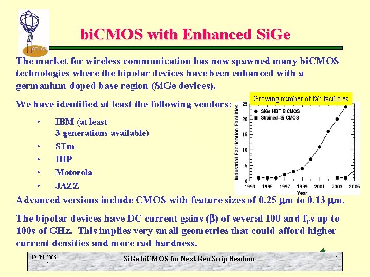
bi. CMOS with Enhanced Si. Ge ATLAS The market for wireless communication has now spawned many bi. CMOS technologies where the bipolar devices have been enhanced with a germanium doped base region (Si. Ge devices). We have identified at least the following vendors: • • • Growing number of fab facilities IBM (at least 3 generations available) STm IHP Motorola JAZZ Advanced versions include CMOS with feature sizes of 0. 25 mm to 0. 13 mm. The bipolar devices have DC current gains (b) of several 100 and f. Ts up to 100 s of GHz. This implies very small geometries that could afford higher current densities and more rad-hardness. 19 -Jul-2005 4 Si. Ge bi. CMOS for Next Gen Strip Readout A. A. Grillo SCIPP-UCSC 4
Tracker Regions Amenable for Si. Ge ATLAS For the inner tracker layers, pixel detectors will be needed, and their small capacitances allow the use of deep sub-micron CMOS as an efficient readout technology. Starting at a radius of about 20 cm, at fluence levels of 1015 n/cm 2, short strips can be used, with a detector length of about 3 cm and capacitances of the order of 5 p. F. At a radius of about 60 cm, the expected fluence is a few times 1014 p/cm 2, and longer strips of about 10 cm and capacitance of 15 p. F can be used. It is in these two outer regions with sensors with larger capacitive loads where bipolar Si. Ge might be used in the front-end readout ASICs with welcome power savings while still maintaining fast shaping times. 19 -Jul-2005 5 Si. Ge bi. CMOS for Next Gen Strip Readout A. A. Grillo SCIPP-UCSC 5

Biasing the Analogue Circuit ATLAS The analog section of a readout IC for silicon strips typically has a special front transistor, selected to minimize noise (often requiring a larger current than the other transistors), and a large number of additional transistors used in the shaping sections and for signal-level discrimination. The current for the front transistor is selected in order to achieve the desired transconductance (minimize noise). For the other bipolar devices, bias levels for the other transistors are determined to achieve the necessary rad-hardness, matching and shaping times. Depending upon the performance (especially radiation hardness) of the bipolar process, power savings could be realized in both the front transistor and in the other parts of the analogue circuit. 19 -Jul-2005 6 Si. Ge bi. CMOS for Next Gen Strip Readout A. A. Grillo SCIPP-UCSC 6
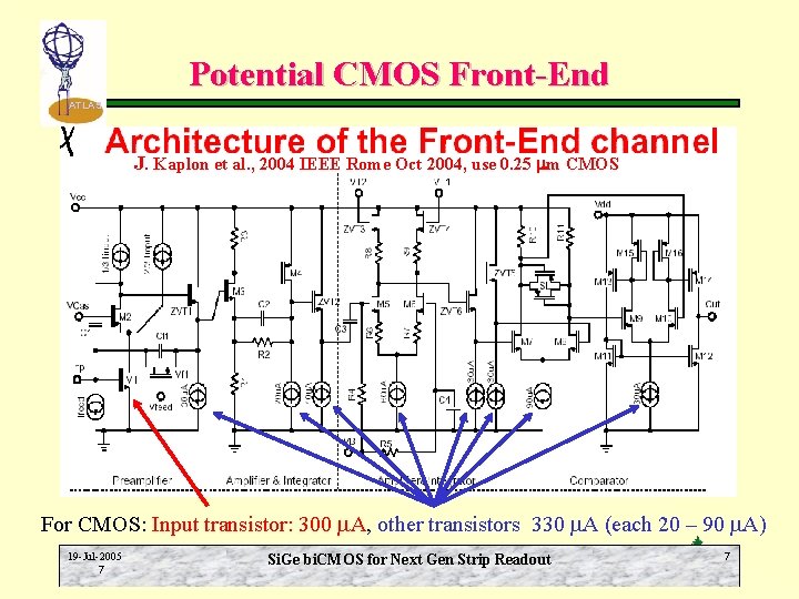
Potential CMOS Front-End ATLAS J. Kaplon et al. , 2004 IEEE Rome Oct 2004, use 0. 25 mm CMOS For CMOS: Input transistor: 300 m. A, other transistors 330 m. A (each 20 – 90 m. A) 19 -Jul-2005 7 Si. Ge bi. CMOS for Next Gen Strip Readout A. A. Grillo SCIPP-UCSC 7
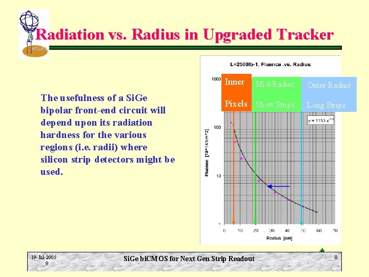
Radiation vs. Radius in Upgraded Tracker ATLAS Inner The usefulness of a Si. Ge bipolar front-end circuit will depend upon its radiation hardness for the various regions (i. e. radii) where silicon strip detectors might be used. 19 -Jul-2005 8 Mid-Radius Pixels Short Strips Si. Ge bi. CMOS for Next Gen Strip Readout Outer Radius Long Strips A. A. Grillo SCIPP-UCSC 8
First Attempts at Radiation Testing ATLAS Radiation testing has been performed on some Si. Ge devices by our Georgia Tech collaborators up to a fluence of 1 x 10¹⁴ p/cm 2 and they have demonstrated acceptable performance. (See for example: http: //isde. vanderbilt. edu/Content/muri/2005 MURI/Cressler_MURI. ppt) In order to extend this data to higher fluences, we obtained some arrays of test structures from our collaborator at Georgia Tech. These were from a b-enhanced 5 HP process from IBM. (i. e. the b was closer to that of the IBM 7 HP process. ) The parts were tested at UCSC and with the help of RD 50 collaborators (Michael Moll & Maurice Glaser) they were irradiated in Fall 2004 at the CERN PS and then re-tested at UCSC. For expediency, all terminals were grounded during the irradiation (slightly worse than with normal biasing). Annealing was performed after initial post-rad testing. 19 -Jul-2005 9 Si. Ge bi. CMOS for Next Gen Strip Readout A. A. Grillo SCIPP-UCSC 9
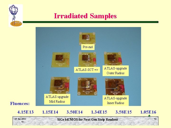
Irradiated Samples ATLAS Pre-rad ATLAS-SCT => Fluences: 4. 15 E 13 19 -Jul-2005 10 ATLAS-upgrade Mid Radius 1. 15 E 14 3. 50 E 14 ATLAS-upgrade Outer Radius ATLAS-upgrade Inner Radius 1. 34 E 15 3. 58 E 15 Si. Ge bi. CMOS for Next Gen Strip Readout 1. 05 E 16 A. A. Grillo SCIPP-UCSC 10
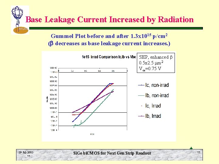
Base Leakage Current Increased by Radiation ATLAS Gummel Plot before and after 1. 3 x 10¹⁵ p/cm 2 (b decreases as base leakage current increases. ) 5 HP, enhanced b 0. 5 x 2. 5 mm 2 Vce=0. 75 V 19 -Jul-2005 11 Si. Ge bi. CMOS for Next Gen Strip Readout A. A. Grillo SCIPP-UCSC 11
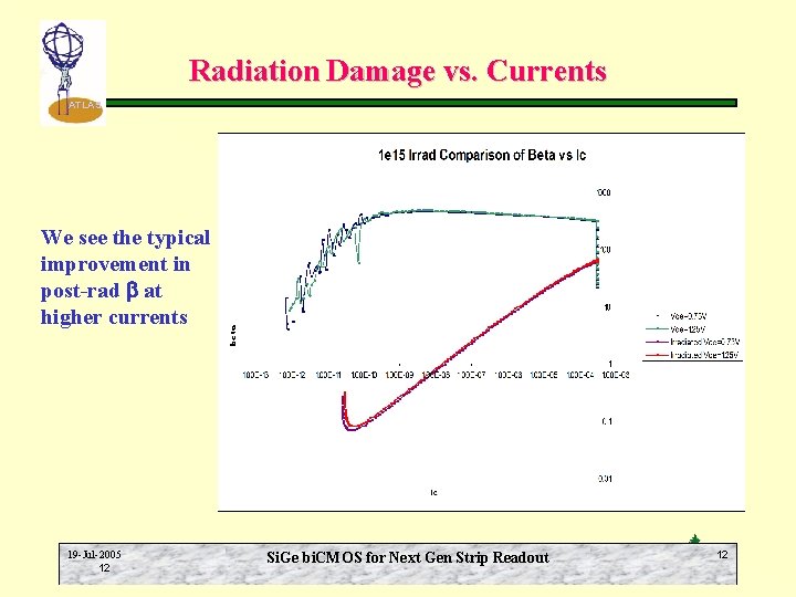
Radiation Damage vs. Currents ATLAS We see the typical improvement in post-rad b at higher currents 19 -Jul-2005 12 Si. Ge bi. CMOS for Next Gen Strip Readout A. A. Grillo SCIPP-UCSC 12
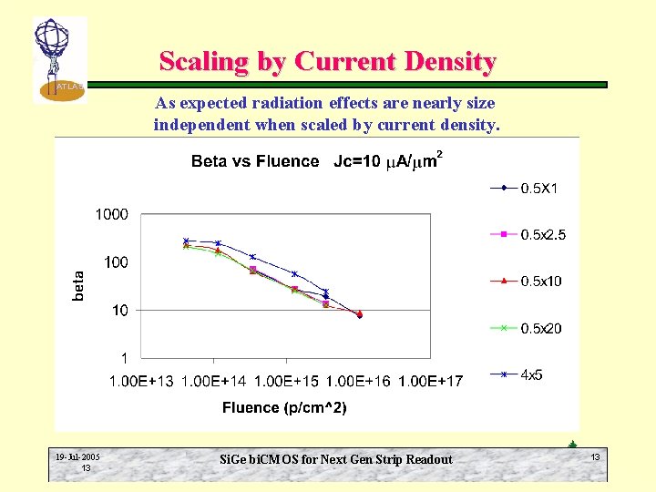
Scaling by Current Density ATLAS As expected radiation effects are nearly size independent when scaled by current density. 19 -Jul-2005 13 Si. Ge bi. CMOS for Next Gen Strip Readout A. A. Grillo SCIPP-UCSC 13
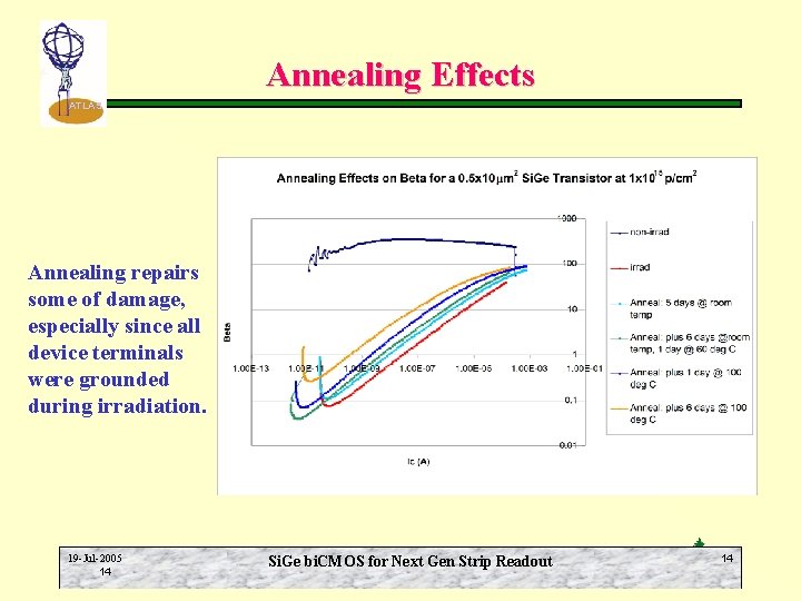
Annealing Effects ATLAS Annealing repairs some of damage, especially since all device terminals were grounded during irradiation. 19 -Jul-2005 14 Si. Ge bi. CMOS for Next Gen Strip Readout A. A. Grillo SCIPP-UCSC 14
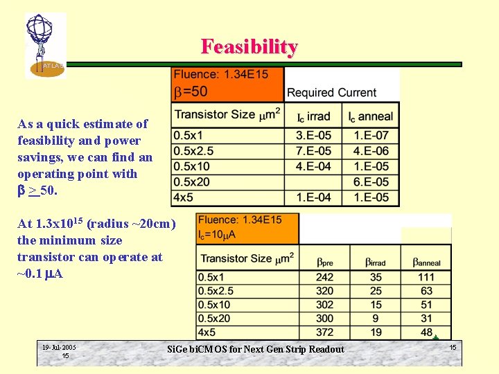
Feasibility ATLAS As a quick estimate of feasibility and power savings, we can find an operating point with b > 50. At 1. 3 x 10¹⁵ (radius ~20 cm) the minimum size transistor can operate at ~0. 1 m. A 19 -Jul-2005 15 Si. Ge bi. CMOS for Next Gen Strip Readout A. A. Grillo SCIPP-UCSC 15

First Guess at Potential Power Savings ATLAS Using similar estimates of bias settings and transistor counts, a crude estimate for power can be obtained. A full design and simulation are still needed. CHIP TECHNOLOGY FEATURE 0. 25 mm CMOS ABCDS/FE J. Kaplon et al. , (IEEE Rome Oct 2004) 330 m. A 0. 8 m. W Power: Bias for all but front transistor IBM enhanced 5 HP Si. Ge 8*5 m. A = 40 m. A 0. 1 m. W (conservative) Power: Front bias for 25 p. F load 300 m. A 0. 75 m. W 150 m. A 0. 375 m. W Power: Front bias for 7 p. F load 120 m. A 0. 3 m. W 50 m. A 0. 13 m. W Total Power (7 p. F) Total Power (25 p. F) 19 -Jul-2005 16 2 x 10¹⁵ 3 x 10¹⁴ 1. 1 m. W 0. 23 m. W 1. 5 m. W 0. 48 m. W Si. Ge bi. CMOS for Next Gen Strip Readout A. A. Grillo SCIPP-UCSC 16

Conclusions ATLAS First tests of one Si. Ge bi. CMOS process indicate that the bipolar devices may be sufficiently rad-hard for the upgraded ATLAS tracker, certainly in the outer-radius region and even perhaps in the mid-radius region. A crude estimate of power consumption for such a Si. Ge front-end circuit indicates that significant power savings might be achieved. More work is needed to both confirm the radiation hardness and arrive at more accurate estimates of power savings. In particular, with so many potential commercial vendors available, it is important to understand if the post-radiation performance is generic to the Si. Ge technology or if it is specific to some versions. 19 -Jul-2005 17 Si. Ge bi. CMOS for Next Gen Strip Readout A. A. Grillo SCIPP-UCSC 17
Work Ahead ATLAS Along with our collaborators, we plan two parallel paths of work. First, we plan more irradiations with several Si. Ge processes. In particular, we plan to test at least the IBM 5 HP, IBM enhanced 5 HP, IBM 8 HP, IHP SG 25 H 2 and one from STm. • • • CNM has obtained a first set of test structures from IHP and is proceeding. UCSC expects to receive the IBM test structures this summer. We have been promised test structures from STm but a schedule is not yet fixed. To obtain a better handle on the true power savings, we will pick one of the available processes and design a prototype front-end circuit. This will be fabricated to further test the subtleties of the process. 19 -Jul-2005 18 Si. Ge bi. CMOS for Next Gen Strip Readout A. A. Grillo SCIPP-UCSC 18
- Slides: 18