ASYNCHRONOUS CIRCUITS A GENERAL MODEL OF A SEQUENTIAL



- Slides: 35

ASYNCHRONOUS CIRCUITS

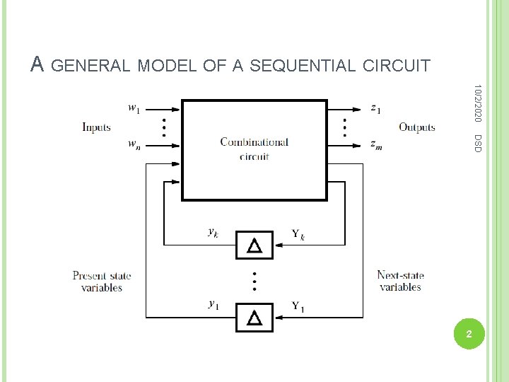
A GENERAL MODEL OF A SEQUENTIAL CIRCUIT 10/2/2020 DSD 2

10/2/2020 Asynchronous sequential Synchronous sequential DSD 3

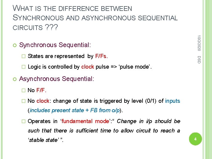
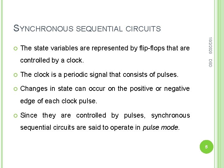
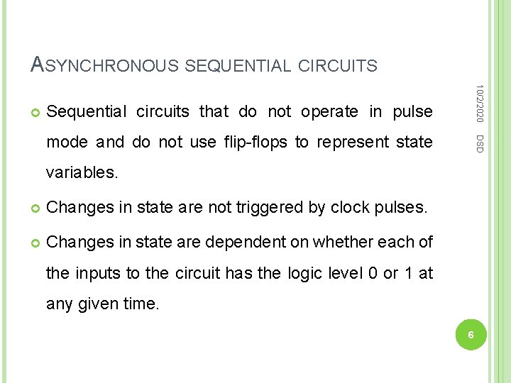
WHAT IS THE DIFFERENCE BETWEEN SYNCHRONOUS AND ASYNCHRONOUS SEQUENTIAL CIRCUITS ? ? ? Synchronous Sequential: � States are represented by F/Fs. � Logic is controlled by clock pulse => ‘pulse mode’. DSD 10/2/2020 Asynchronous Sequential: � No F/F. � No clock: change of state is triggered by level (0/1) of inputs (includes present state + FB from o/p). � Operates in ‘fundamental mode’: “ Change in i/p should be such that there is sufficient time to allow circuit to reach a ‘stable state’ ”. 4

SYNCHRONOUS SEQUENTIAL CIRCUITS 10/2/2020 The state variables are represented by flip-flops that are The clock is a periodic signal that consists of pulses. Changes in state can occur on the positive or negative DSD controlled by a clock. edge of each clock pulse. Since they are controlled by pulses, synchronous sequential circuits are said to operate in pulse mode. 5

ASYNCHRONOUS SEQUENTIAL CIRCUITS 10/2/2020 Sequential circuits that do not operate in pulse DSD mode and do not use flip-flops to represent state variables. Changes in state are not triggered by clock pulses. Changes in state are dependent on whether each of the inputs to the circuit has the logic level 0 or 1 at any given time. 6

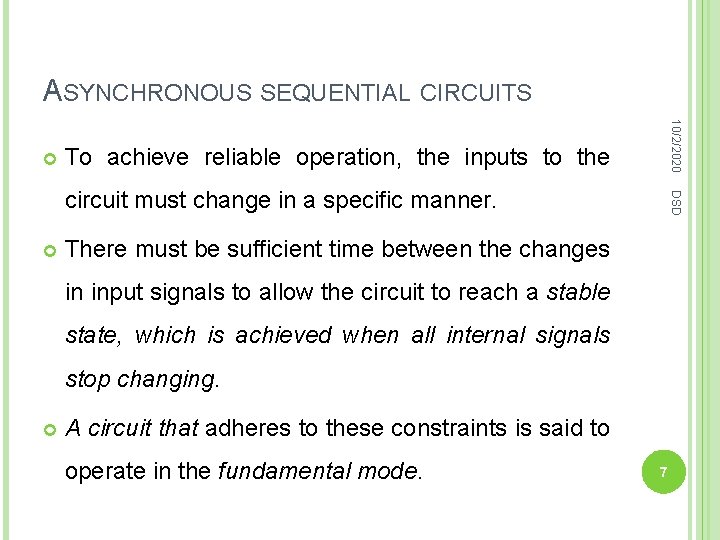
ASYNCHRONOUS SEQUENTIAL CIRCUITS 10/2/2020 To achieve reliable operation, the inputs to the DSD circuit must change in a specific manner. There must be sufficient time between the changes in input signals to allow the circuit to reach a stable state, which is achieved when all internal signals stop changing. A circuit that adheres to these constraints is said to operate in the fundamental mode. 7

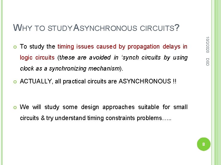
WHY TO STUDY ASYNCHRONOUS CIRCUITS? 10/2/2020 To study the timing issues caused by propagation delays in DSD logic circuits (these are avoided in ‘synch circuits by using clock as a synchronizing mechanism). ACTUALLY, all practical circuits are ASYNCHRONOUS !! We will study some design approaches suitable for small circuits & try understand timing constraints problems…. . 8

ASYNCHRONOUS CIRCUITS: BASIC REQUIREMENTS Inputs do NOT change SIMULTANEOUSLY DSD No clock for synchronizing. 10/2/2020 9

10/2/2020 DSD ASYNCHRONOUS BEHAVIOR 10

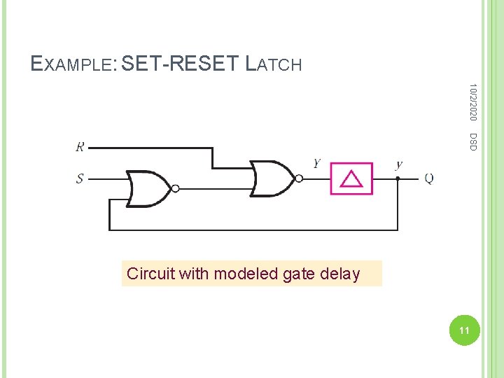
EXAMPLE: SET-RESET LATCH 10/2/2020 DSD Circuit with modeled gate delay 11

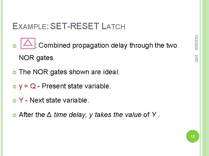
EXAMPLE: SET-RESET LATCH : Combined propagation delay through the two The NOR gates shown are ideal. y = Q - Present state variable. Y - Next state variable. After the Δ time delay, y takes the value of Y. DSD NOR gates. 10/2/2020 12

10/2/2020 DSD ANALYSIS 13

THE ANALYSIS PROCESS - STEPS INVOLVED Each FB path is cut (only one cut per loop) & a 2. � I/P to each delay element = NS variable ‘Y’. � O/P of each delay element = PS variable ‘y’. � Minimal no. of cuts to be made - called ‘cut set’. DSD delay element inserted at that point: 10/2/2020 1. Derive expressions for NS & O/P from the circuit. 14

THE ANALYSIS PROCESS - STEPS INVOLVED Derive excitation table corresponding to NS & 4. DSD O/P expressions. 10/2/2020 3. Obtain ‘flow table’ (associate arbitrary names like S 1, S 2… )with encoded states. 5. Derive state diagram from the flow table. 15

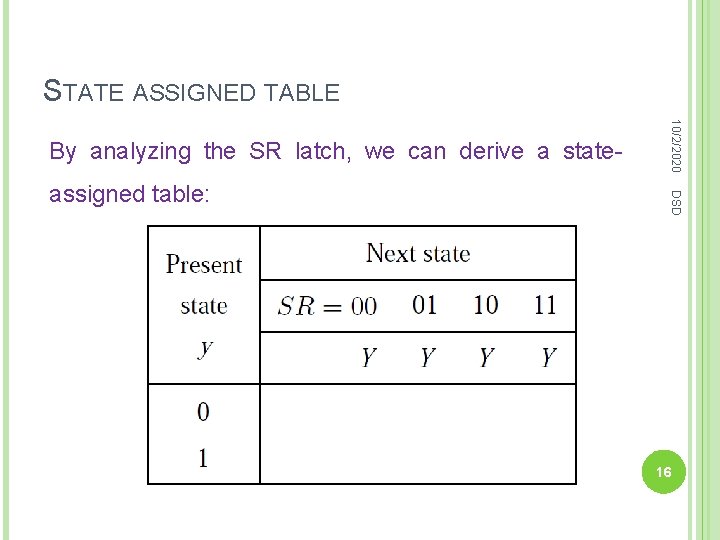
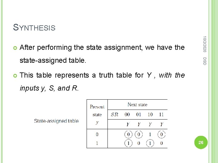
STATE ASSIGNED TABLE DSD assigned table: 10/2/2020 By analyzing the SR latch, we can derive a state- 16

ANALYSIS: HOW THE CIRCUIT BEHAVES. When y = Y , the state of the circuit will not change. DSD We say that the circuit is stable under such 10/2/2020 conditions. When ever an input causes the condition y /= Y , the circuit is not stable. After the time delay, the circuit changes to the new present state. 17

ANALYSIS: HOW THE CIRCUIT BEHAVES. 10/2/2020 DSD Discuss in details for each combination of SR when y = 0 and y = 1 how state changes – Refer “Fundamentals of digital logic with VHDL design” by Stephen Brown. 18

10/2/2020 DSD FSM MODEL FOR THE SR LATCH 19

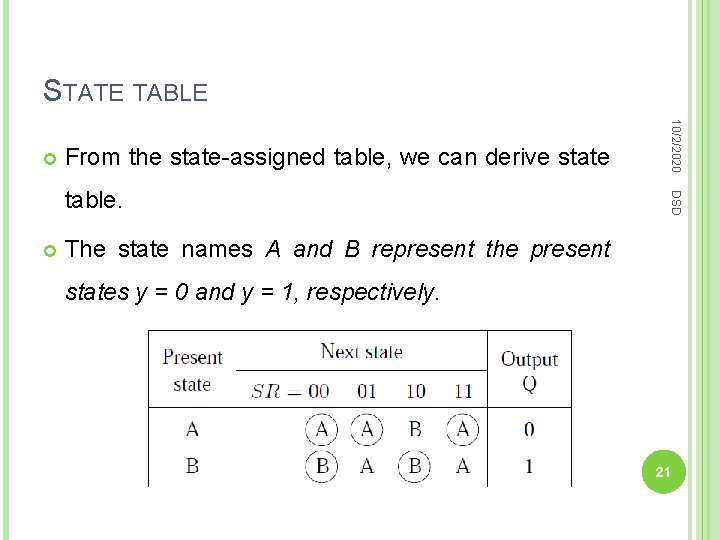
STATE TABLE The concept of stable states is very important in the DSD context of asynchronous sequential circuits. 10/2/2020 For a given valuation of inputs, if a circuit reaches a particular state and remains in this state, then the state is said to be stable. To clearly indicate the conditions under which the circuit is stable, it is customary to encircle the stable states in the table 20

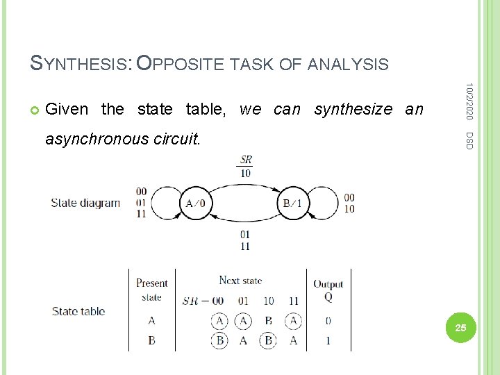
STATE TABLE From the state-assigned table, we can derive state DSD table. 10/2/2020 The state names A and B represent the present states y = 0 and y = 1, respectively. 21

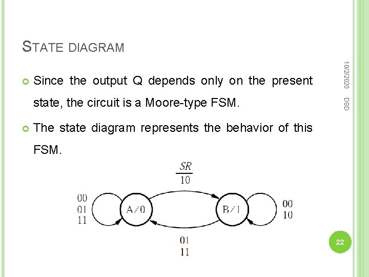
STATE DIAGRAM Since the output Q depends only on the present DSD state, the circuit is a Moore-type FSM. 10/2/2020 The state diagram represents the behavior of this FSM. 22

10/2/2020 DSD SYNTHESIS 23

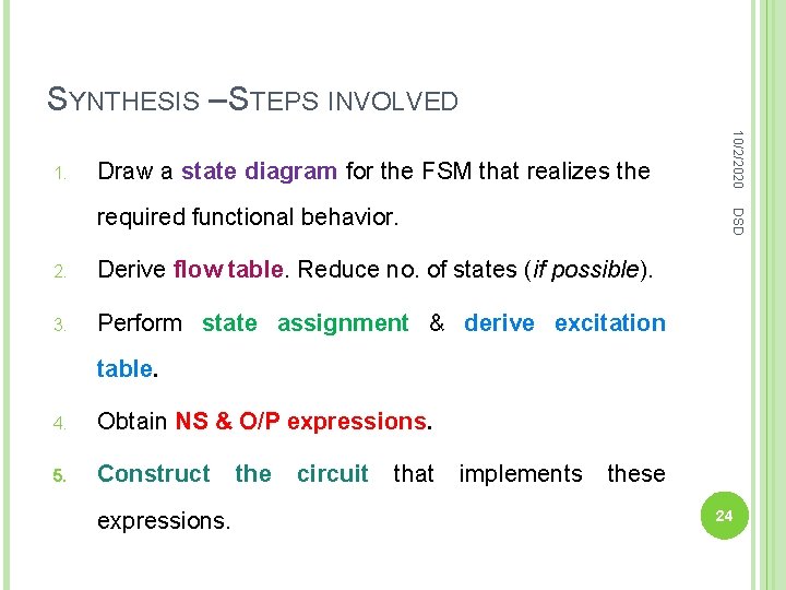
SYNTHESIS – STEPS INVOLVED Draw a state diagram for the FSM that realizes the DSD required functional behavior. 10/2/2020 1. 2. Derive flow table. Reduce no. of states (if possible). 3. Perform state assignment & derive excitation table. 4. Obtain NS & O/P expressions. 5. Construct expressions. the circuit that implements these 24

SYNTHESIS: OPPOSITE TASK OF ANALYSIS Given the state table, we can synthesize an DSD asynchronous circuit. 10/2/2020 25

SYNTHESIS After performing the state assignment, we have the DSD state-assigned table. 10/2/2020 This table represents a truth table for Y , with the inputs y, S, and R. 26

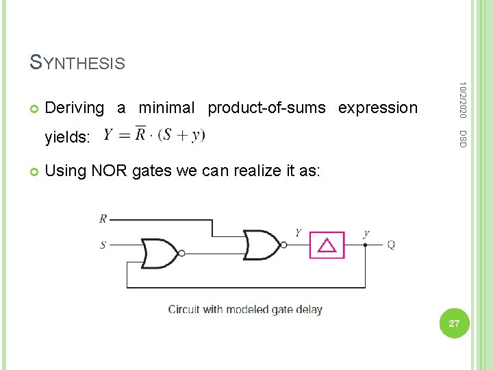
SYNTHESIS Deriving a minimal product-of-sums expression DSD yields: 10/2/2020 Using NOR gates we can realize it as: 27

10/2/2020 DSD ANALYSIS OF MEALY MODEL 28

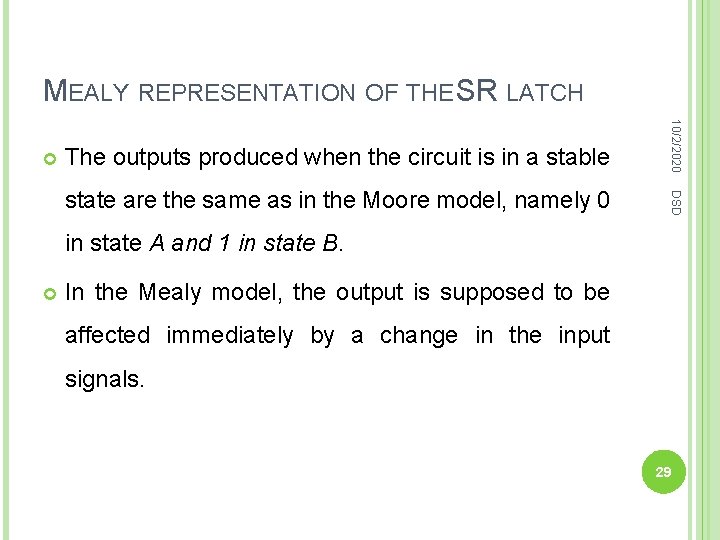
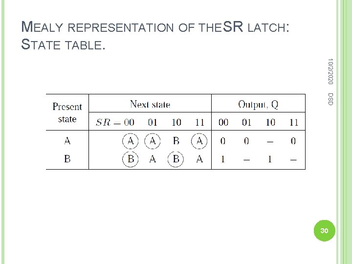
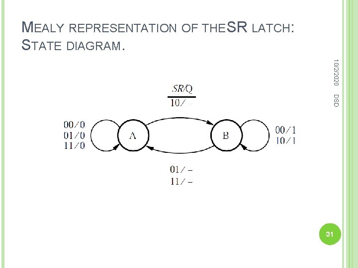
MEALY REPRESENTATION OF THE SR LATCH The outputs produced when the circuit is in a stable DSD state are the same as in the Moore model, namely 0 10/2/2020 in state A and 1 in state B. In the Mealy model, the output is supposed to be affected immediately by a change in the input signals. 29

MEALY REPRESENTATION OF THE SR LATCH: STATE TABLE. 10/2/2020 DSD 30

MEALY REPRESENTATION OF THE SR LATCH: STATE DIAGRAM. 10/2/2020 DSD 31

MEALY REPRESENTATION OF THE SR LATCH. The entry is kept un specified when there is a DSD change of state because we cannot gain anything 10/2/2020 more if the output value is changed a little sooner. Anyway the out put will change the value when it achieves the next state. Leaving the entry unspecified allows us to assign either 0 or 1 to it, which may make the circuit that implements the state table somewhat simpler. 32

10/2/2020 DSD TERMINOLOGY 33

TERMINOLOGY IN ASYNCHRONOUS SEQUENTIAL CIRCUIT DESIGN Instead of a “state table, ” it is more common to speak of DSD a flow table, which indicates how the changes in state 10/2/2020 flow as a result of the changes in the input signals. Instead of a “state-assigned table, ” it is usual to refer to a transition table or an excitation table. A flow table will define the state changes and outputs that must be generated. An excitation table will depict the transitions in terms of the state variables. 34

10/2/2020 DSD THANK YOU 35