Asynchronous and Synchronous Serial Communication COE 306 Introduction
![LPC 176 x/5 x UART Registers v The UARTn RLS interrupt (Un. IIR[3: 1] LPC 176 x/5 x UART Registers v The UARTn RLS interrupt (Un. IIR[3: 1]](https://slidetodoc.com/presentation_image_h/ce8e085b4b9e5442b3ce9c406af3e9c1/image-102.jpg)
- Slides: 113

Asynchronous and Synchronous Serial Communication COE 306: Introduction to Embedded Systems Dr. Aiman El-Maleh Computer Engineering Department College of Computer Sciences and Engineering King Fahd University of Petroleum and Minerals

Next. . . v Types of Data Transmission v Serial Transmission v Synchronous vs. Asynchronous Transmission v Serial Peripheral Interface (SPI) v Inter Integrated Circuit (I 2 C) v Universal Asynchronous Receiver Transmitter (UART) Asynchronous and Synchronous Serial Communication slide 2 COE 306– Introduction to Embedded System– KFUPM

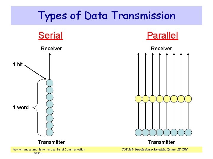
Types of Data Transmission Serial Parallel Receiver Transmitter 1 bit 1 word Asynchronous and Synchronous Serial Communication slide 3 COE 306– Introduction to Embedded System– KFUPM

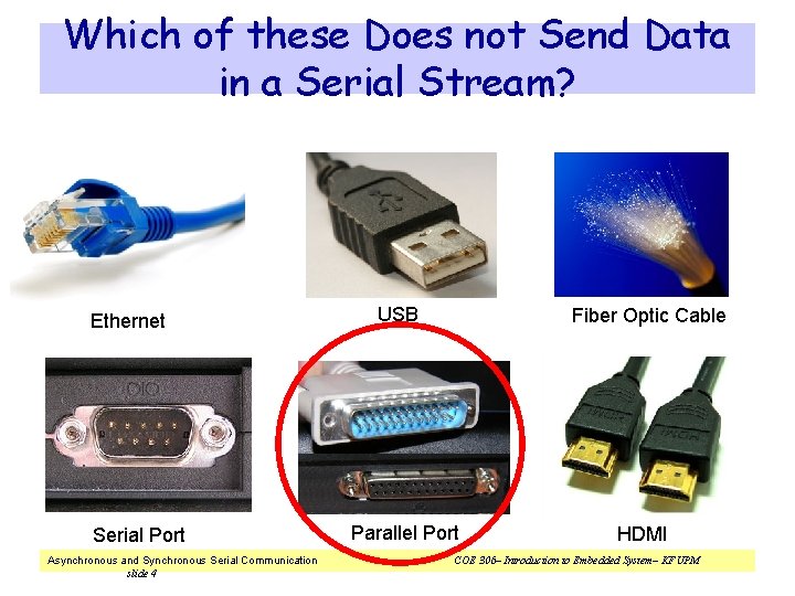
Which of these Does not Send Data in a Serial Stream? Ethernet Serial Port Asynchronous and Synchronous Serial Communication slide 4 USB Fiber Optic Cable Parallel Port HDMI COE 306– Introduction to Embedded System– KFUPM

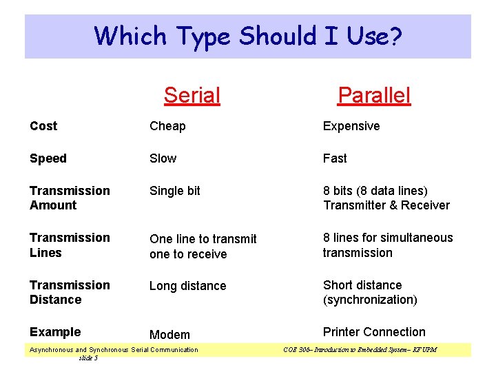
Which Type Should I Use? Serial Parallel Cost Cheap Expensive Speed Slow Fast Transmission Amount Single bit 8 bits (8 data lines) Transmitter & Receiver Transmission Lines One line to transmit one to receive 8 lines for simultaneous transmission Transmission Distance Long distance Short distance (synchronization) Example Modem Printer Connection Asynchronous and Synchronous Serial Communication slide 5 COE 306– Introduction to Embedded System– KFUPM

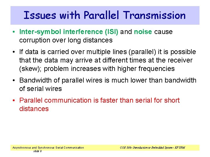
Issues with Parallel Transmission • Inter-symbol interference (ISI) and noise cause corruption over long distances • If data is carried over multiple lines (parallel) it is possible that the data may arrive at different times at the receiver (skew); problem increases with higher frequencies • Bandwidth of parallel wires is much lower than bandwidth of serial wires • Parallel communication is faster than serial for short distances Asynchronous and Synchronous Serial Communication slide 6 COE 306– Introduction to Embedded System– KFUPM

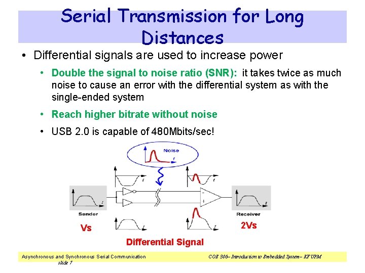
Serial Transmission for Long Distances • Differential signals are used to increase power • Double the signal to noise ratio (SNR): it takes twice as much noise to cause an error with the differential system as with the single-ended system • Reach higher bitrate without noise • USB 2. 0 is capable of 480 Mbits/sec! 2 Vs Vs Differential Signal Asynchronous and Synchronous Serial Communication slide 7 COE 306– Introduction to Embedded System– KFUPM

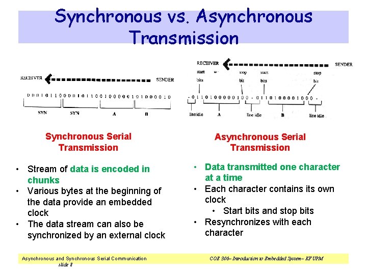
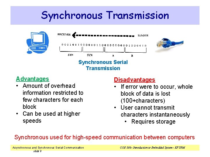
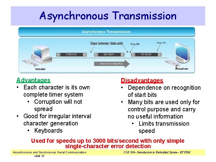
Synchronous vs. Asynchronous Transmission Synchronous Serial Transmission • Stream of data is encoded in chunks • Various bytes at the beginning of the data provide an embedded clock • The data stream can also be synchronized by an external clock Asynchronous and Synchronous Serial Communication slide 8 Asynchronous Serial Transmission • Data transmitted one character at a time • Each character contains its own clock • Start bits and stop bits • Resynchronizes with each character COE 306– Introduction to Embedded System– KFUPM

Synchronous Transmission Synchronous Serial Transmission Advantages • Amount of overhead information restricted to few characters for each block • Can be used at higher speeds Disadvantages • If error were to occur, whole block of data is lost (100+characters) • User cannot transmit characters instantaneously • Requires storage Synchronous used for high-speed communication between computers Asynchronous and Synchronous Serial Communication slide 9 COE 306– Introduction to Embedded System– KFUPM

Asynchronous Transmission Advantages • Each character is its own complete timer system • Corruption will not spread • Good for irregular interval character generation • Keyboards Disadvantages • Dependence on recognition of start bits • Many bits are used only for control purpose and carry no useful information • Limits transmission speed Used for speeds up to 3000 bits/second with only simple single-character error detection Asynchronous and Synchronous Serial Communication slide 10 COE 306– Introduction to Embedded System– KFUPM

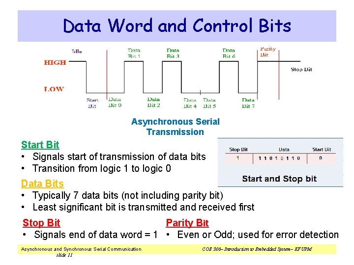
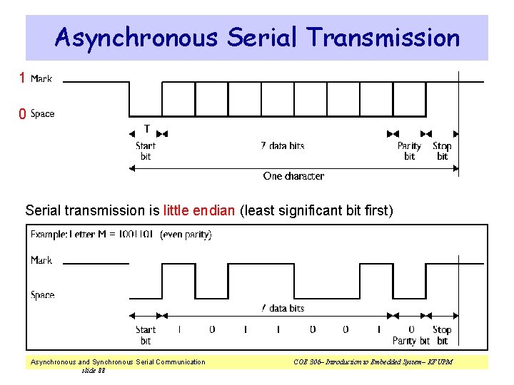
Data Word and Control Bits Asynchronous Serial Transmission Start Bit • Signals start of transmission of data bits • Transition from logic 1 to logic 0 Data Bits • Typically 7 data bits (not including parity bit) • Least significant bit is transmitted and received first Stop Bit Parity Bit • Signals end of data word = 1 • Even or Odd; used for error detection Asynchronous and Synchronous Serial Communication slide 11 COE 306– Introduction to Embedded System– KFUPM

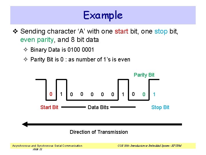
Example v Sending character ‘A’ with one start bit, one stop bit, even parity, and 8 bit data ² Binary Data is 0100 0001 ² Parity Bit is 0 : as number of 1’s is even Parity Bit 0 1 0 0 0 1 Stop Bit Data Bits Start Bit 0 Direction of Transmission Asynchronous and Synchronous Serial Communication slide 12 COE 306– Introduction to Embedded System– KFUPM

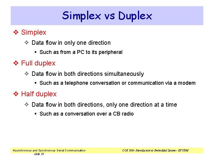
Simplex vs Duplex v Simplex ² Data flow in only one direction § Such as from a PC to its peripheral v Full duplex ² Data flow in both directions simultaneously § Such as a telephone conversation or communication via a modem v Half duplex ² Data flow in both directions, only one direction at a time § Such as a conversation over a CB radio Asynchronous and Synchronous Serial Communication slide 13 COE 306– Introduction to Embedded System– KFUPM

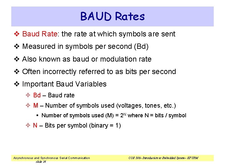
BAUD Rates v Baud Rate: the rate at which symbols are sent v Measured in symbols per second (Bd) v Also known as baud or modulation rate v Often incorrectly referred to as bits per second v Important Baud Variables ² Bd – Baud rate ² M – Number of symbols used (voltages, tones, etc. ) § Number of symbols used (M) = 2 N where N = bits / symbol ² N – Bits per symbol (binary = 1) Asynchronous and Synchronous Serial Communication slide 14 COE 306– Introduction to Embedded System– KFUPM

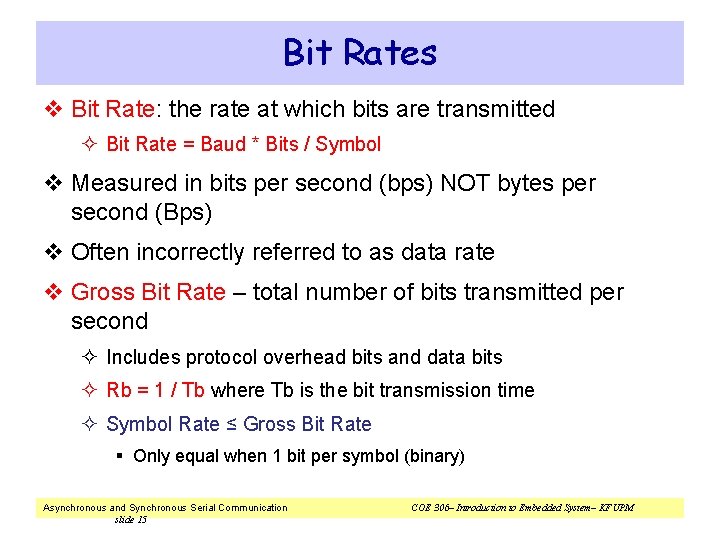
Bit Rates v Bit Rate: the rate at which bits are transmitted ² Bit Rate = Baud * Bits / Symbol v Measured in bits per second (bps) NOT bytes per second (Bps) v Often incorrectly referred to as data rate v Gross Bit Rate – total number of bits transmitted per second ² Includes protocol overhead bits and data bits ² Rb = 1 / Tb where Tb is the bit transmission time ² Symbol Rate ≤ Gross Bit Rate § Only equal when 1 bit per symbol (binary) Asynchronous and Synchronous Serial Communication slide 15 COE 306– Introduction to Embedded System– KFUPM

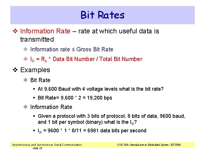
Bit Rates v Information Rate – rate at which useful data is transmitted ² Information rate ≤ Gross Bit Rate ² IR = Rb * Data Bit Number / Total Bit Number v Examples ² Bit Rate § At 9, 600 Baud with 4 voltage levels what is the bit rate? § Bit Rate= 9, 600 * 2 = 19, 200 bps ² Information Rate § Given a protocol with 3 bits of protocol, 8 bits of data, 9600 baud, and 1 bit per symbol (binary) what is the IR? § IR = 9600 * 1 * 8/11 = 6981 data bits per second Asynchronous and Synchronous Serial Communication slide 16 COE 306– Introduction to Embedded System– KFUPM

Serial Transmission Interfaces v Synchronous ² Serial Peripheral Interface (SPI) ² Inter-Integrated Circuit (I²C) v Asynchronous ² Universal Asynchronous Receiver Transmitter (UART) Asynchronous and Synchronous Serial Communication slide 17 COE 306– Introduction to Embedded System– KFUPM

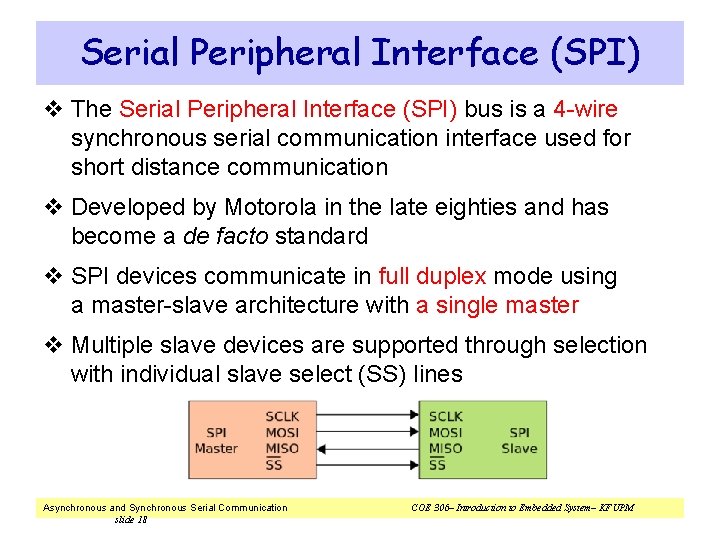
Serial Peripheral Interface (SPI) v The Serial Peripheral Interface (SPI) bus is a 4 -wire synchronous serial communication interface used for short distance communication v Developed by Motorola in the late eighties and has become a de facto standard v SPI devices communicate in full duplex mode using a master-slave architecture with a single master v Multiple slave devices are supported through selection with individual slave select (SS) lines Asynchronous and Synchronous Serial Communication slide 18 COE 306– Introduction to Embedded System– KFUPM

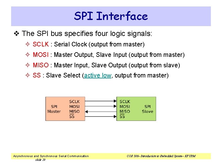
SPI Interface v The SPI bus specifies four logic signals: ² SCLK : Serial Clock (output from master) ² MOSI : Master Output, Slave Input (output from master) ² MISO : Master Input, Slave Output (output from slave) ² SS : Slave Select (active low, output from master) Asynchronous and Synchronous Serial Communication slide 19 COE 306– Introduction to Embedded System– KFUPM

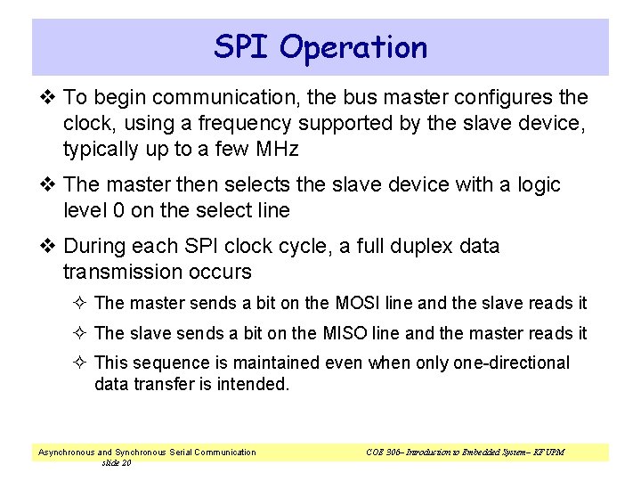
SPI Operation v To begin communication, the bus master configures the clock, using a frequency supported by the slave device, typically up to a few MHz v The master then selects the slave device with a logic level 0 on the select line v During each SPI clock cycle, a full duplex data transmission occurs ² The master sends a bit on the MOSI line and the slave reads it ² The slave sends a bit on the MISO line and the master reads it ² This sequence is maintained even when only one-directional data transfer is intended. Asynchronous and Synchronous Serial Communication slide 20 COE 306– Introduction to Embedded System– KFUPM

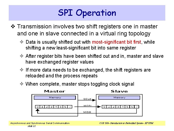
SPI Operation v Transmission involves two shift registers one in master and one in slave connected in a virtual ring topology ² Data is usually shifted out with most-significant bit first, while shifting a new least-significant bit into same register ² After register bits have been shifted out and in, master and slave have exchanged register values ² If more data needs to be exchanged, the shift registers are reloaded and the process repeats ² When complete, master stops toggling clock signal Asynchronous and Synchronous Serial Communication slide 21 COE 306– Introduction to Embedded System– KFUPM

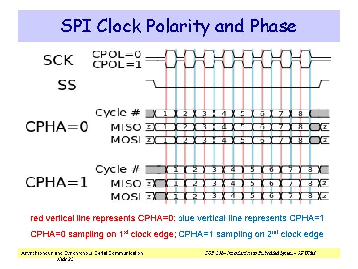
SPI Clock Polarity and Phase v In addition to setting clock frequency, master must also configure clock polarity (CPOL) and phase (CPHA) ² At CPOL=0 the base value of the clock is zero, i. e. the idle state is 0 and active state is 1 § For CPHA=0, data are captured on the clock's rising edge (low→high transition) and data is output on a falling edge (high→low clock transition) § For CPHA=1, data are captured on the clock's falling edge and data is output on a rising edge ² At CPOL=1 the base value of the clock is one (inversion of CPOL=0), i. e. the idle state is 1 and active state is 0 § For CPHA=0, data are captured on clock's falling edge and data is output on a rising edge § For CPHA=1, data are captured on clock's rising edge and data is output on a falling edge Asynchronous and Synchronous Serial Communication slide 22 COE 306– Introduction to Embedded System– KFUPM

SPI Clock Polarity and Phase red vertical line represents CPHA=0; blue vertical line represents CPHA=1 CPHA=0 sampling on 1 st clock edge; CPHA=1 sampling on 2 nd clock edge Asynchronous and Synchronous Serial Communication slide 23 COE 306– Introduction to Embedded System– KFUPM

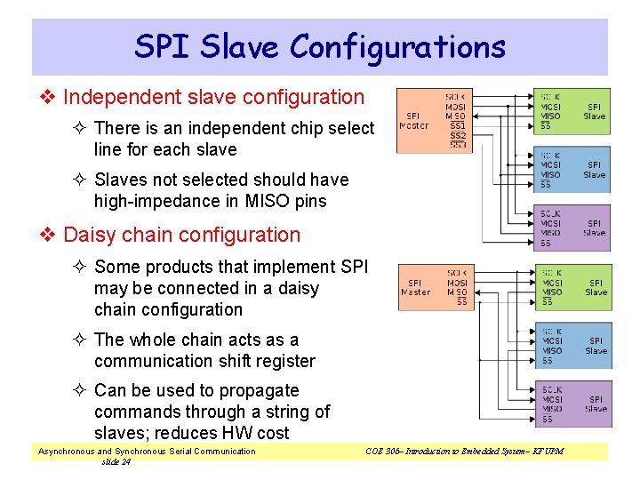
SPI Slave Configurations v Independent slave configuration ² There is an independent chip select line for each slave ² Slaves not selected should have high-impedance in MISO pins v Daisy chain configuration ² Some products that implement SPI may be connected in a daisy chain configuration ² The whole chain acts as a communication shift register ² Can be used to propagate commands through a string of slaves; reduces HW cost Asynchronous and Synchronous Serial Communication slide 24 COE 306– Introduction to Embedded System– KFUPM

SPI Applications v SPI is used to talk to a variety of peripherals, such as ² Sensors: temperature, pressure, touchscreens ² Control devices: audio codecs, digital potentiometers, DAC ² Camera lenses: Canon EF lens mount ² Memory: flash and EEPROM ² Real-time clocks ² LCD, sometimes even for managing image data ² Any MMC or SD card Asynchronous and Synchronous Serial Communication slide 25 COE 306– Introduction to Embedded System– KFUPM

SPI Advantages v Full duplex communication v Higher throughput than I²C or SMBus v Complete protocol flexibility for the bits transferred v Extremely simple hardware interfacing v Uses only four pins on IC packages v At most one unique bus signal per device (chip select) v Not limited to any maximum clock speed, enabling potentially high speed v Simple software implementation Asynchronous and Synchronous Serial Communication slide 26 COE 306– Introduction to Embedded System– KFUPM

SPI Disadvantages v Requires more pins on IC packages than I²C v No hardware flow control by the slave (but the master can delay the next clock edge to slow the transfer rate) v No hardware slave acknowledgment (the master could be transmitting to nowhere and not know it) v Typically supports only one master device (depends on device's hardware implementation) v No error-checking protocol is defined v Only handles short distances compared to RS-232, RS 485, or CAN-bus Asynchronous and Synchronous Serial Communication slide 27 COE 306– Introduction to Embedded System– KFUPM

LPC 176 x/5 x SPI Interface (SSP 0/1) v The SSP is a Synchronous Serial Port (SSP) controller capable of operation on a SPI, 4 -wire SSI, or Microwire bus. v It can interact with multiple masters and slaves on bus. v Only a single master and a single slave can communicate on the bus during a given data transfer. v Data transfers are in principle full duplex, with frames of 4 to 16 bits of data flowing from the master to the slave and from the slave to the master. v Maximum data bit rate of one eighth of the peripheral clock rate. v 8 frame FIFOs for both transmit and receive. Asynchronous and Synchronous Serial Communication slide 28 COE 306– Introduction to Embedded System– KFUPM

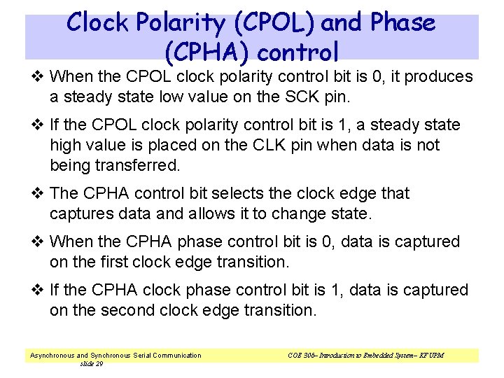
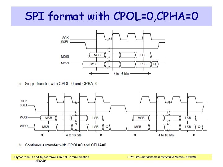
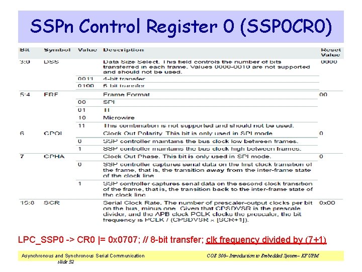
Clock Polarity (CPOL) and Phase (CPHA) control v When the CPOL clock polarity control bit is 0, it produces a steady state low value on the SCK pin. v If the CPOL clock polarity control bit is 1, a steady state high value is placed on the CLK pin when data is not being transferred. v The CPHA control bit selects the clock edge that captures data and allows it to change state. v When the CPHA phase control bit is 0, data is captured on the first clock edge transition. v If the CPHA clock phase control bit is 1, data is captured on the second clock edge transition. Asynchronous and Synchronous Serial Communication slide 29 COE 306– Introduction to Embedded System– KFUPM

SPI format with CPOL=0, CPHA=0 Asynchronous and Synchronous Serial Communication slide 30 COE 306– Introduction to Embedded System– KFUPM

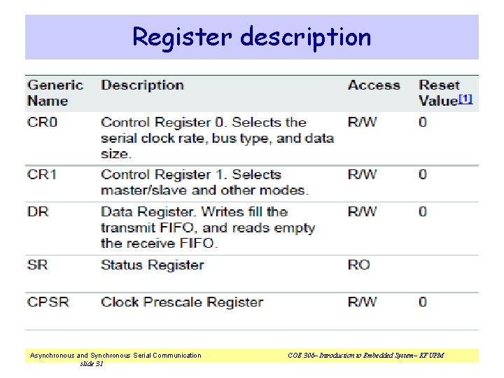
Register description Asynchronous and Synchronous Serial Communication slide 31 COE 306– Introduction to Embedded System– KFUPM

SSPn Control Register 0 (SSP 0 CR 0) LPC_SSP 0 -> CR 0 |= 0 x 0707; // 8 -bit transfer; clk frequency divided by (7+1) Asynchronous and Synchronous Serial Communication slide 32 COE 306– Introduction to Embedded System– KFUPM

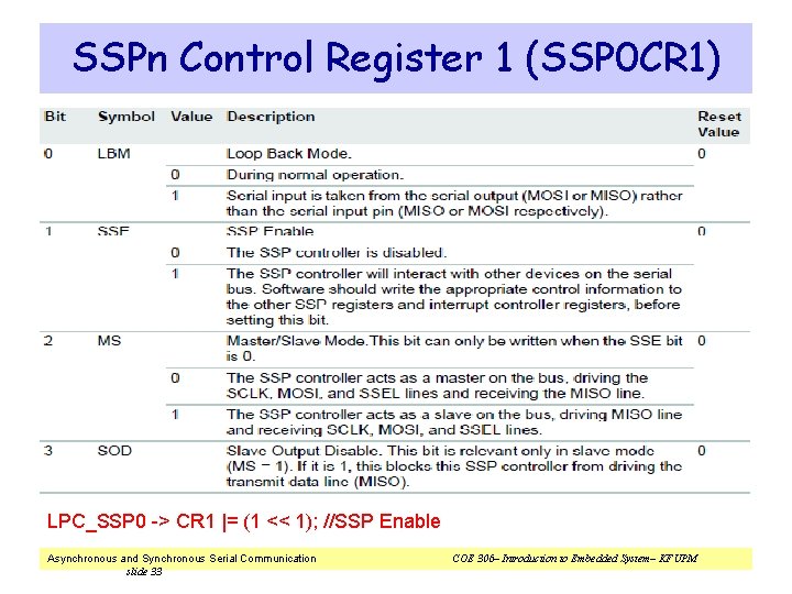
SSPn Control Register 1 (SSP 0 CR 1) LPC_SSP 0 -> CR 1 |= (1 << 1); //SSP Enable Asynchronous and Synchronous Serial Communication slide 33 COE 306– Introduction to Embedded System– KFUPM

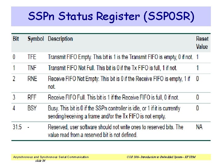
SSPn Status Register (SSP 0 SR) Asynchronous and Synchronous Serial Communication slide 34 COE 306– Introduction to Embedded System– KFUPM

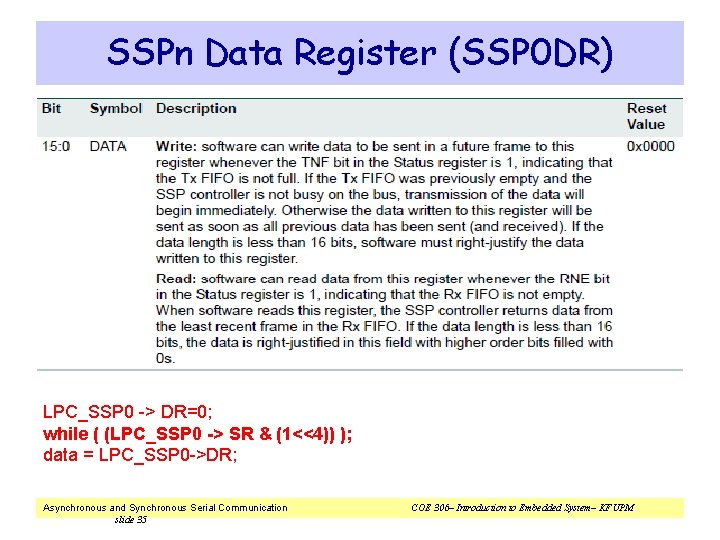
SSPn Data Register (SSP 0 DR) LPC_SSP 0 -> DR=0; while ( (LPC_SSP 0 -> SR & (1<<4)) ); data = LPC_SSP 0 ->DR; Asynchronous and Synchronous Serial Communication slide 35 COE 306– Introduction to Embedded System– KFUPM

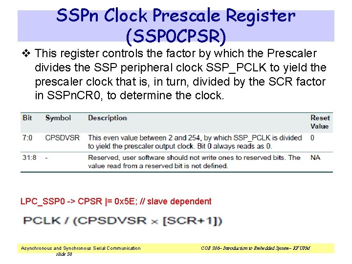
SSPn Clock Prescale Register (SSP 0 CPSR) v This register controls the factor by which the Prescaler divides the SSP peripheral clock SSP_PCLK to yield the prescaler clock that is, in turn, divided by the SCR factor in SSPn. CR 0, to determine the clock. LPC_SSP 0 -> CPSR |= 0 x 5 E; // slave dependent Asynchronous and Synchronous Serial Communication slide 36 COE 306– Introduction to Embedded System– KFUPM

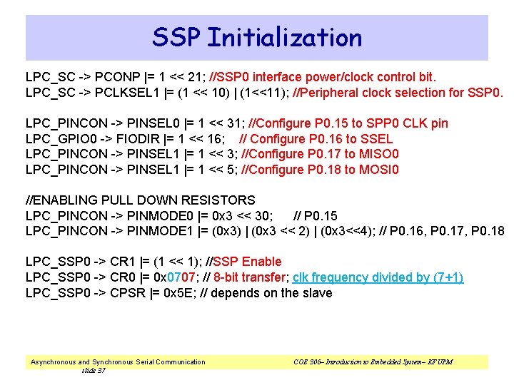
SSP Initialization LPC_SC -> PCONP |= 1 << 21; //SSP 0 interface power/clock control bit. LPC_SC -> PCLKSEL 1 |= (1 << 10) | (1<<11); //Peripheral clock selection for SSP 0. LPC_PINCON -> PINSEL 0 |= 1 << 31; //Configure P 0. 15 to SPP 0 CLK pin LPC_GPIO 0 -> FIODIR |= 1 << 16; // Configure P 0. 16 to SSEL LPC_PINCON -> PINSEL 1 |= 1 << 3; //Configure P 0. 17 to MISO 0 LPC_PINCON -> PINSEL 1 |= 1 << 5; //Configure P 0. 18 to MOSI 0 //ENABLING PULL DOWN RESISTORS LPC_PINCON -> PINMODE 0 |= 0 x 3 << 30; // P 0. 15 LPC_PINCON -> PINMODE 1 |= (0 x 3) | (0 x 3 << 2) | (0 x 3<<4); // P 0. 16, P 0. 17, P 0. 18 LPC_SSP 0 -> CR 1 |= (1 << 1); //SSP Enable LPC_SSP 0 -> CR 0 |= 0 x 0707; // 8 -bit transfer; clk frequency divided by (7+1) LPC_SSP 0 -> CPSR |= 0 x 5 E; // depends on the slave Asynchronous and Synchronous Serial Communication slide 37 COE 306– Introduction to Embedded System– KFUPM

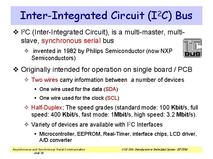
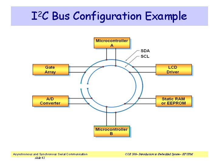
Inter-Integrated Circuit (I 2 C) Bus v I²C (Inter-Integrated Circuit), is a multi-master, multislave, synchronous serial bus ² invented in 1982 by Philips Semiconductor (now NXP Semiconductors) v Originally intended for operation on single board / PCB ² Two wires carry information between a number of devices § One wire used for the data (SDA) § One wire used for the clock (SCL) ² Half-Duplex; The speed grades (standard mode: 100 Kbit/s, full speed: 400 Kbit/s, fast mode: 1 Mbit/s, high speed: 3. 2 Mbit/s). ² Variety of devices are available with I 2 C Interfaces § Microcontroller, EEPROM, Real-Timer, interface chips, LCD driver, A/D converter Asynchronous and Synchronous Serial Communication slide 38 COE 306– Introduction to Embedded System– KFUPM

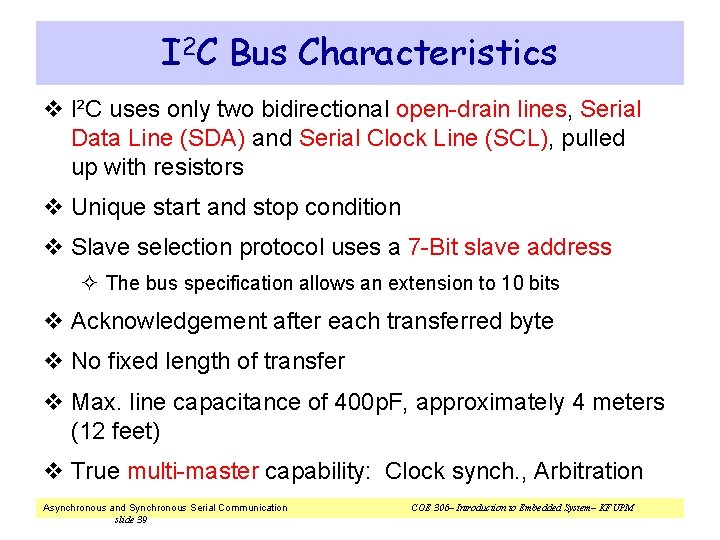
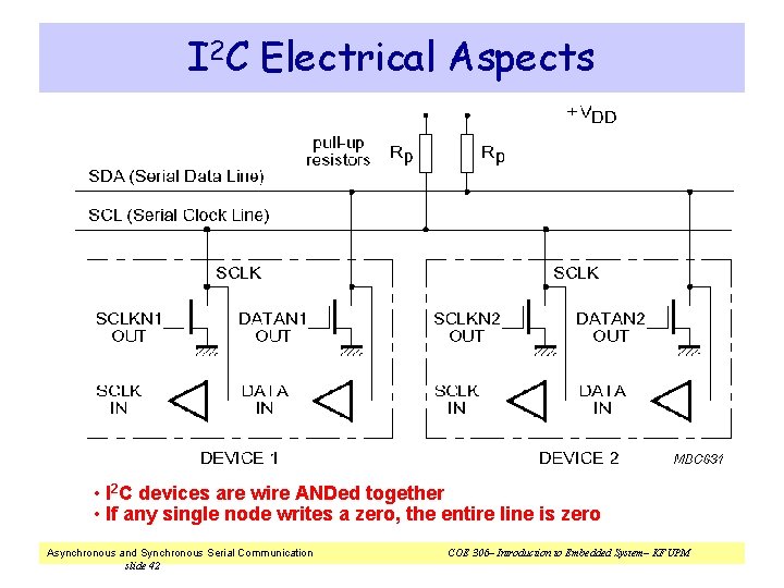
I 2 C Bus Characteristics v I²C uses only two bidirectional open-drain lines, Serial Data Line (SDA) and Serial Clock Line (SCL), pulled up with resistors v Unique start and stop condition v Slave selection protocol uses a 7 -Bit slave address ² The bus specification allows an extension to 10 bits v Acknowledgement after each transferred byte v No fixed length of transfer v Max. line capacitance of 400 p. F, approximately 4 meters (12 feet) v True multi-master capability: Clock synch. , Arbitration Asynchronous and Synchronous Serial Communication slide 39 COE 306– Introduction to Embedded System– KFUPM

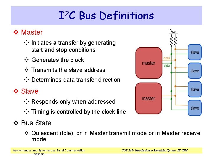
I 2 C Bus Definitions v Master ² Initiates a transfer by generating start and stop conditions ² Generates the clock ² Transmits the slave address ² Determines data transfer direction v Slave ² Responds only when addressed ² Timing is controlled by the clock line v Bus State ² Quiescent (Idle), or in Master transmit mode or in Master receive mode Asynchronous and Synchronous Serial Communication slide 40 COE 306– Introduction to Embedded System– KFUPM

I 2 C Bus Configuration Example Asynchronous and Synchronous Serial Communication slide 41 COE 306– Introduction to Embedded System– KFUPM

I 2 C Electrical Aspects • I 2 C devices are wire ANDed together • If any single node writes a zero, the entire line is zero Asynchronous and Synchronous Serial Communication slide 42 COE 306– Introduction to Embedded System– KFUPM

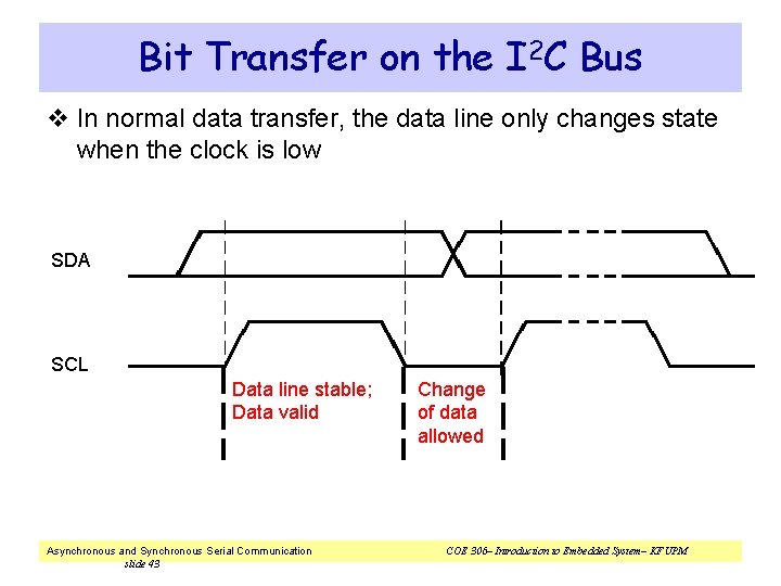
Bit Transfer on the I 2 C Bus v In normal data transfer, the data line only changes state when the clock is low SDA SCL Data line stable; Data valid Asynchronous and Synchronous Serial Communication slide 43 Change of data allowed COE 306– Introduction to Embedded System– KFUPM

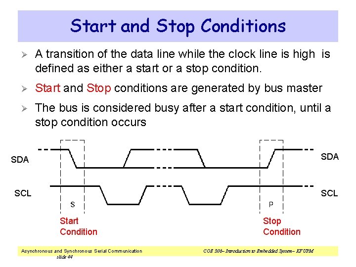
Start and Stop Conditions Ø A transition of the data line while the clock line is high is defined as either a start or a stop condition. Ø Start and Stop conditions are generated by bus master Ø The bus is considered busy after a start condition, until a stop condition occurs SDA SCL Start Condition Asynchronous and Synchronous Serial Communication slide 44 Stop Condition COE 306– Introduction to Embedded System– KFUPM

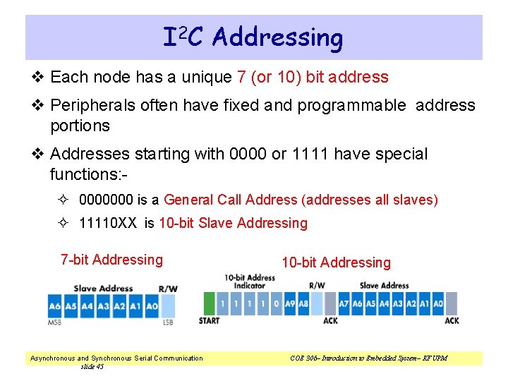
I 2 C Addressing v Each node has a unique 7 (or 10) bit address v Peripherals often have fixed and programmable address portions v Addresses starting with 0000 or 1111 have special functions: - ² 0000000 is a General Call Address (addresses all slaves) ² 11110 XX is 10 -bit Slave Addressing 7 -bit Addressing Asynchronous and Synchronous Serial Communication slide 45 10 -bit Addressing COE 306– Introduction to Embedded System– KFUPM

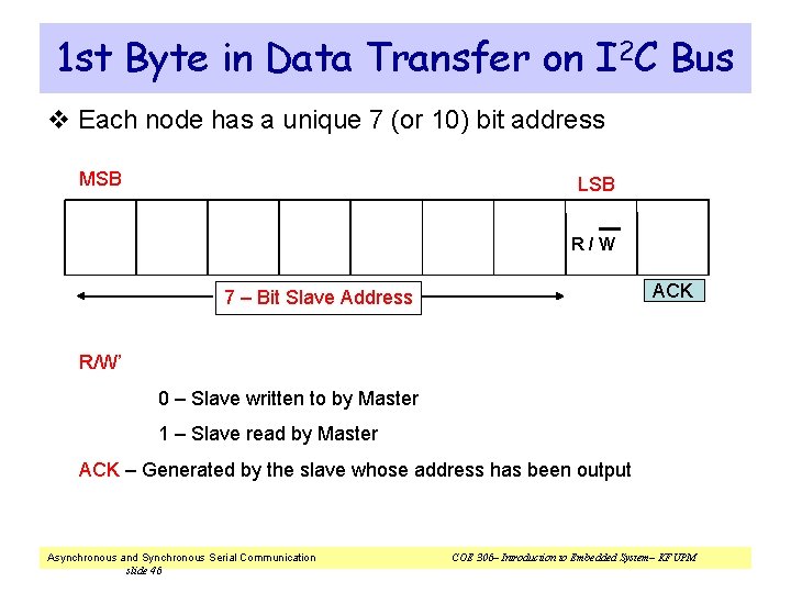
1 st Byte in Data Transfer on I 2 C Bus v Each node has a unique 7 (or 10) bit address MSB LSB R/W ACK 7 – Bit Slave Address R/W’ 0 – Slave written to by Master 1 – Slave read by Master ACK – Generated by the slave whose address has been output Asynchronous and Synchronous Serial Communication slide 46 COE 306– Introduction to Embedded System– KFUPM

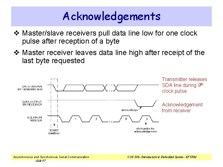
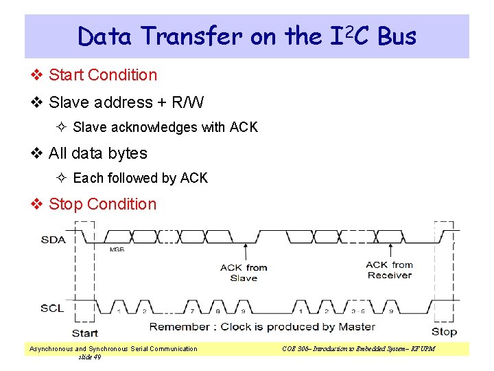
Acknowledgements v Master/slave receivers pull data line low for one clock pulse after reception of a byte v Master receiver leaves data line high after receipt of the last byte requested Transmitter releases SDA line during 9 th clock pulse. Acknowledgement from receiver Asynchronous and Synchronous Serial Communication slide 47 COE 306– Introduction to Embedded System– KFUPM

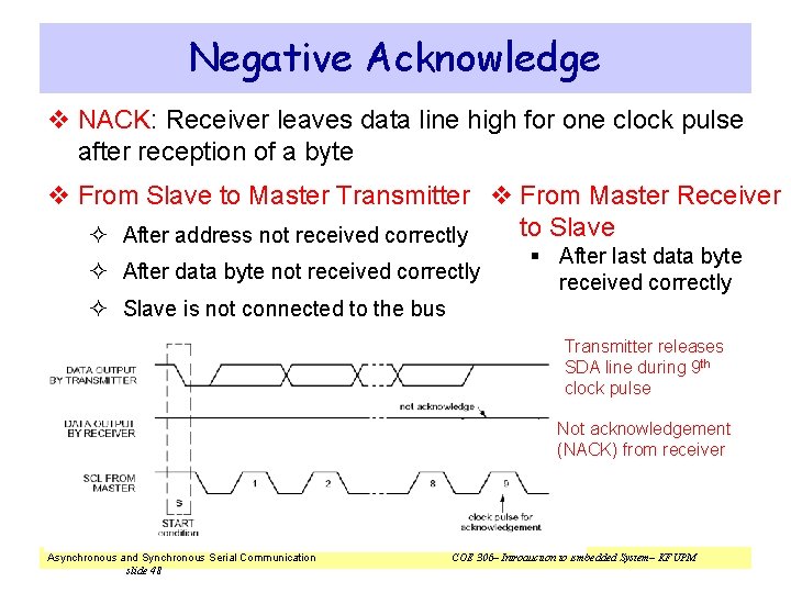
Negative Acknowledge v NACK: Receiver leaves data line high for one clock pulse after reception of a byte v From Slave to Master Transmitter v From Master Receiver to Slave ² After address not received correctly ² After data byte not received correctly § After last data byte received correctly ² Slave is not connected to the bus Transmitter releases SDA line during 9 th clock pulse Not acknowledgement (NACK) from receiver Asynchronous and Synchronous Serial Communication slide 48 COE 306– Introduction to Embedded System– KFUPM

Data Transfer on the I 2 C Bus v Start Condition v Slave address + R/W ² Slave acknowledges with ACK v All data bytes ² Each followed by ACK v Stop Condition Asynchronous and Synchronous Serial Communication slide 49 COE 306– Introduction to Embedded System– KFUPM

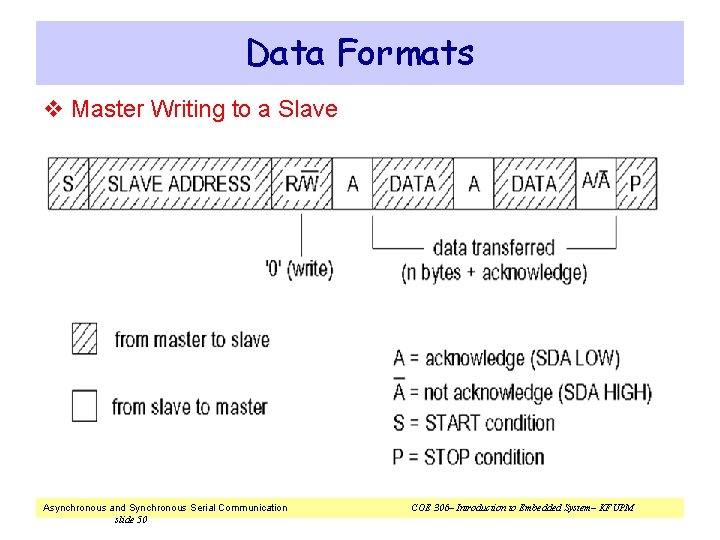
Data Formats v Master Writing to a Slave Asynchronous and Synchronous Serial Communication slide 50 COE 306– Introduction to Embedded System– KFUPM

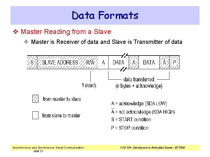
Data Formats v Master Reading from a Slave ² Master is Receiver of data and Slave is Transmitter of data 1 Asynchronous and Synchronous Serial Communication slide 51 COE 306– Introduction to Embedded System– KFUPM

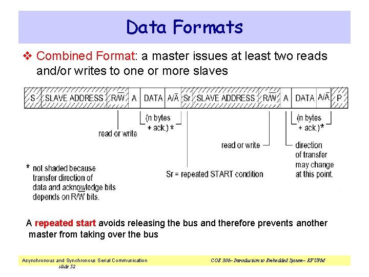
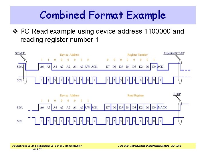
Data Formats v Combined Format: a master issues at least two reads and/or writes to one or more slaves A repeated start avoids releasing the bus and therefore prevents another master from taking over the bus Asynchronous and Synchronous Serial Communication slide 52 COE 306– Introduction to Embedded System– KFUPM

Combined Format Example v I 2 C Read example using device address 1100000 and reading register number 1 Asynchronous and Synchronous Serial Communication slide 53 COE 306– Introduction to Embedded System– KFUPM

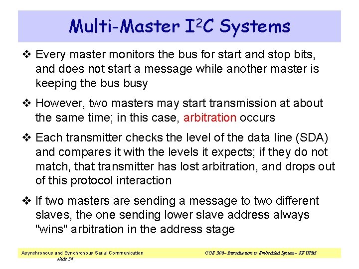
Multi-Master I 2 C Systems v Every master monitors the bus for start and stop bits, and does not start a message while another master is keeping the busy v However, two masters may start transmission at about the same time; in this case, arbitration occurs v Each transmitter checks the level of the data line (SDA) and compares it with the levels it expects; if they do not match, that transmitter has lost arbitration, and drops out of this protocol interaction v If two masters are sending a message to two different slaves, the one sending lower slave address always "wins" arbitration in the address stage Asynchronous and Synchronous Serial Communication slide 54 COE 306– Introduction to Embedded System– KFUPM

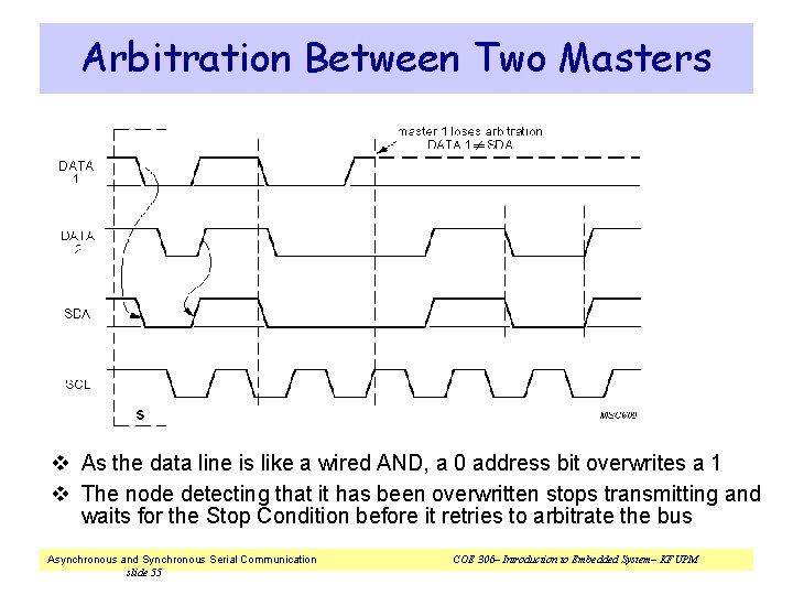
Arbitration Between Two Masters v As the data line is like a wired AND, a 0 address bit overwrites a 1 v The node detecting that it has been overwritten stops transmitting and waits for the Stop Condition before it retries to arbitrate the bus Asynchronous and Synchronous Serial Communication slide 55 COE 306– Introduction to Embedded System– KFUPM

I 2 C Bus Advantages v Simple 2 -wire serial I 2 C-bus minimizes interconnections v ICs can be added to or removed from a system without affecting any other circuits on the bus v The multi-master capability of the I 2 C-bus allows rapid testing/alignment of end-user equipment via external connections to an assembly-line v Incorporates ACK/NACK functionality for improved error handling v The I 2 C-bus is a de facto world standard that is implemented in over 1000 different ICs (Philips has > 400) and licensed to more than 70 companies Asynchronous and Synchronous Serial Communication slide 56 COE 306– Introduction to Embedded System– KFUPM

I 2 C Bus Disadvantages v The assignment of slave addresses is one weakness of I²C v Imposes protocol overhead that reduces throughput v Because I²C is a shared bus, there is the potential for any device to have a fault and hang the entire bus v I²C supports a limited range of speeds v Requires pull-up resistors, which ² limit clock speed ² consume valuable PCB real estate in extremely spaceconstrained systems ² increase power dissipation Asynchronous and Synchronous Serial Communication slide 57 COE 306– Introduction to Embedded System– KFUPM

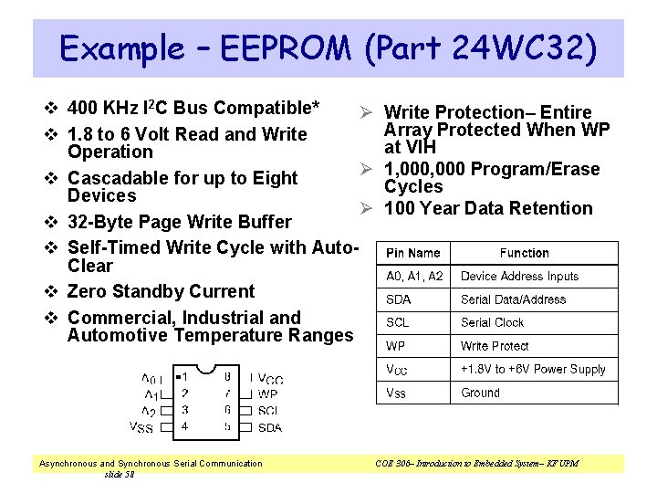
Example – EEPROM (Part 24 WC 32) v 400 KHz I 2 C Bus Compatible* Ø v 1. 8 to 6 Volt Read and Write Operation Ø v Cascadable for up to Eight Devices Ø v 32 -Byte Page Write Buffer v Self-Timed Write Cycle with Auto. Clear v Zero Standby Current v Commercial, Industrial and Automotive Temperature Ranges Asynchronous and Synchronous Serial Communication slide 58 Write Protection– Entire Array Protected When WP at VIH 1, 000 Program/Erase Cycles 100 Year Data Retention COE 306– Introduction to Embedded System– KFUPM

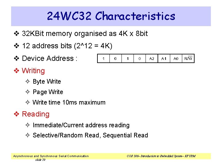
24 WC 32 Characteristics v 32 KBit memory organised as 4 K x 8 bit v 12 address bits (2^12 = 4 K) v Device Address : v Writing ² Byte Write ² Page Write ² Write time 10 ms maximum v Reading ² Immediate/Current address reading ² Selective/Random Read, Sequential Read Asynchronous and Synchronous Serial Communication slide 59 COE 306– Introduction to Embedded System– KFUPM

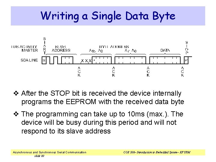
Writing a Single Data Byte v After the STOP bit is received the device internally programs the EEPROM with the received data byte v The programming can take up to 10 ms (max. ). The device will be busy during this period and will not respond to its slave address Asynchronous and Synchronous Serial Communication slide 60 COE 306– Introduction to Embedded System– KFUPM

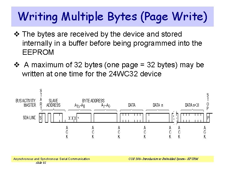
Writing Multiple Bytes (Page Write) v The bytes are received by the device and stored internally in a buffer before being programmed into the EEPROM v A maximum of 32 bytes (one page = 32 bytes) may be written at one time for the 24 WC 32 device Asynchronous and Synchronous Serial Communication slide 61 COE 306– Introduction to Embedded System– KFUPM

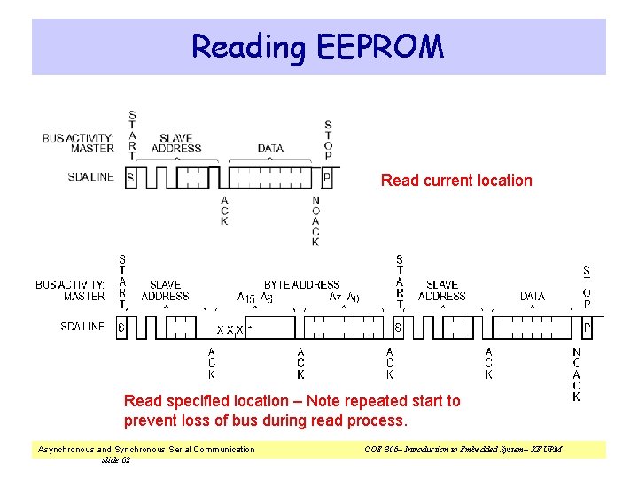
Reading EEPROM Read current location Read specified location – Note repeated start to prevent loss of bus during read process. Asynchronous and Synchronous Serial Communication slide 62 COE 306– Introduction to Embedded System– KFUPM

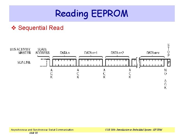
Reading EEPROM v Sequential Read Asynchronous and Synchronous Serial Communication slide 63 COE 306– Introduction to Embedded System– KFUPM

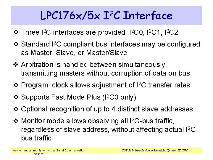
LPC 176 x/5 x I 2 C Interface v Three I 2 C interfaces are provided: I 2 C 0, I 2 C 1, I 2 C 2 v Standard I 2 C compliant bus interfaces may be configured as Master, Slave, or Master/Slave v Arbitration is handled between simultaneously transmitting masters without corruption of data on bus v Program. clock allows adjustment of I 2 C transfer rates v Supports Fast Mode Plus (I 2 C 0 only) v Optional recognition of up to 4 distinct slave addresses v Monitor mode allows observing all I 2 C-bus traffic, regardless of slave address, without affecting actual I 2 Cbus traffic Asynchronous and Synchronous Serial Communication slide 64 COE 306– Introduction to Embedded System– KFUPM

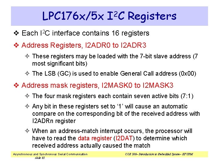
LPC 176 x/5 x I 2 C Registers v Each I 2 C interface contains 16 registers v Address Registers, I 2 ADR 0 to I 2 ADR 3 ² These registers may be loaded with the 7 -bit slave address (7 most significant bits) ² The LSB (GC) is used to enable General Call address (0 x 00) v Address mask registers, I 2 MASK 0 to I 2 MASK 3 ² The four mask registers each contain seven active bits (7: 1) ² Any bit in these registers set to ‘ 1’ will cause an automatic compare on the corresponding bit of the received address with I 2 ADRn register ² When an address-match interrupt occurs, the processor will have to read the data register (I 2 DAT) to determine which received address actually caused the match Asynchronous and Synchronous Serial Communication slide 65 COE 306– Introduction to Embedded System– KFUPM

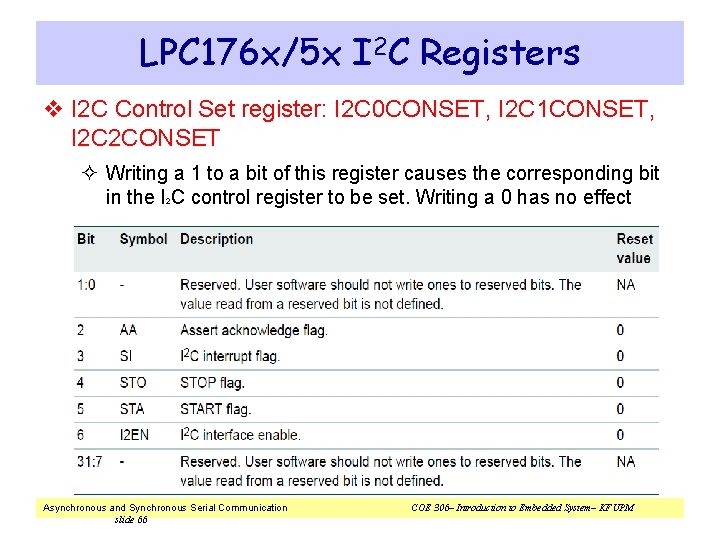
LPC 176 x/5 x I 2 C Registers v I 2 C Control Set register: I 2 C 0 CONSET, I 2 C 1 CONSET, I 2 C 2 CONSET ² Writing a 1 to a bit of this register causes the corresponding bit in the I C control register to be set. Writing a 0 has no effect 2 Asynchronous and Synchronous Serial Communication slide 66 COE 306– Introduction to Embedded System– KFUPM

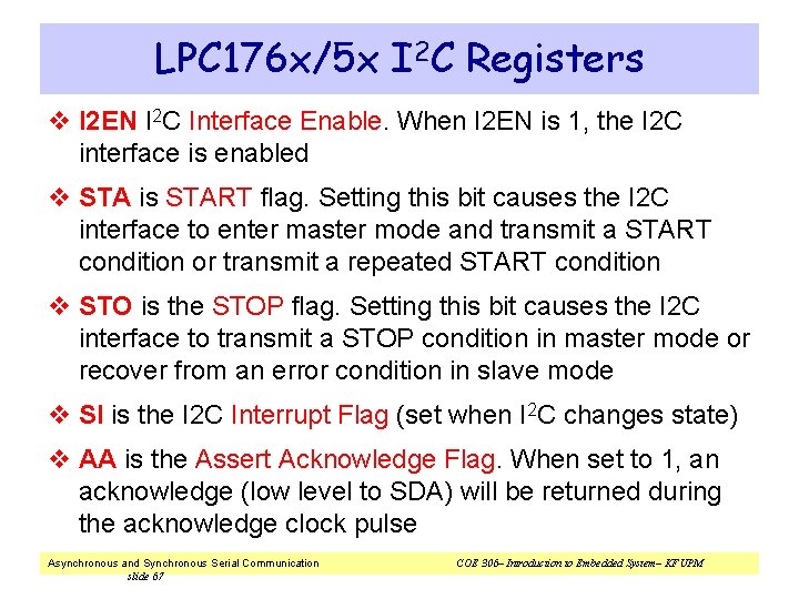
LPC 176 x/5 x I 2 C Registers v I 2 EN I 2 C Interface Enable. When I 2 EN is 1, the I 2 C interface is enabled v STA is START flag. Setting this bit causes the I 2 C interface to enter master mode and transmit a START condition or transmit a repeated START condition v STO is the STOP flag. Setting this bit causes the I 2 C interface to transmit a STOP condition in master mode or recover from an error condition in slave mode v SI is the I 2 C Interrupt Flag (set when I 2 C changes state) v AA is the Assert Acknowledge Flag. When set to 1, an acknowledge (low level to SDA) will be returned during the acknowledge clock pulse Asynchronous and Synchronous Serial Communication slide 67 COE 306– Introduction to Embedded System– KFUPM

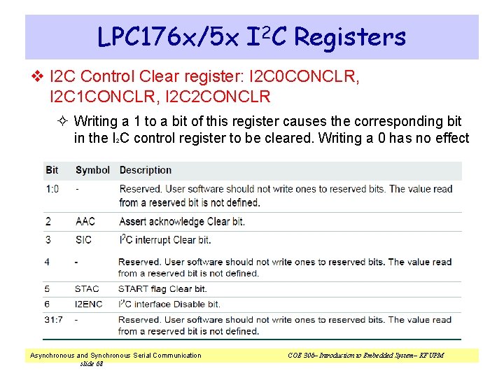
LPC 176 x/5 x I 2 C Registers v I 2 C Control Clear register: I 2 C 0 CONCLR, I 2 C 1 CONCLR, I 2 C 2 CONCLR ² Writing a 1 to a bit of this register causes the corresponding bit in the I C control register to be cleared. Writing a 0 has no effect 2 Asynchronous and Synchronous Serial Communication slide 68 COE 306– Introduction to Embedded System– KFUPM

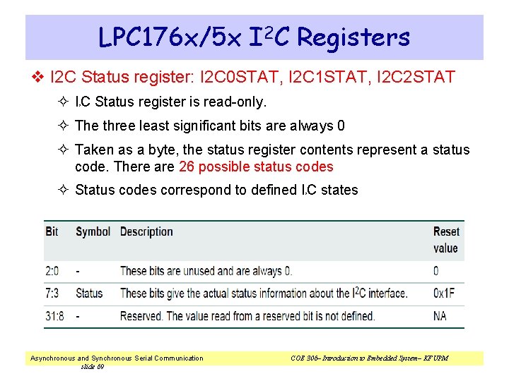
LPC 176 x/5 x I 2 C Registers v I 2 C Status register: I 2 C 0 STAT, I 2 C 1 STAT, I 2 C 2 STAT ² I C Status register is read-only. 2 ² The three least significant bits are always 0 ² Taken as a byte, the status register contents represent a status code. There are 26 possible status codes ² Status codes correspond to defined I C states 2 Asynchronous and Synchronous Serial Communication slide 69 COE 306– Introduction to Embedded System– KFUPM

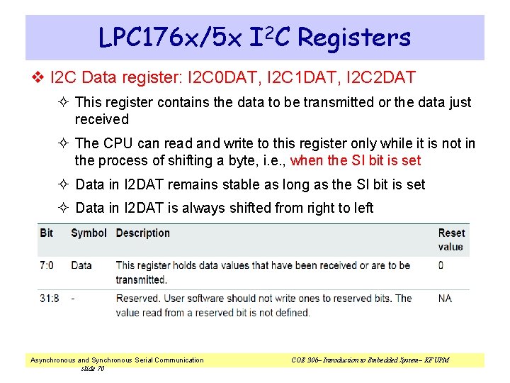
LPC 176 x/5 x I 2 C Registers v I 2 C Data register: I 2 C 0 DAT, I 2 C 1 DAT, I 2 C 2 DAT ² This register contains the data to be transmitted or the data just received ² The CPU can read and write to this register only while it is not in the process of shifting a byte, i. e. , when the SI bit is set ² Data in I 2 DAT remains stable as long as the SI bit is set ² Data in I 2 DAT is always shifted from right to left Asynchronous and Synchronous Serial Communication slide 70 COE 306– Introduction to Embedded System– KFUPM

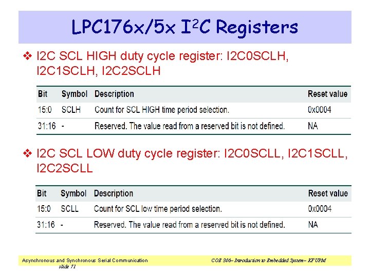
LPC 176 x/5 x I 2 C Registers v I 2 C SCL HIGH duty cycle register: I 2 C 0 SCLH, I 2 C 1 SCLH, I 2 C 2 SCLH v I 2 C SCL LOW duty cycle register: I 2 C 0 SCLL, I 2 C 1 SCLL, I 2 C 2 SCLL Asynchronous and Synchronous Serial Communication slide 71 COE 306– Introduction to Embedded System– KFUPM

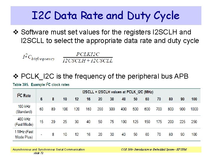
I 2 C Data Rate and Duty Cycle v Software must set values for the registers I 2 SCLH and I 2 SCLL to select the appropriate data rate and duty cycle v PCLK_I 2 C is the frequency of the peripheral bus APB Asynchronous and Synchronous Serial Communication slide 72 COE 306– Introduction to Embedded System– KFUPM

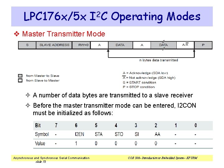
LPC 176 x/5 x I 2 C Operating Modes v Master Transmitter Mode ² A number of data bytes are transmitted to a slave receiver ² Before the master transmitter mode can be entered, I 2 CON must be initialized as follows: Asynchronous and Synchronous Serial Communication slide 73 COE 306– Introduction to Embedded System– KFUPM

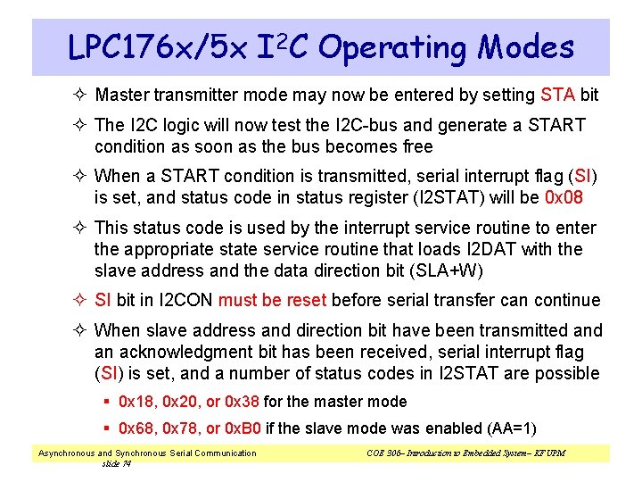
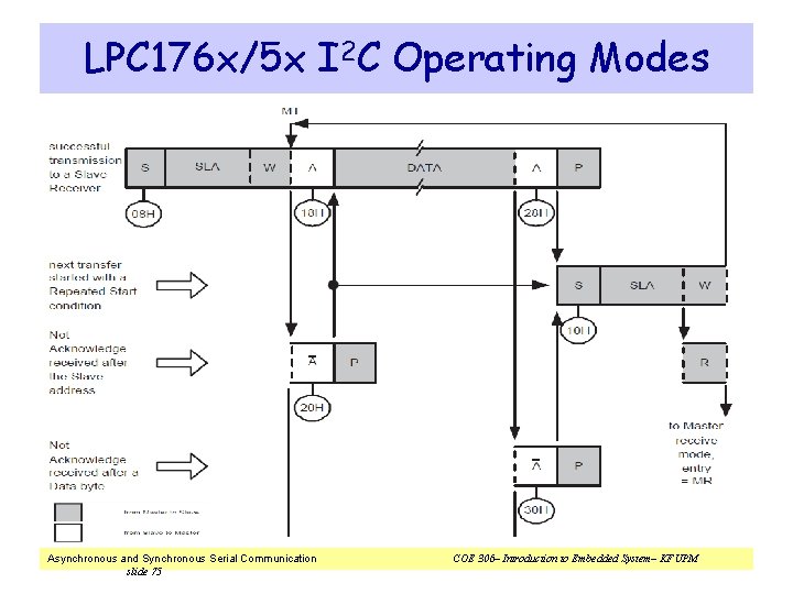
LPC 176 x/5 x I 2 C Operating Modes ² Master transmitter mode may now be entered by setting STA bit ² The I 2 C logic will now test the I 2 C-bus and generate a START condition as soon as the bus becomes free ² When a START condition is transmitted, serial interrupt flag (SI) is set, and status code in status register (I 2 STAT) will be 0 x 08 ² This status code is used by the interrupt service routine to enter the appropriate state service routine that loads I 2 DAT with the slave address and the data direction bit (SLA+W) ² SI bit in I 2 CON must be reset before serial transfer can continue ² When slave address and direction bit have been transmitted an acknowledgment bit has been received, serial interrupt flag (SI) is set, and a number of status codes in I 2 STAT are possible § 0 x 18, 0 x 20, or 0 x 38 for the master mode § 0 x 68, 0 x 78, or 0 x. B 0 if the slave mode was enabled (AA=1) Asynchronous and Synchronous Serial Communication slide 74 COE 306– Introduction to Embedded System– KFUPM

LPC 176 x/5 x I 2 C Operating Modes Asynchronous and Synchronous Serial Communication slide 75 COE 306– Introduction to Embedded System– KFUPM

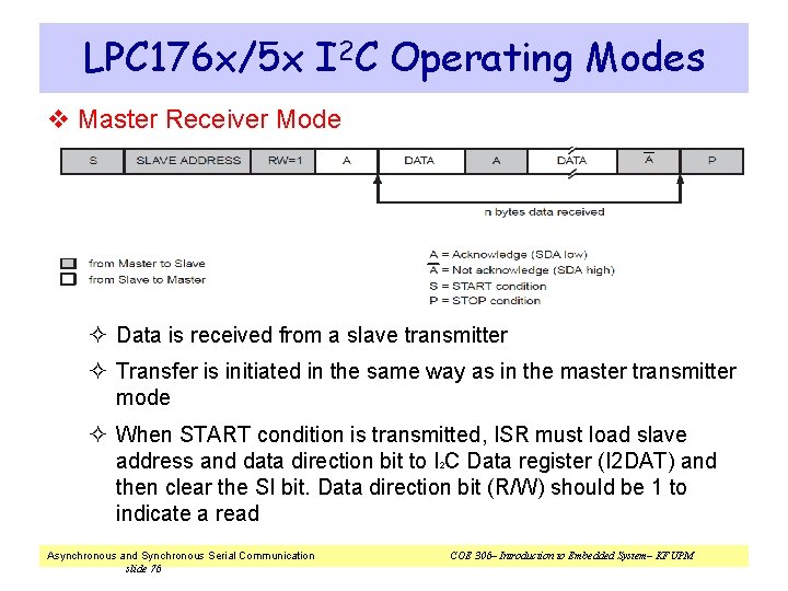
LPC 176 x/5 x I 2 C Operating Modes v Master Receiver Mode ² Data is received from a slave transmitter ² Transfer is initiated in the same way as in the master transmitter mode ² When START condition is transmitted, ISR must load slave address and data direction bit to I C Data register (I 2 DAT) and then clear the SI bit. Data direction bit (R/W) should be 1 to indicate a read 2 Asynchronous and Synchronous Serial Communication slide 76 COE 306– Introduction to Embedded System– KFUPM

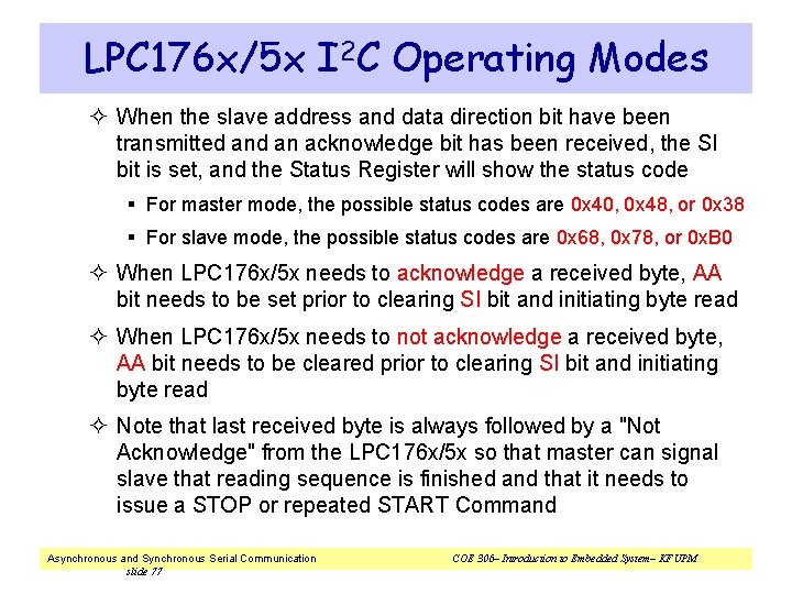
LPC 176 x/5 x I 2 C Operating Modes ² When the slave address and data direction bit have been transmitted an acknowledge bit has been received, the SI bit is set, and the Status Register will show the status code § For master mode, the possible status codes are 0 x 40, 0 x 48, or 0 x 38 § For slave mode, the possible status codes are 0 x 68, 0 x 78, or 0 x. B 0 ² When LPC 176 x/5 x needs to acknowledge a received byte, AA bit needs to be set prior to clearing SI bit and initiating byte read ² When LPC 176 x/5 x needs to not acknowledge a received byte, AA bit needs to be cleared prior to clearing SI bit and initiating byte read ² Note that last received byte is always followed by a "Not Acknowledge" from the LPC 176 x/5 x so that master can signal slave that reading sequence is finished and that it needs to issue a STOP or repeated START Command Asynchronous and Synchronous Serial Communication slide 77 COE 306– Introduction to Embedded System– KFUPM

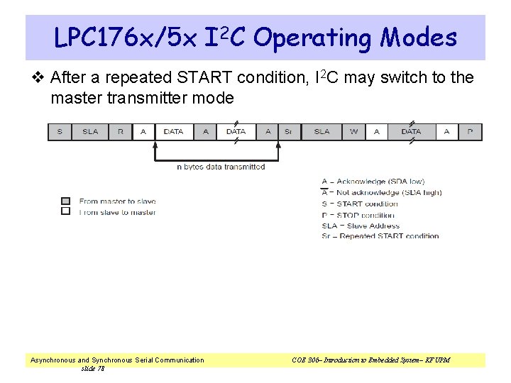
LPC 176 x/5 x I 2 C Operating Modes v After a repeated START condition, I 2 C may switch to the master transmitter mode Asynchronous and Synchronous Serial Communication slide 78 COE 306– Introduction to Embedded System– KFUPM

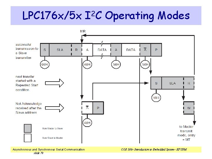
LPC 176 x/5 x I 2 C Operating Modes Asynchronous and Synchronous Serial Communication slide 79 COE 306– Introduction to Embedded System– KFUPM

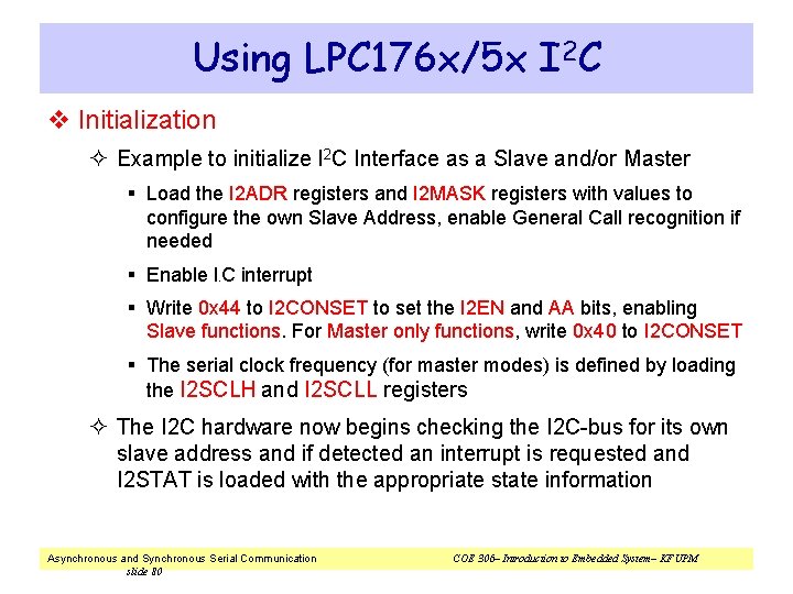
Using LPC 176 x/5 x I 2 C v Initialization ² Example to initialize I 2 C Interface as a Slave and/or Master § Load the I 2 ADR registers and I 2 MASK registers with values to configure the own Slave Address, enable General Call recognition if needed § Enable I C interrupt 2 § Write 0 x 44 to I 2 CONSET to set the I 2 EN and AA bits, enabling Slave functions. For Master only functions, write 0 x 40 to I 2 CONSET § The serial clock frequency (for master modes) is defined by loading the I 2 SCLH and I 2 SCLL registers ² The I 2 C hardware now begins checking the I 2 C-bus for its own slave address and if detected an interrupt is requested and I 2 STAT is loaded with the appropriate state information Asynchronous and Synchronous Serial Communication slide 80 COE 306– Introduction to Embedded System– KFUPM

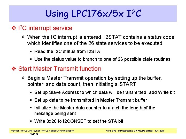
Using LPC 176 x/5 x I 2 C v I 2 C interrupt service ² When the I C interrupt is entered, I 2 STAT contains a status code which identifies one of the 26 state services to be executed 2 § Read the I 2 C status from I 2 STA § Use the status value to branch to one of 26 possible state routines v Start Master Transmit function ² Begin a Master Transmit operation by setting up the buffer, pointer, and data count, then initiating a START § Set up Slave Address to which data will be transmitted, add Write bit § Set up data to be transmitted in Master Transmit buffer § Initialize the Master data counter to match the length of the message being sent § Write 0 x 20 to I 2 CONSET to set the STA bit Asynchronous and Synchronous Serial Communication slide 81 COE 306– Introduction to Embedded System– KFUPM

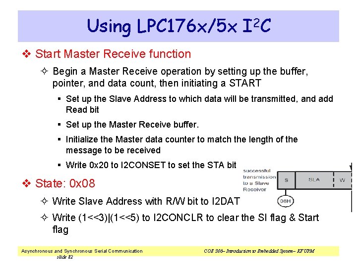
Using LPC 176 x/5 x I 2 C v Start Master Receive function ² Begin a Master Receive operation by setting up the buffer, pointer, and data count, then initiating a START § Set up the Slave Address to which data will be transmitted, and add Read bit § Set up the Master Receive buffer. § Initialize the Master data counter to match the length of the message to be received § Write 0 x 20 to I 2 CONSET to set the STA bit v State: 0 x 08 ² Write Slave Address with R/W bit to I 2 DAT ² Write (1<<3)|(1<<5) to I 2 CONCLR to clear the SI flag & Start flag Asynchronous and Synchronous Serial Communication slide 82 COE 306– Introduction to Embedded System– KFUPM

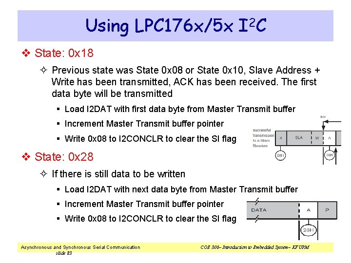
Using LPC 176 x/5 x I 2 C v State: 0 x 18 ² Previous state was State 0 x 08 or State 0 x 10, Slave Address + Write has been transmitted, ACK has been received. The first data byte will be transmitted § Load I 2 DAT with first data byte from Master Transmit buffer § Increment Master Transmit buffer pointer § Write 0 x 08 to I 2 CONCLR to clear the SI flag v State: 0 x 28 ² If there is still data to be written § Load I 2 DAT with next data byte from Master Transmit buffer § Increment Master Transmit buffer pointer § Write 0 x 08 to I 2 CONCLR to clear the SI flag Asynchronous and Synchronous Serial Communication slide 83 COE 306– Introduction to Embedded System– KFUPM

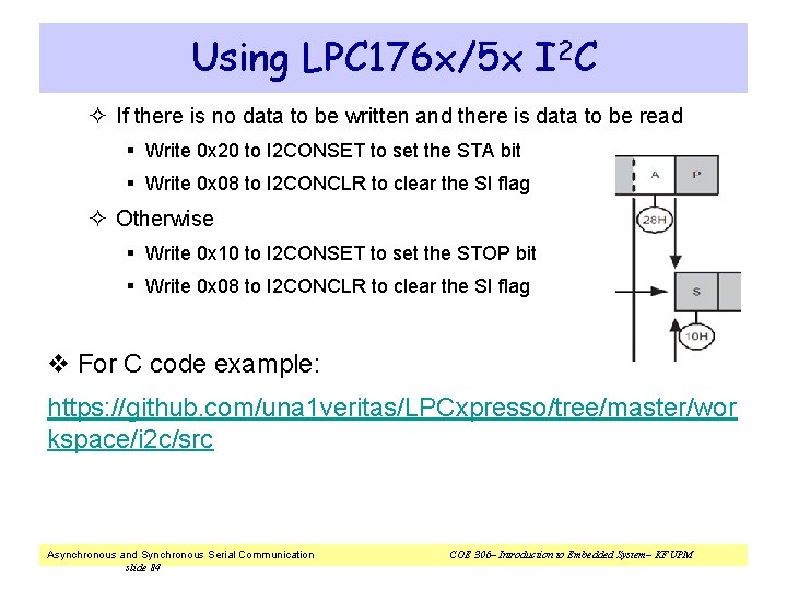
Using LPC 176 x/5 x I 2 C ² If there is no data to be written and there is data to be read § Write 0 x 20 to I 2 CONSET to set the STA bit § Write 0 x 08 to I 2 CONCLR to clear the SI flag ² Otherwise § Write 0 x 10 to I 2 CONSET to set the STOP bit § Write 0 x 08 to I 2 CONCLR to clear the SI flag v For C code example: https: //github. com/una 1 veritas/LPCxpresso/tree/master/wor kspace/i 2 c/src Asynchronous and Synchronous Serial Communication slide 84 COE 306– Introduction to Embedded System– KFUPM

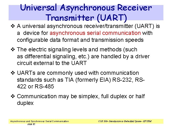
Universal Asynchronous Receiver Transmitter (UART) v A universal asynchronous receiver/transmitter (UART) is a device for asynchronous serial communication with configurable data format and transmission speeds v The electric signaling levels and methods (such as differential signaling, etc. ) are handled by a driver circuit external to the UART v UARTs are commonly used with communication standards such as TIA (formerly EIA) RS-232, RS 422 or RS-485 v Communication may be simplex, full duplex or half duplex Asynchronous and Synchronous Serial Communication slide 85 COE 306– Introduction to Embedded System– KFUPM

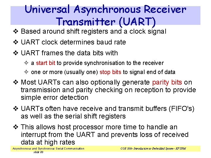
Universal Asynchronous Receiver Transmitter (UART) v Based around shift registers and a clock signal v UART clock determines baud rate v UART frames the data bits with ² a start bit to provide synchronisation to the receiver ² one or more (usually one) stop bits to signal end of data v Most UARTs can also optionally generate parity bits on transmission and parity checking on reception to provide simple error detection v UARTs often have receive and transmit buffers (FIFO's) as well as the serial shift registers v This allows host processor more time to handle an interrupt from the UART and prevents loss of received data at high rates Asynchronous and Synchronous Serial Communication slide 86 COE 306– Introduction to Embedded System– KFUPM

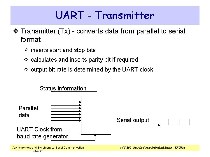
UART - Transmitter v Transmitter (Tx) - converts data from parallel to serial format ² inserts start and stop bits ² calculates and inserts parity bit if required ² output bit rate is determined by the UART clock Status information Parallel data Serial output UART Clock from baud rate generator Asynchronous and Synchronous Serial Communication slide 87 COE 306– Introduction to Embedded System– KFUPM

Asynchronous Serial Transmission 1 0 Serial transmission is little endian (least significant bit first) Asynchronous and Synchronous Serial Communication slide 88 COE 306– Introduction to Embedded System– KFUPM

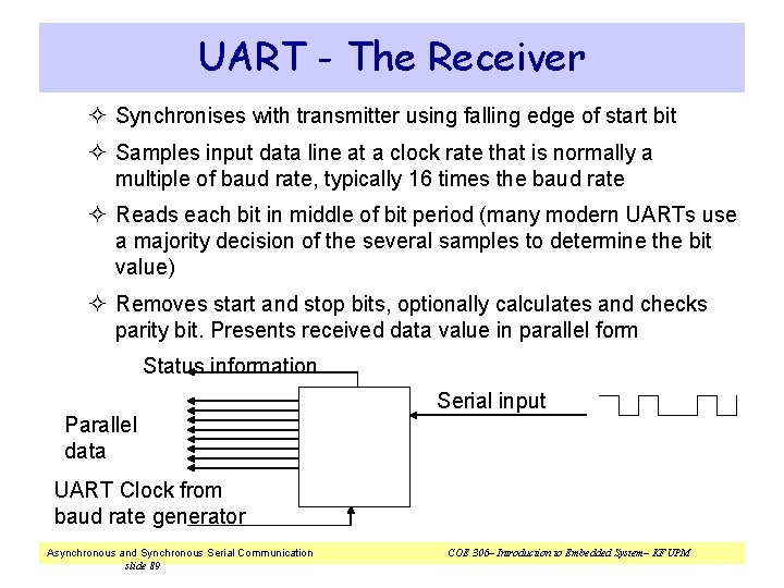
UART - The Receiver ² Synchronises with transmitter using falling edge of start bit ² Samples input data line at a clock rate that is normally a multiple of baud rate, typically 16 times the baud rate ² Reads each bit in middle of bit period (many modern UARTs use a majority decision of the several samples to determine the bit value) ² Removes start and stop bits, optionally calculates and checks parity bit. Presents received data value in parallel form Status information Serial input Parallel data UART Clock from baud rate generator Asynchronous and Synchronous Serial Communication slide 89 COE 306– Introduction to Embedded System– KFUPM

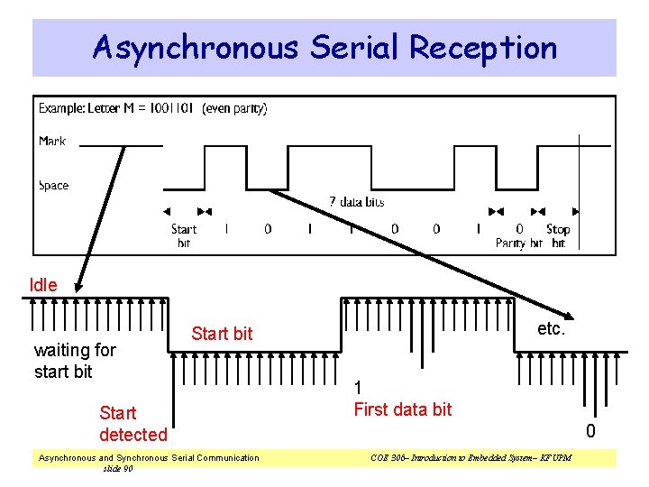
Asynchronous Serial Reception Idle waiting for start bit etc. Start bit Start detected Asynchronous and Synchronous Serial Communication slide 90 1 First data bit 0 COE 306– Introduction to Embedded System– KFUPM

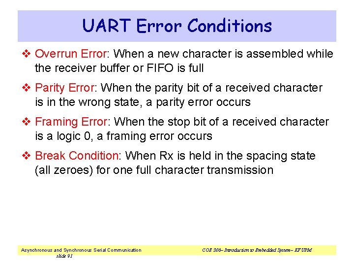
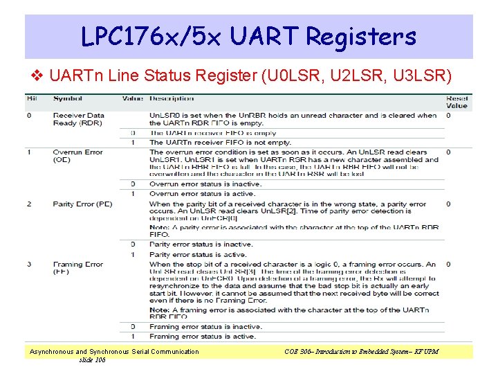
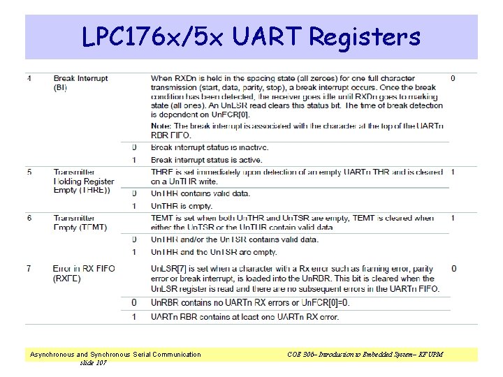
UART Error Conditions v Overrun Error: When a new character is assembled while the receiver buffer or FIFO is full v Parity Error: When the parity bit of a received character is in the wrong state, a parity error occurs v Framing Error: When the stop bit of a received character is a logic 0, a framing error occurs v Break Condition: When Rx is held in the spacing state (all zeroes) for one full character transmission Asynchronous and Synchronous Serial Communication slide 91 COE 306– Introduction to Embedded System– KFUPM

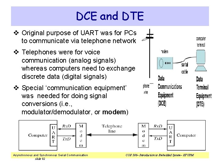
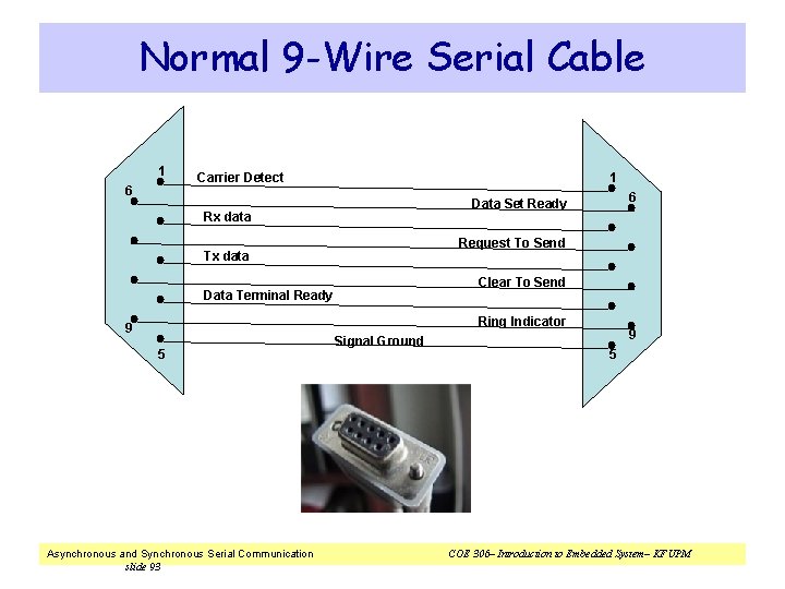
DCE and DTE v Original purpose of UART was for PCs to communicate via telephone network v Telephones were for voice communication (analog signals) whereas computers need to exchange discrete data (digital signals) v Special ‘communication equipment’ was needed for doing signal conversions (i. e. , modulator/demodulator, or modem) Asynchronous and Synchronous Serial Communication slide 92 COE 306– Introduction to Embedded System– KFUPM

Normal 9 -Wire Serial Cable 1 6 Carrier Detect 1 6 Data Set Ready Rx data Request To Send Tx data Clear To Send Data Terminal Ready Ring Indicator 9 5 Asynchronous and Synchronous Serial Communication slide 93 Signal Ground 9 5 COE 306– Introduction to Embedded System– KFUPM

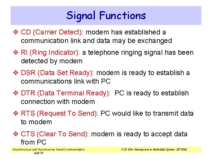
Signal Functions v CD (Carrier Detect): modem has established a communication link and data may be exchanged v RI (Ring Indicator): a telephone ringing signal has been detected by modem v DSR (Data Set Ready): modem is ready to establish a communications link with PC v DTR (Data Terminal Ready): PC is ready to establish connection with modem v RTS (Request To Send): PC would like to transmit data to modem v CTS (Clear To Send): modem is ready to accept data from PC Asynchronous and Synchronous Serial Communication slide 94 COE 306– Introduction to Embedded System– KFUPM

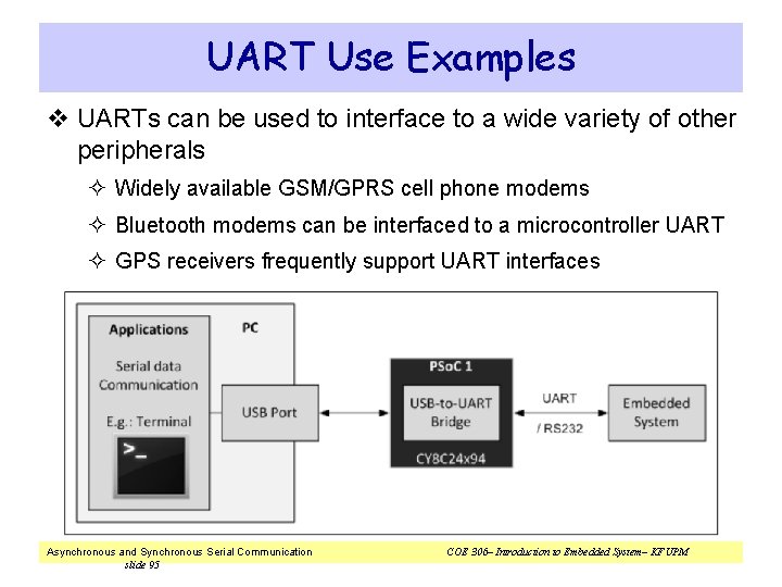
UART Use Examples v UARTs can be used to interface to a wide variety of other peripherals ² Widely available GSM/GPRS cell phone modems ² Bluetooth modems can be interfaced to a microcontroller UART ² GPS receivers frequently support UART interfaces Asynchronous and Synchronous Serial Communication slide 95 COE 306– Introduction to Embedded System– KFUPM

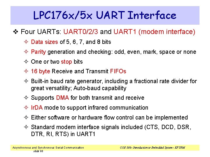
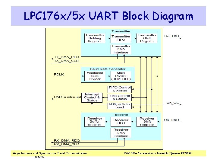
LPC 176 x/5 x UART Interface v Four UARTs: UART 0/2/3 and UART 1 (modem interface) ² Data sizes of 5, 6, 7, and 8 bits ² Parity generation and checking: odd, even, mark, space or none ² One or two stop bits ² 16 byte Receive and Transmit FIFOs ² Built-in baud rate generator, including a fractional rate divider for great versatility; Auto-baud capability ² Supports DMA for both transmit and receive ² Ir. DA mode to support infrared communication ² Either software or hardware flow control can be implemented ² Standard modem interface signals included (CTS, DCD, DSR, DTR, RI, RTS) in UART 1 Asynchronous and Synchronous Serial Communication slide 96 COE 306– Introduction to Embedded System– KFUPM

LPC 176 x/5 x UART Block Diagram Asynchronous and Synchronous Serial Communication slide 97 COE 306– Introduction to Embedded System– KFUPM

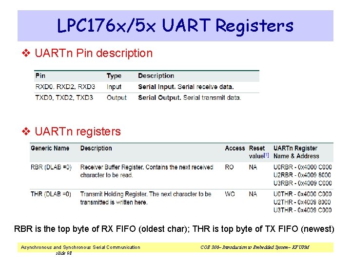
LPC 176 x/5 x UART Registers v UARTn Pin description v UARTn registers RBR is the top byte of RX FIFO (oldest char); THR is top byte of TX FIFO (newest) Asynchronous and Synchronous Serial Communication slide 98 COE 306– Introduction to Embedded System– KFUPM

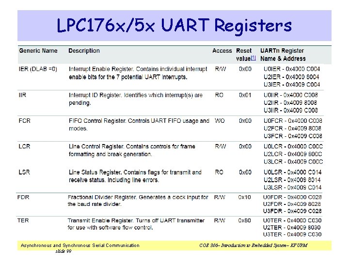
LPC 176 x/5 x UART Registers Asynchronous and Synchronous Serial Communication slide 99 COE 306– Introduction to Embedded System– KFUPM

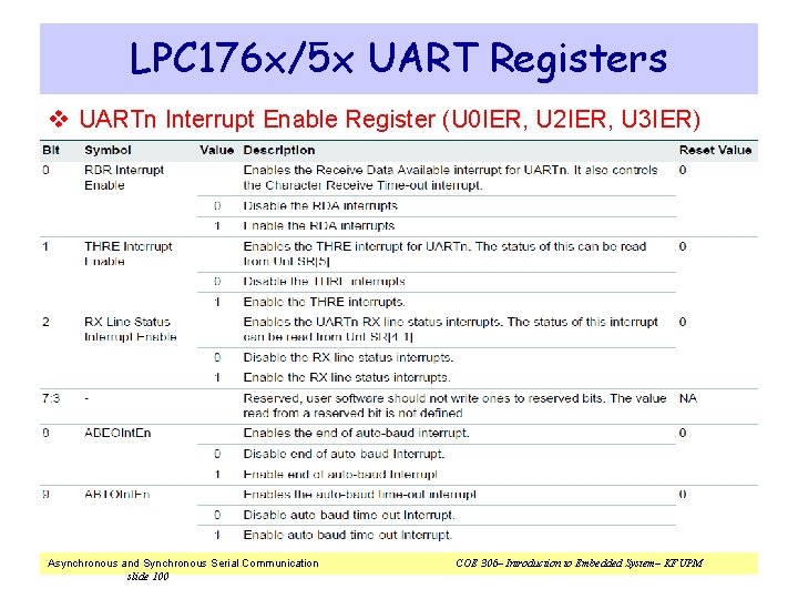
LPC 176 x/5 x UART Registers v UARTn Interrupt Enable Register (U 0 IER, U 2 IER, U 3 IER) Asynchronous and Synchronous Serial Communication slide 100 COE 306– Introduction to Embedded System– KFUPM

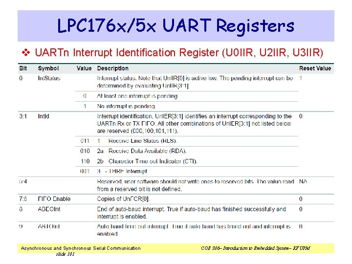
LPC 176 x/5 x UART Registers v UARTn Interrupt Identification Register (U 0 IIR, U 2 IIR, U 3 IIR) Asynchronous and Synchronous Serial Communication slide 101 COE 306– Introduction to Embedded System– KFUPM
![LPC 176 x5 x UART Registers v The UARTn RLS interrupt Un IIR3 1 LPC 176 x/5 x UART Registers v The UARTn RLS interrupt (Un. IIR[3: 1]](https://slidetodoc.com/presentation_image_h/ce8e085b4b9e5442b3ce9c406af3e9c1/image-102.jpg)
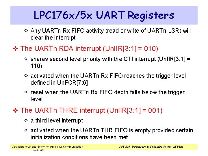
LPC 176 x/5 x UART Registers v The UARTn RLS interrupt (Un. IIR[3: 1] = 011) ² highest priority interrupt ² set whenever any one of four error conditions occur on UARTn Rx input: overrun error (OE), parity error (PE), framing error (FE) and break interrupt (BI) ² UARTn Rx error condition that sets the interrupt can be observed via Un. LSR[4: 1] ² The interrupt is cleared upon an Un. LSR read v The CTI interrupt (Un. IIR[3: 1] = 110) ² a second level interrupt ² set when the UARTn Rx FIFO contains at least one character and no UARTn Rx FIFO activity has occurred in 3. 5 to 4. 5 character times Asynchronous and Synchronous Serial Communication slide 102 COE 306– Introduction to Embedded System– KFUPM

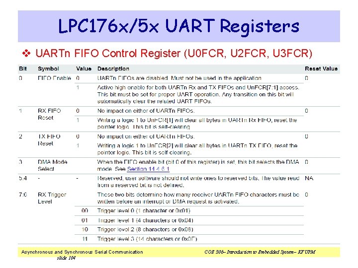
LPC 176 x/5 x UART Registers ² Any UARTn Rx FIFO activity (read or write of UARTn LSR) will clear the interrupt v The UARTn RDA interrupt (Un. IIR[3: 1] = 010) ² shares second level priority with the CTI interrupt (Un. IIR[3: 1] = 110) ² activated when the UARTn Rx FIFO reaches the trigger level defined in Un. FCR[7: 6] ² reset when the UARTn Rx FIFO depth falls below the trigger level v The UARTn THRE interrupt (Un. IIR[3: 1] = 001) ² a third level interrupt ² activated when the UARTn THR FIFO is empty provided certain initialization conditions have been met Asynchronous and Synchronous Serial Communication slide 103 COE 306– Introduction to Embedded System– KFUPM

LPC 176 x/5 x UART Registers v UARTn FIFO Control Register (U 0 FCR, U 2 FCR, U 3 FCR) Asynchronous and Synchronous Serial Communication slide 104 COE 306– Introduction to Embedded System– KFUPM

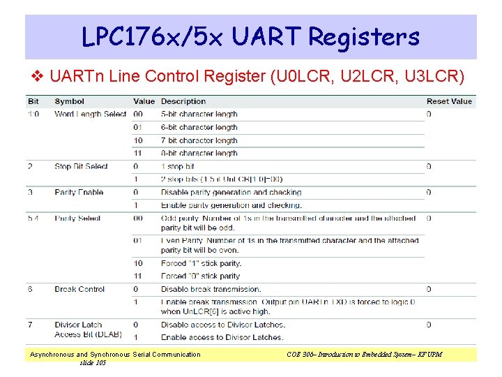
LPC 176 x/5 x UART Registers v UARTn Line Control Register (U 0 LCR, U 2 LCR, U 3 LCR) Asynchronous and Synchronous Serial Communication slide 105 COE 306– Introduction to Embedded System– KFUPM

LPC 176 x/5 x UART Registers v UARTn Line Status Register (U 0 LSR, U 2 LSR, U 3 LSR) Asynchronous and Synchronous Serial Communication slide 106 COE 306– Introduction to Embedded System– KFUPM

LPC 176 x/5 x UART Registers Asynchronous and Synchronous Serial Communication slide 107 COE 306– Introduction to Embedded System– KFUPM

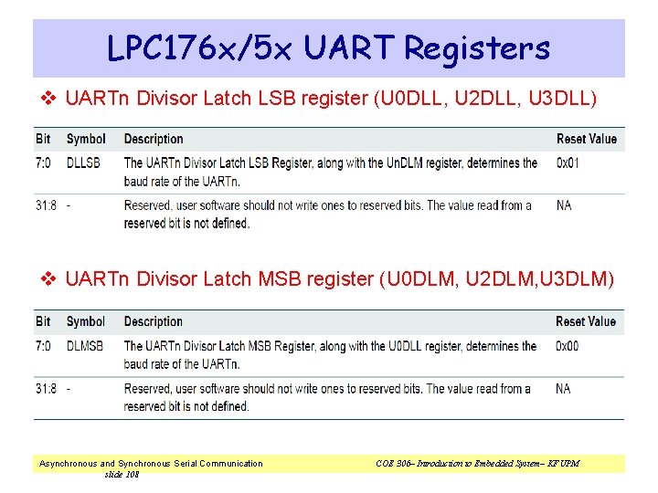
LPC 176 x/5 x UART Registers v UARTn Divisor Latch LSB register (U 0 DLL, U 2 DLL, U 3 DLL) v UARTn Divisor Latch MSB register (U 0 DLM, U 2 DLM, U 3 DLM) Asynchronous and Synchronous Serial Communication slide 108 COE 306– Introduction to Embedded System– KFUPM

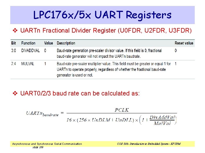
LPC 176 x/5 x UART Registers v UARTn Fractional Divider Register (U 0 FDR, U 2 FDR, U 3 FDR) v UART 0/2/3 baud rate can be calculated as: Asynchronous and Synchronous Serial Communication slide 109 COE 306– Introduction to Embedded System– KFUPM

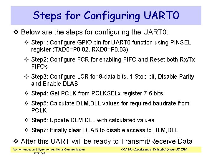
Steps for Configuring UART 0 v Below are the steps for configuring the UART 0: ² Step 1: Configure GPIO pin for UART 0 function using PINSEL register (TXD 0=P 0. 02, RXD 0=P 0. 03) ² Step 2: Configure FCR for enabling FIFO and Reset both Rx/Tx FIFOs ² Step 3: Configure LCR for 8 -data bits, 1 Stop bit, Disable Parity and Enable DLAB ² Step 4: Get PCLK from PCLKSELx register 7 -6 bits ² Step 5: Calculate DLM, DLL values for required baudrate from PCLK ² Step 6: Update DLM, DLL with calculated values ² Step 7: Finally clear DLAB to disable access to DLM, DLL v After this UART will be ready to Transmit/Receive Data Asynchronous and Synchronous Serial Communication slide 110 COE 306– Introduction to Embedded System– KFUPM

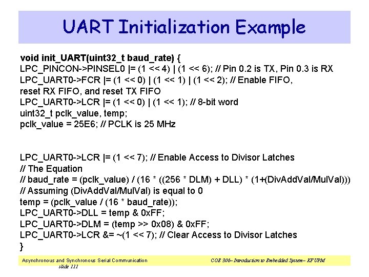
UART Initialization Example void init_UART(uint 32_t baud_rate) { LPC_PINCON->PINSEL 0 |= (1 << 4) | (1 << 6); // Pin 0. 2 is TX, Pin 0. 3 is RX LPC_UART 0 ->FCR |= (1 << 0) | (1 << 1) | (1 << 2); // Enable FIFO, reset RX FIFO, and reset TX FIFO LPC_UART 0 ->LCR |= (1 << 0) | (1 << 1); // 8 -bit word uint 32_t pclk_value, temp; pclk_value = 25 E 6; // PCLK is 25 MHz LPC_UART 0 ->LCR |= (1 << 7); // Enable Access to Divisor Latches // The Equation // baud_rate = (pclk_value) / (16 * ((256 * DLM) + DLL) * (1+(Div. Add. Val/Mul. Val))) // Assuming (Div. Add. Val/Mul. Val) is equal to 0 temp = (pclk_value / (16 * baud_rate)); LPC_UART 0 ->DLL = temp & 0 x. FF; LPC_UART 0 ->DLM = (temp >> 0 x 08) & 0 x. FF; LPC_UART 0 ->LCR &= ~(1 << 7); // Clear Access to Divisor Latches } Asynchronous and Synchronous Serial Communication slide 111 COE 306– Introduction to Embedded System– KFUPM

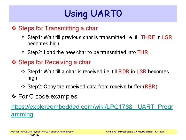
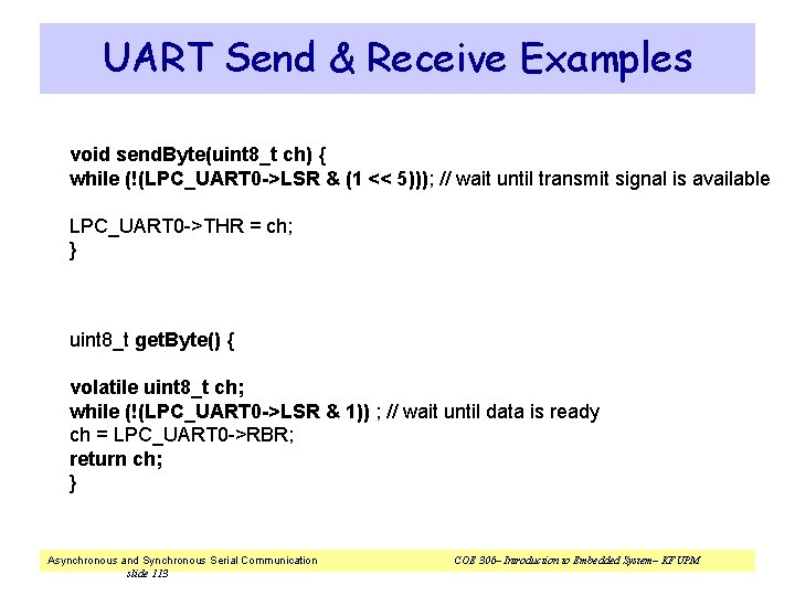
Using UART 0 v Steps for Transmitting a char ² Step 1: Wait till previous char is transmitted i. e. till THRE in LSR becomes high ² Step 2: Load the new char to be transmitted into THR v Steps for Receiving a char ² Step 1: Wait till a char is received i. e. till RDR in LSR becomes high ² Step 2: Copy the received data from receive buffer (RBR) v For C code examples: https: //exploreembedded. com/wiki/LPC 1768: _UART_Progr amming Asynchronous and Synchronous Serial Communication slide 112 COE 306– Introduction to Embedded System– KFUPM

UART Send & Receive Examples void send. Byte(uint 8_t ch) { while (!(LPC_UART 0 ->LSR & (1 << 5))); // wait until transmit signal is available LPC_UART 0 ->THR = ch; } uint 8_t get. Byte() { volatile uint 8_t ch; while (!(LPC_UART 0 ->LSR & 1)) ; // wait until data is ready ch = LPC_UART 0 ->RBR; return ch; } Asynchronous and Synchronous Serial Communication slide 113 COE 306– Introduction to Embedded System– KFUPM