ASIC Implementation of LDPC Decoder Accelerating MessagePassing Schedule
- Slides: 3

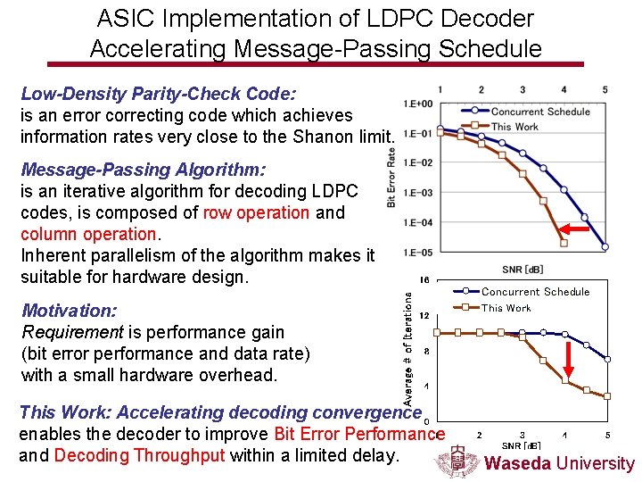
ASIC Implementation of LDPC Decoder Accelerating Message-Passing Schedule Low-Density Parity-Check Code: is an error correcting code which achieves information rates very close to the Shanon limit. Message-Passing Algorithm: is an iterative algorithm for decoding LDPC codes, is composed of row operation and column operation. Inherent parallelism of the algorithm makes it suitable for hardware design. Motivation: Requirement is performance gain (bit error performance and data rate) with a small hardware overhead. This Work: Accelerating decoding convergence enables the decoder to improve Bit Error Performance and Decoding Throughput within a limited delay. Waseda University

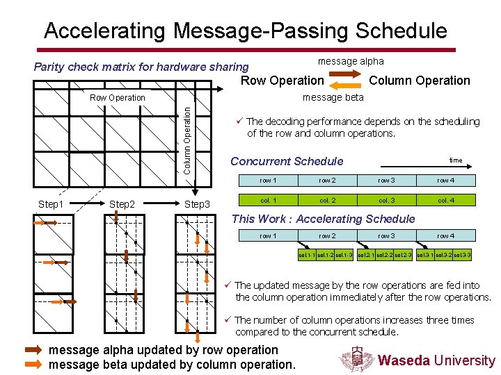
Accelerating Message-Passing Schedule message alpha Parity check matrix for hardware sharing Row Operation message beta Column Operation Row Operation Step 1 Step 2 Column Operation Step 3 ü The decoding performance depends on the scheduling of the row and column operations. Concurrent Schedule time row 1 row 2 row 3 row 4 col. 1 col. 2 col. 3 col. 4 This Work : Accelerating Schedule row 1 row 2 col. 1 -1 col. 1 -2 col. 1 -3 row 3 col. 2 -1 col. 2 -2 col. 2 -3 row 4 col. 3 -1 col. 3 -2 col. 3 -3 ü The updated message by the row operations are fed into the column operation immediately after the row operations. ü The number of column operations increases three times compared to the concurrent schedule. message alpha updated by row operation message beta updated by column operation. Waseda University

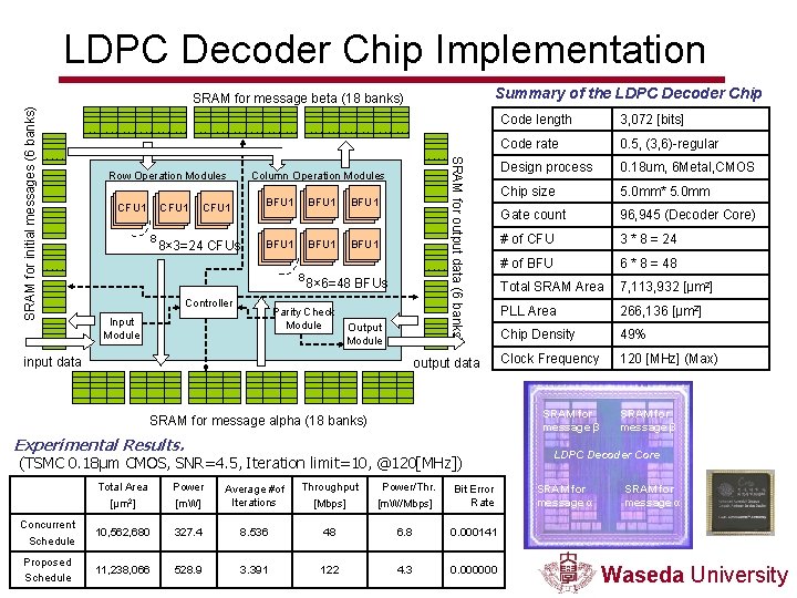
LDPC Decoder Chip Implementation Summary of the LDPC Decoder Chip . . . . . Row Operation Modules . . CFU 1 . . 8 Column Operation Modules BFU 1 CFU 1 BFU 1 . . 8× 3=24 CFUs BFU 1 . . BFU 1 8 . . Controller BFU 1 . . 8× 6=48 BFUs Parity Check Module Input Module . . . . BFU 1 . . Output Module . . input data SRAM for output data (6 banks) SRAM for initial messages (6 banks) SRAM for message beta (18 banks) output data Code length 3, 072 [bits] Code rate 0. 5, (3, 6)-regular Design process 0. 18 um, 6 Metal, CMOS Chip size 5. 0 mm* 5. 0 mm Gate count 96, 945 (Decoder Core) # of CFU 3 * 8 = 24 # of BFU 6 * 8 = 48 Total SRAM Area 7, 113, 932 [μm 2] PLL Area 266, 136 [μm 2] Chip Density 49% Clock Frequency 120 [MHz] (Max) . . . . SRAM for message β SRAM for message alpha (18 banks) Experimental Results. (TSMC 0. 18μm CMOS, SNR=4. 5, Iteration limit=10, @120[MHz]) Total Area [μm 2] Power [m. W] Average #of Iterations Throughput [Mbps] Power/Thr. [m. W/Mbps] Bit Error Rate Concurrent Schedule 10, 562, 680 327. 4 8. 536 48 6. 8 0. 000141 Proposed Schedule 11, 238, 066 528. 9 3. 391 122 4. 3 0. 000000 SRAM for message β LDPC Decoder Core SRAM for message α Waseda University