ASIC Electronics development for CDEX PCGe detector Xuezhou

- Slides: 19

ASIC Electronics development for CDEX PCGe detector Xuezhou Zhu, Zhi Deng Department of Engineering Physics, Tsinghua University 14/10/2013核电子学ASIC技术研讨会

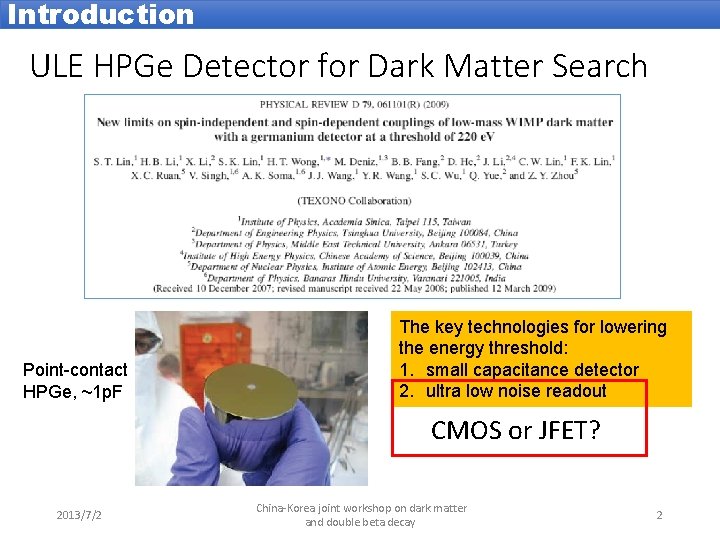
Introduction ULE HPGe Detector for Dark Matter Search Point-contact HPGe, ~1 p. F The key technologies for lowering the energy threshold: 1. small capacitance detector 2. ultra low noise readout CMOS or JFET? 2013/7/2 China-Korea joint workshop on dark matter and double beta decay 2

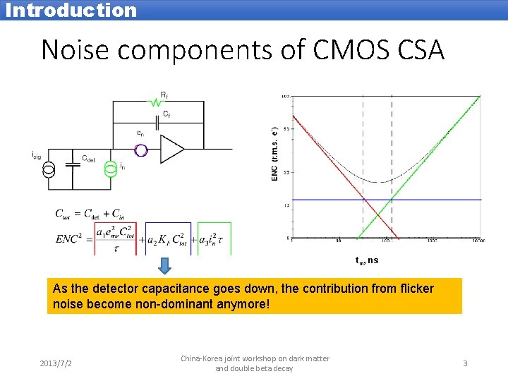
Introduction Noise components of CMOS CSA tm, ns As the detector capacitance goes down, the contribution from flicker noise become non-dominant anymore! 2013/7/2 China-Korea joint workshop on dark matter and double beta decay 3

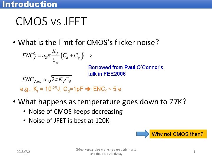
Introduction CMOS vs JFET • What is the limit for CMOS’s flicker noise? Borrowed from Paul O’Connor’s talk in FEE 2006 e. g. , Kf = 10 -25 J, Cd=1 p. F ENCf ~ 5 e- • What happens as temperature goes down to 77 K? • Noise of CMOS keeps decreasing • Noise of JFET is best at 120 K Why not CMOS then? 2013/7/2 China-Korea joint workshop on dark matter and double beta decay 4

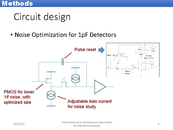
Methods Circuit design • Noise Optimization for 1 p. F Detectors Pulse reset PMOS for lower 1/f noise, with optimized size 2013/7/2 Adjustable bias current for noise study China-Korea joint workshop on dark matter and double beta decay 5

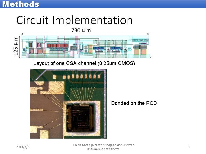
Methods Circuit Implementation Layout of one CSA channel (0. 35 um CMOS) Bonded on the PCB 2013/7/2 China-Korea joint workshop on dark matter and double beta decay 6

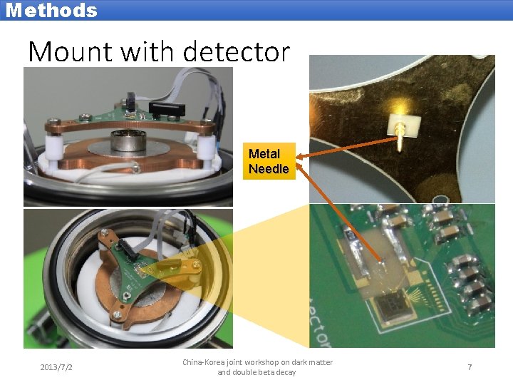
Methods Mount with detector Metal Needle 2013/7/2 China-Korea joint workshop on dark matter and double beta decay 7

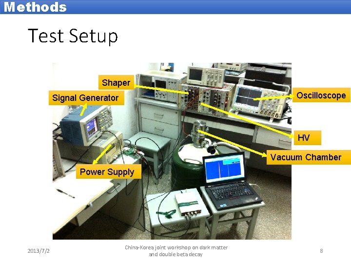
Methods Test Setup Shaper Oscilloscope Signal Generator HV Vacuum Chamber Power Supply 2013/7/2 China-Korea joint workshop on dark matter and double beta decay 8

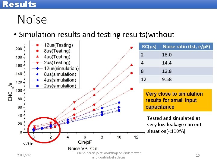
Results Noise • Simulation results and testing results(without detector) Very close to simulation results for small input capacitance Tested and simulated at very low leakage current situation(<100 f. A) <20 e 2013/7/2 China-Korea joint workshop on dark matter and double beta decay 10

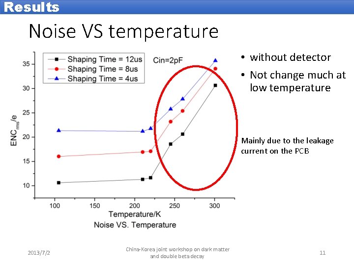
Results Noise VS temperature • without detector • Not change much at low temperature Mainly due to the leakage current on the PCB 2013/7/2 China-Korea joint workshop on dark matter and double beta decay 11

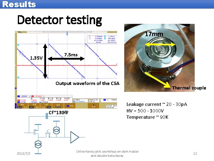
Results Detector testing 17 mm 1. 35 V 7. 5 ms Output waveform of the CSA Cf~130 f. F 2013/7/2 Thermal couple Leakage current ~ 20 - 30 p. A HV = 500 - 1000 V Temperature ~ 90 K China-Korea joint workshop on dark matter and double beta decay 12

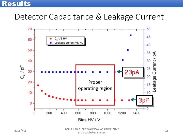
Results Detector Capacitance & Leakage Current 23 p. A Properating region 3 p. F 2013/7/2 China-Korea joint workshop on dark matter and double beta decay 13

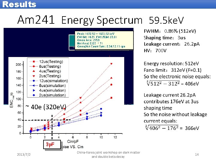
Results Am 241 Energy Spectrum 59. 5 ke. V FWHM: 0. 86% (512 e. V) Shaping time: 3 us Leakage current: 26. 2 p. A HV: 700 V ~ 40 e (320 e. V) 3 p. F 2013/7/2 China-Korea joint workshop on dark matter and double beta decay 14

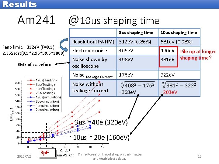
Results Am 241 @10 us shaping time 3 us shaping time Fano limit: 312 e. V (F=0. 1) 2. 355 sqrt(0. 1*2. 96*59. 5*1000) RMS of waveform 10 us shaping time Resolution(FWHM) 512 e. V (0. 86%) 581 e. V (0. 98%) Electronic noise 406 e. V Noise shown by oscilloscope 408 e. V 490 e. V Pile up at longer 381 e. V shaping time? Noise Leakage Current 176 e. V 322 e. V Noise without Leakage Current 3 us ~ 40 e (320 e. V) 10 us ~ 20 e (160 e. V) 2013/7/2 3 p. F China-Korea joint workshop on dark matter and double beta decay 15

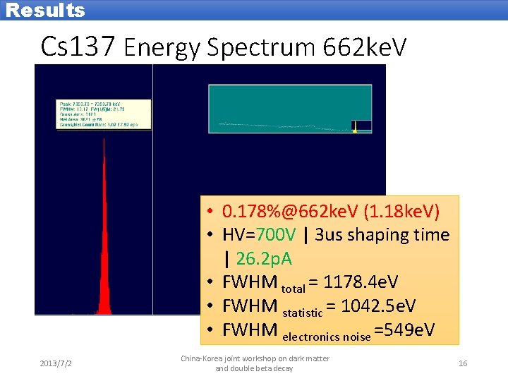
Results Cs 137 Energy Spectrum 662 ke. V • 0. 178%@662 ke. V (1. 18 ke. V) • HV=700 V | 3 us shaping time | 26. 2 p. A • FWHM total = 1178. 4 e. V • FWHM statistic = 1042. 5 e. V • FWHM electronics noise =549 e. V 2013/7/2 China-Korea joint workshop on dark matter and double beta decay 16

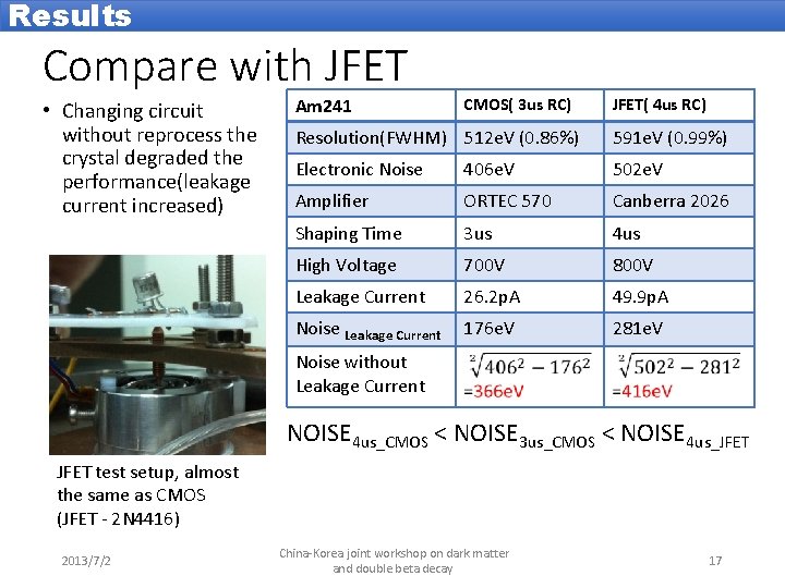
Results Compare with JFET • Changing circuit without reprocess the crystal degraded the performance(leakage current increased) Am 241 CMOS( 3 us RC) JFET( 4 us RC) Resolution(FWHM) 512 e. V (0. 86%) 591 e. V (0. 99%) Electronic Noise 406 e. V 502 e. V Amplifier ORTEC 570 Canberra 2026 Shaping Time 3 us 4 us High Voltage 700 V 800 V Leakage Current 26. 2 p. A 49. 9 p. A Noise Leakage Current 176 e. V 281 e. V Noise without Leakage Current NOISE 4 us_CMOS < NOISE 3 us_CMOS < NOISE 4 us_JFET test setup, almost the same as CMOS (JFET - 2 N 4416) 2013/7/2 China-Korea joint workshop on dark matter and double beta decay 17

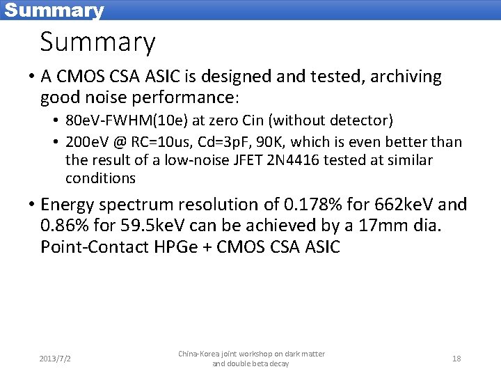
Summary • A CMOS CSA ASIC is designed and tested, archiving good noise performance: • 80 e. V-FWHM(10 e) at zero Cin (without detector) • 200 e. V @ RC=10 us, Cd=3 p. F, 90 K, which is even better than the result of a low-noise JFET 2 N 4416 tested at similar conditions • Energy spectrum resolution of 0. 178% for 662 ke. V and 0. 86% for 59. 5 ke. V can be achieved by a 17 mm dia. Point-Contact HPGe + CMOS CSA ASIC 2013/7/2 China-Korea joint workshop on dark matter and double beta decay 18

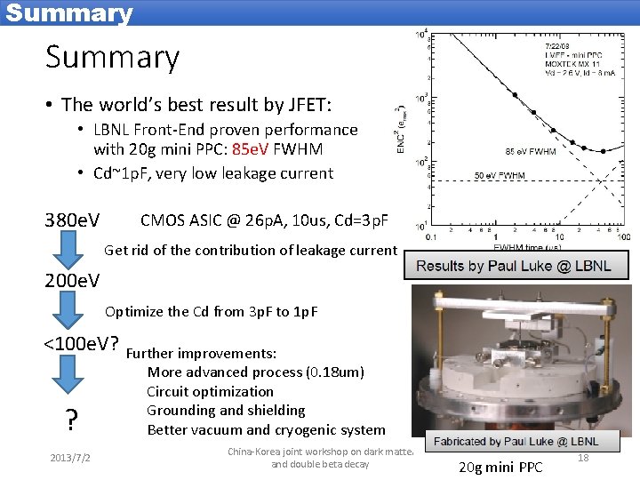
Summary • The world’s best result by JFET: • LBNL Front-End proven performance with 20 g mini PPC: 85 e. V FWHM • Cd~1 p. F, very low leakage current 380 e. V CMOS ASIC @ 26 p. A, 10 us, Cd=3 p. F Get rid of the contribution of leakage current 200 e. V Optimize the Cd from 3 p. F to 1 p. F <100 e. V? Further improvements: ? 2013/7/2 More advanced process (0. 18 um) Circuit optimization Grounding and shielding Better vacuum and cryogenic system China-Korea joint workshop on dark matter and double beta decay 20 g mini PPC 18

Summary Thank you • Q&A