ASIC Application specific integrated circuit CS 2630 Computer


 Note")


- Slides: 39
ASIC = “Application specific integrated circuit”
CS 2630 Computer Organization Meeting 19: Building a MIPS processor Brandon Myers University of Iowa
The goal: implement most of MIPS
So far
Implementing the addu instruction register file
still need to: • support more than 1 kind of arithmetic operation • feed the CPU with a program • support branches and load/store
Next: we’ve discussed what is in this box, but we need to learn about the rest of what is needed for a MIPS processor Project 2 -1: the stuff in this box Project 2 -2: everything else
Implementing the addu instruction register file How do we program the “addu machine”?
Peer instruction Give the sequence of addu machine inputs to perform $t 0 = $t 1 + $t 2 + $t 3 a) 1 st clock cycle: rd=8, rs=9, rt=10 2 nd clock cycle: rd=8, rs=8, rt=11 b) 1 st clock cycle: rd=0, rs=9, rt=10 2 nd clock cycle: rd=8, rs=0, rt=0 3 rd clock cycle: rd=0, rs=8, rt=11 4 th clock cycle: rd=8, rs=0, rt=0 c) 1 st clock cycle: rd=0, rs=10, rt=11 2 nd clock cycle: rd=8, rs=0, rt=0 3 rd clock cycle: rd=0, rs=8, rt=9 4 th clock cycle: rd=8, rs=0, rt=0 d) 1 st clock cycle: rd=9, rs=10, rt=11 2 nd clock cycle: rd=8, rs=0, rt=0
How do we program the addu machine? • Example: 8 8 14 On each clock cycle, we are allowed to change the inputs rd, rs, and rt to perform another addition.
But, where do those inputs come from?
mining difficulty year “the difficulty target is adjusted based on the network's recent performance, with the aim of keeping the average time between new blocks at ten minutes. In this way the system automatically adapts to the total amount of mining power on the network” wikipedia. org/wiki/Bitcoin citing Andreas M. Antonopoulos (April 2014). Mastering Bitcoin. Unlocking Digital Crypto-Currencies. O'Reilly Media. ISBN 978 -1 -4493 -7404 -4. https: //en. wikipedia. org/wiki/Bitcoin http: //cseweb. ucsd. edu/~mbtaylor/papers/bitcoin_taylor_cases_2013. pdf
CS 2630 Computer Organization Meeting 20: Building a MIPS processor Brandon Myers University of Iowa
But, where do those inputs come from? • the instruction memory recall the layout of bits in R-type instructions
How do we know which instruction we are on?
How do we know which instruction we are on? • Store the current address in a 32 -bit register called the program counter (PC) • Add 4 each cycle to go to the next word (next instruction)
The complete addu machine
Architecture and microarchitecture Architecture Microarchitecture also known as ISA, the programmer’s interface an implementation of the ISA it includes the things on the MIPS reference sheet: 32 registers, PC, instructions and their behavior (RTL) we’ll examine at least two kinds of microarchitectures for MIPS • right now: a single-cycle design where an instruction executes in one clock period • later: a pipelined design where an instruction takes multiple clock periods
The complete addu machine But, how do we get data into the addu machine? All registers start with the value 0. Let’s modify the circuit to include addiu
Peer instruction • Modify the processor so it also knows how to execute both addiu and addu Assume you have a component called “control” that takes a MIPS opcode as input and provides a 1 -bit signal is. Addiu as output. is. Addiu = 0 if the opcode is 0 x 0 (the opcode for addu) is. Addiu = 1 if the opcode is 0 x 9 (the opcode for addiu) opcode control is. Addiu bonus: implement the inside of “control”
Addu/addiu machine 1. Look at RTL of addu and addiu. What are the differences? 2. Where do we get the immediate from? 3. Each difference in the RTL can be handled with a MUX Interesting points: there was a 2 cycle solution, too lookup “microcode” for more information about that kind of design
Project 2: MIPS processor • Project 2 -1 is assigned • one submission per team • Project 2 -1: ALU and register file and tests • Project 2 -2: datapath and control path of pipelined MIPS processor, tests, and test programs
Project 2 -1: ALU stands for arithmetic logic unit Notice that the output Equal is different from the Zero? signal from the textbook and lecture examples
Project 2 -1: ALU Switch plays the same role as the signal ALU control in the textbook. However, mind the differences! Do not bother building your own adder/shifter/comparator! You can use any built-in Logisim component.
Project 2 -1: testing the ALU You must use a Linux environment to run the tests. Many options for students using Windows computers: a) connect to instructional machines through ssh (using Win. SCP) or through fastx. divms. uiowa. edu b) Use the lab machines directly c) Use a Virtual machine d) Use cygwin e) if Windows 10, then enable Ubuntu console For students using Linux or Mac. OSX computers: • use the terminal Ask for help early! There is no excuse to not run the tests.
Project 2 -1: The register file • An addressable memory with 2 read ports and 1 write port! • $0 must always hold 0 Inputs Read Register 1 5 Read Register 2 5 Write Register 5 Write Data Write Enable 32 1 Clock 1 The “Debugging outputs” provide access to some of the internal state of the register file The number of the register whose contents is read out to Read Data 1 The number of the register whose contents is read out to Read Data 2 The number for the register to be written at the rising edge of Clock The data to write to the register specified by Write Register If 1, then a register will be written at the rising edge of Clock. If 0, no register will be written at the rising edge of Clock. The clock signal Outputs Name Read Data 1 Read Data 2 $s 0 Value $s 1 Value $s 2 Value $ra Value $sp Value Bit width 32 32 Description The data read from the register specified by Read Register 1 The data read from the register specified by Read Register 2 (Debugging output) the value stored in register $s 0) (Debugging output) the value stored in register $s 1) (Debugging output) the value stored in register $s 2) (Debugging output) the value stored in register $ra) (Debugging output) the value stored in register $sp)
Project 2 -1 If you cannot decide on a split of the work, you can try • 1 person in charge of ALU • 1 person in charge of register file • 1 person in charge of creating tests This is just a way to organize the work; every team member is responsible for ensuring the team completes the whole project.
SO FAR NEXT
Next steps • Add more instructions to our processor: • • other R and I types (or, ori, subu) load and store (lw, sw) branches (beq/bne) jumps (j, jr, jal) • How do we implement the control logic?
Addu/addiu machine sign extend
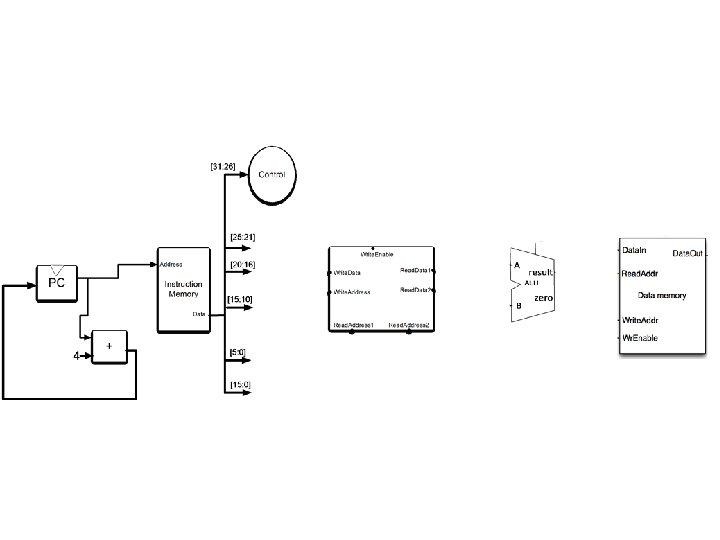
Using memory for data • Load word • Store word 1. Draw the “Data Memory” on the right side of your processor 2. Using the RTL above, add circuitry that is sufficient for executing load word (lw). • Assume that you have a 1 -bit control signal is. LW (1 when instruction is a lw, 0 otherwise) 3. Using the RTL above, add circuitry that is sufficient for executing load word (sw). If you need a control signal, just pick a descriptive name. • Assume that you have a 1 -bit control signal is. SW (1 when instruction is a sw, 0 otherwise)
Branch instructions • beq PC behavior for non branch/jump instructions PC <- PC + 4 1. Add new circuitry or identify existing circuitry used to implement the comparison R[$rs]=R[$rt] 2. Add circuitry to implement Sign. Ext 18 b({imm, 00}). 3. Notice the difference in what happens to the PC register. • Add circuitry to choose between what the next PC is. • Add a new control signal Branch=1 when instruction is a branch instruction, 0 otherwise. • Did you add a MUX? Add necessary logic to calculate its Select input. RTL from http: //www-inst. eecs. berkeley. edu/~cs 61 c/resources/MIPS_help. html
How to control the ALU’s operation opcode funct ALUControl Unit switch (aka, ALUControl) Note that the textbook has a slightly different design where the “main decoder” produces a signal, ALUOp, that tells the ALUDecoder some information based on only the Opcode DDCA, 2 nd Ed Switch
When you just “don’t care” A “don’t care” is where you put an X in the truth table to indicate that it doesn’t matter if the bit is a 0 or a 1. X’s can drastically simplify the truth table and the resulting combinational logic circuit. Why? The person/tool simplifying the circuit can pick whether a 1 or 0 for the X makes the circuit simpler. Example from your recent experience. . . “What should happen to the Soda Machine FSM when Dime and Nickel inputs are both 1 in the same clock period? ” • If our circuit’s behavior is unspecified for a certain input case then we can put X’s into the truth table. You can also put X’s in the output column • an X in the output means that you don’t care what the output is for a certain input case • if you use Logisim’s logic analyzer, be aware that it allows for X’s in the output bits but not the input bits Do not confuse “don’t cares” (X’s in the truth table) with Logisim’s RED wires (i. e. , wires where the value has X’s in it). Red wires are always bad.
Logic analyzer in Logisim Let’s automatically generate the gates for a truth table A B Z 0 0 1 x 1 0 0 1 1. Create Pins for A, B, Z (limitation: must be 1 bit) 2. Project | Analyze circuit 3. In Table tab, enter your truth table values can include “don’t cares” in the output 4. Click Build Circuit 5. Can click through default options. You get an implementation!
Control unit truth table Instruction Opcode Regwrite Reg. Dst ALUSrc Branch Mem. Write Mem. To. Reg ALU operation R-type 0 0 addiu lw sw beq 000000 1 0 depends add
Control unit truth table Instruction Opcode Regwrite Reg. Dst ALUSrc Branch Mem. Write Mem. To. Reg ALU operation R-type 0 0 addiu lw sw beq 000000 1 0 depends add