ARM Tachnology 1 Chapter 4 General Purpose and




- Slides: 43

ARM Tachnology 1

Chapter 4 General Purpose and Alternate Function I/O (GPIO and AFIO) 2

CONTENTS Objectives GPIO Features GPIO Configuration Modes Circuit structure of STM 32 GPIO Configuration 3

4. 1 Objectives Using GPIOs, users can control other devices. In this part, STM 32 GPIOs are introduced including features, structures, configuration and application using firmware library. 4

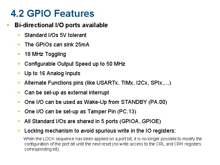
4. 2 GPIO Features Bi-directional I/O ports available Standard I/Os 5 V tolerant The GPIOs can sink 25 m. A 18 MHz Toggling Configurable Output Speed up to 50 MHz Up to 16 Analog Inputs Alternate Functions pins (like USARTx, TIMx, I 2 Cx, SPIx, …) Can be set-up as external interrupt One I/O can be used as Wake-Up from STANDBY (PA. 00) One I/O can be set-up as Tamper Pin (PC. 13) All Standard I/Os are shared in 5 ports (GPIOA. . GPIOE) Locking mechanism to avoid spurious write in the IO registers: When the LOCK sequence has been applied on a port bit, it is no longer possible to modify the configuration of the port bit until the next reset (no write access to the CRL and CRH registers corresponding bit).

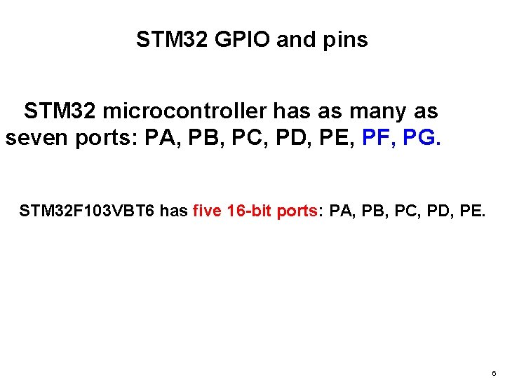
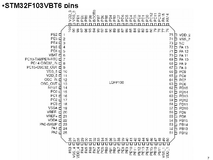
STM 32 GPIO and pins STM 32 microcontroller has as many as seven ports: PA, PB, PC, PD, PE, PF, PG. STM 32 F 103 VBT 6 has five 16 -bit ports: PA, PB, PC, PD, PE. 6

• STM 32 F 103 VBT 6 pins 7

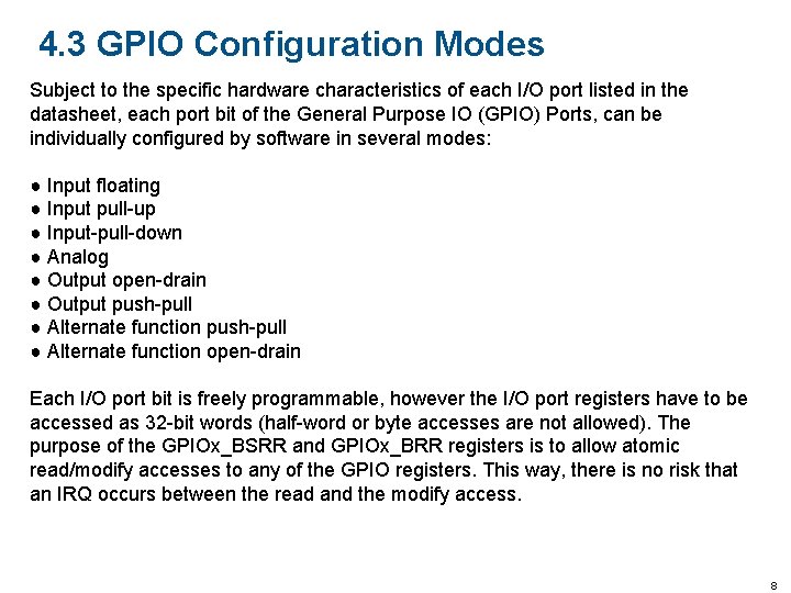
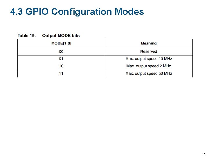
4. 3 GPIO Configuration Modes Subject to the specific hardware characteristics of each I/O port listed in the datasheet, each port bit of the General Purpose IO (GPIO) Ports, can be individually configured by software in several modes: ● Input floating ● Input pull-up ● Input-pull-down ● Analog ● Output open-drain ● Output push-pull ● Alternate function open-drain Each I/O port bit is freely programmable, however the I/O port registers have to be accessed as 32 -bit words (half-word or byte accesses are not allowed). The purpose of the GPIOx_BSRR and GPIOx_BRR registers is to allow atomic read/modify accesses to any of the GPIO registers. This way, there is no risk that an IRQ occurs between the read and the modify access. 8

4. 3 GPIO Configuration Modes

4. 3 GPIO Configuration Modes 10

4. 3 GPIO Configuration Modes 11

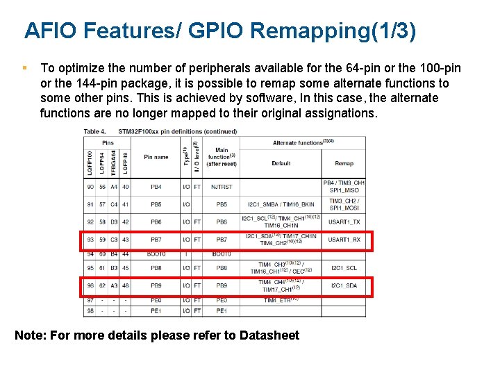
AFIO Features/ GPIO Remapping(1/3) To optimize the number of peripherals available for the 64 -pin or the 100 -pin or the 144 -pin package, it is possible to remap some alternate functions to some other pins. This is achieved by software, In this case, the alternate functions are no longer mapped to their original assignations. Note: For more details please refer to Datasheet

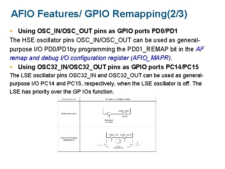
AFIO Features/ GPIO Remapping(2/3) Using OSC_IN/OSC_OUT pins as GPIO ports PD 0/PD 1 The HSE oscillator pins OSC_IN/OSC_OUT can be used as generalpurpose I/O PD 0/PD 1 by programming the PD 01_REMAP bit in the AF remap and debug I/O configuration register (AFIO_MAPR). Using OSC 32_IN/OSC 32_OUT pins as GPIO ports PC 14/PC 15 The LSE oscillator pins OSC 32_IN and OSC 32_OUT can be used as generalpurpose I/O PC 14 and PC 15, respectively, when the LSE oscillator is off. The LSE has priority over the GP IOs function.

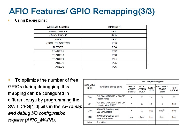
AFIO Features/ GPIO Remapping(3/3) Using Debug pins: To optimize the number of free GPIOs during debugging, this mapping can be configured in different ways by programming the SWJ_CFG[1: 0] bits in the AF remap and debug I/O configuration register (AFIO_MAPR).

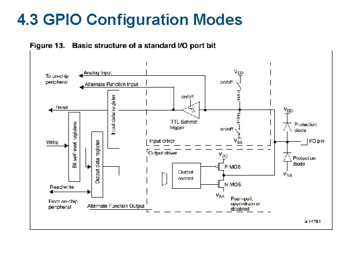
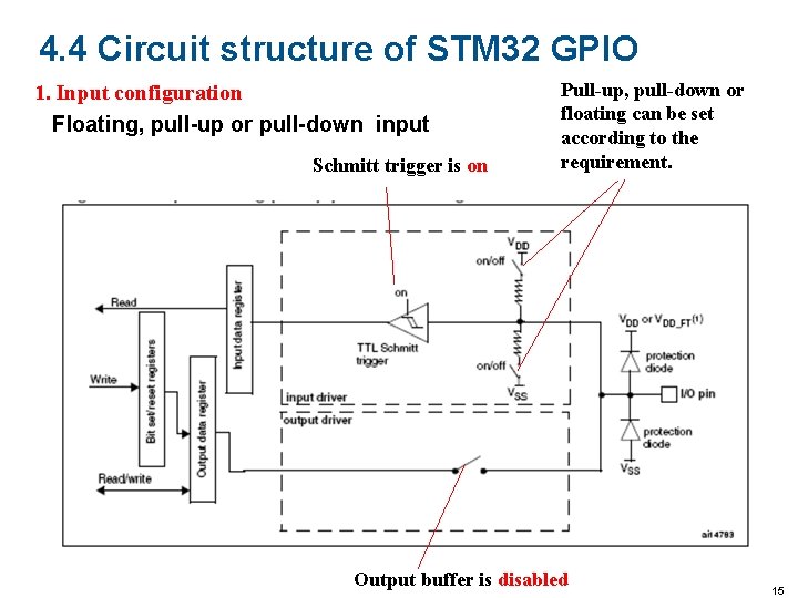
4. 4 Circuit structure of STM 32 GPIO 1. Input configuration Floating, pull-up or pull-down input Schmitt trigger is on Pull-up, pull-down or floating can be set according to the requirement. Output buffer is disabled 15

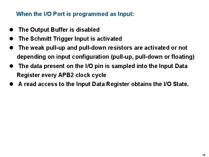
When the I/O Port is programmed as Input: l The Output Buffer is disabled l The Schmitt Trigger Input is activated l The weak pull-up and pull-down resistors are activated or not depending on input configuration (pull-up, pull-down or floating) l The data present on the I/O pin is sampled into the Input Data Register every APB 2 clock cycle l A read access to the Input Data Register obtains the I/O State. 16

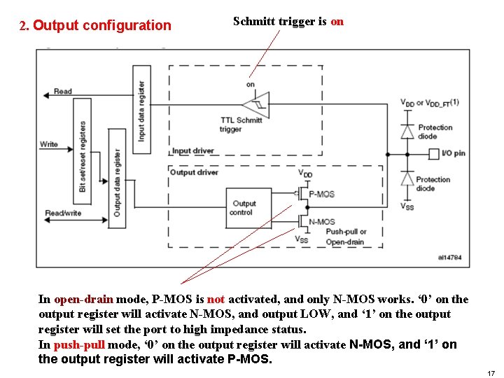
2. Output configuration Schmitt trigger is on In open-drain mode, P-MOS is not activated, and only N-MOS works. ‘ 0’ on the output register will activate N-MOS, and output LOW, and ‘ 1’ on the output register will set the port to high impedance status. In push-pull mode, ‘ 0’ on the output register will activate N-MOS, and ‘ 1’ on the output register will activate P-MOS. 17

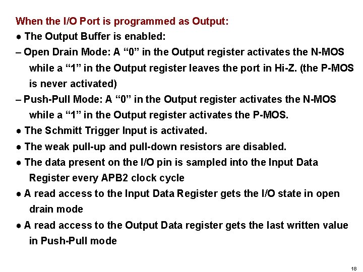
When the I/O Port is programmed as Output: ● The Output Buffer is enabled: – Open Drain Mode: A “ 0” in the Output register activates the N-MOS while a “ 1” in the Output register leaves the port in Hi-Z. (the P-MOS is never activated) – Push-Pull Mode: A “ 0” in the Output register activates the N-MOS while a “ 1” in the Output register activates the P-MOS. ● The Schmitt Trigger Input is activated. ● The weak pull-up and pull-down resistors are disabled. ● The data present on the I/O pin is sampled into the Input Data Register every APB 2 clock cycle ● A read access to the Input Data Register gets the I/O state in open drain mode ● A read access to the Output Data register gets the last written value in Push-Pull mode 18

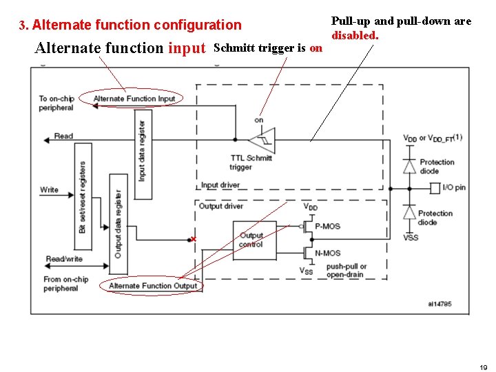
3. Alternate function configuration Alternate function input Schmitt trigger is on Pull-up and pull-down are disabled. × 19

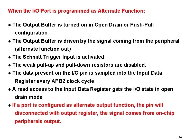
When the I/O Port is programmed as Alternate Function: ● The Output Buffer is turned on in Open Drain or Push-Pull configuration ● The Output Buffer is driven by the signal coming from the peripheral (alternate function out) ● The Schmitt Trigger Input is activated ● The weak pull-up and pull-down resistors are disabled. ● The data present on the I/O pin is sampled into the Input Data Register every APB 2 clock cycle ● A read access to the Input Data Register gets the I/O state in open drain mode ● If a port is configured as alternate output function, the pin will disconnected with output register, the signal comes from on-chip peripherals output. 20

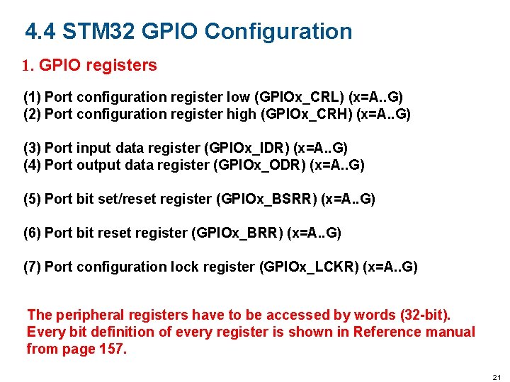
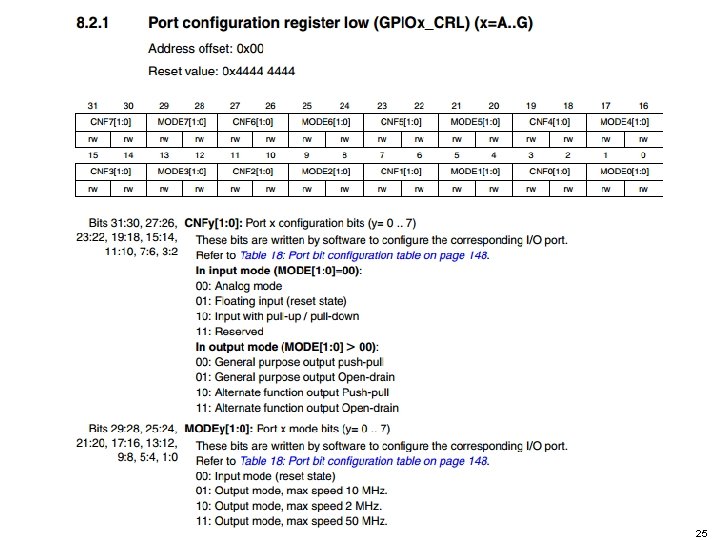
4. 4 STM 32 GPIO Configuration 1. GPIO registers (1) Port configuration register low (GPIOx_CRL) (x=A. . G) (2) Port configuration register high (GPIOx_CRH) (x=A. . G) (3) Port input data register (GPIOx_IDR) (x=A. . G) (4) Port output data register (GPIOx_ODR) (x=A. . G) (5) Port bit set/reset register (GPIOx_BSRR) (x=A. . G) (6) Port bit reset register (GPIOx_BRR) (x=A. . G) (7) Port configuration lock register (GPIOx_LCKR) (x=A. . G) The peripheral registers have to be accessed by words (32 -bit). Every bit definition of every register is shown in Reference manual from page 157. 21

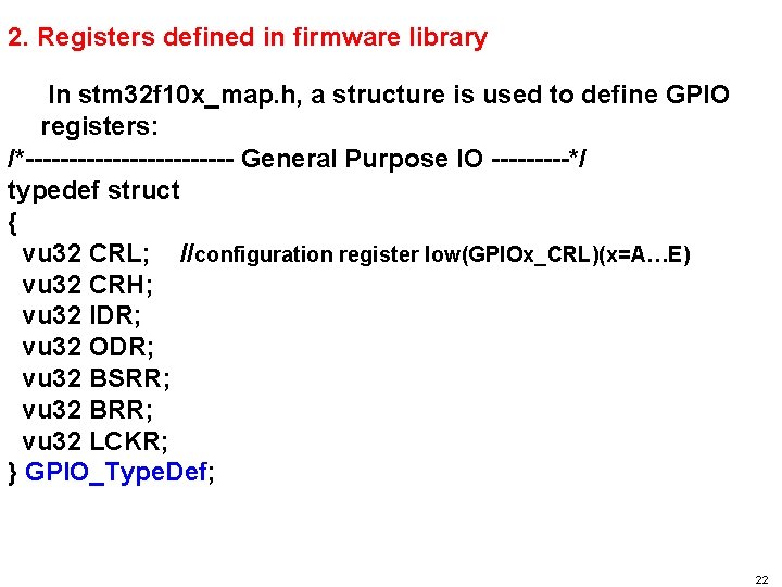
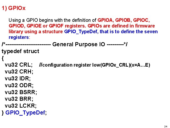
2. Registers defined in firmware library In stm 32 f 10 x_map. h, a structure is used to define GPIO registers: /*------------ General Purpose IO -----*/ typedef struct { vu 32 CRL; //configuration register low(GPIOx_CRL)(x=A…E) vu 32 CRH; vu 32 IDR; vu 32 ODR; vu 32 BSRR; vu 32 BRR; vu 32 LCKR; } GPIO_Type. Def; 22

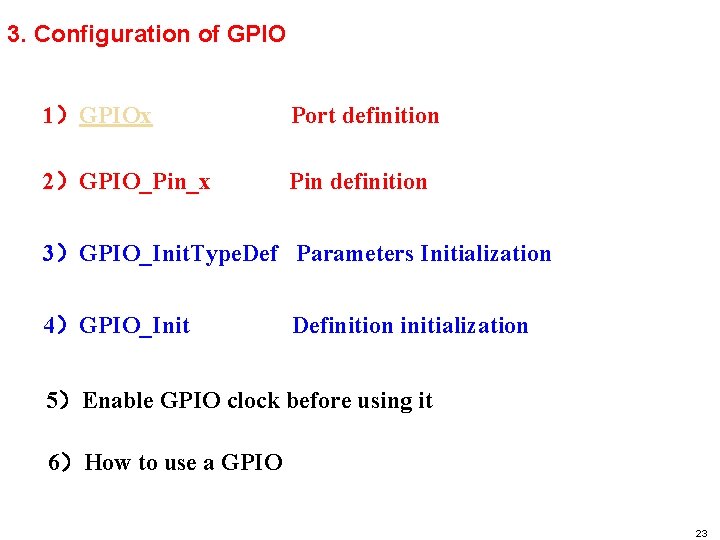
3. Configuration of GPIO 1)GPIOx Port definition 2)GPIO_Pin_x Pin definition 3)GPIO_Init. Type. Def Parameters Initialization 4)GPIO_Init Definition initialization 5)Enable GPIO clock before using it 6)How to use a GPIO 23

1) GPIOx Using a GPIO begins with the definition of GPIOA, GPIOB, GPIOC, GPIOD, GPIOE or GPIOF registers. GPIOs are defined in firmware library using a structure GPIO_Type. Def, that is to define the seven registers: /*------------ General Purpose IO -----*/ typedef struct { vu 32 CRL; //configuration register low(GPIOx_CRL)(x=A…E) vu 32 CRH; vu 32 IDR; vu 32 ODR; vu 32 BSRR; vu 32 BRR; vu 32 LCKR; } GPIO_Type. Def; 24

25

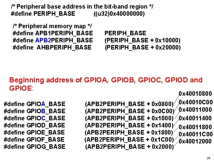
/* Peripheral base address in the bit-band region */ #define PERIPH_BASE ((u 32)0 x 40000000) /* Peripheral memory map */ #define APB 1 PERIPH_BASE #define APB 2 PERIPH_BASE #define AHBPERIPH_BASE (PERIPH_BASE + 0 x 10000) (PERIPH_BASE + 0 x 20000) Beginning address of GPIOA, GPIOB, GPIOC, GPIOD and GPIOE: #define GPIOA_BASE #define GPIOB_BASE #define GPIOC_BASE #define GPIOD_BASE #define GPIOE_BASE #define GPIOF_BASE #define GPIOG_BASE (APB 2 PERIPH_BASE + 0 x 0800) (APB 2 PERIPH_BASE + 0 x 0 C 00) (APB 2 PERIPH_BASE + 0 x 1000) (APB 2 PERIPH_BASE + 0 x 1400) (APB 2 PERIPH_BASE + 0 x 1800) (APB 2 PERIPH_BASE + 0 x 1 C 00) (APB 2 PERIPH_BASE + 0 x 2000) 0 x 40010800 0 x 40010 C 00 0 x 40011000 0 x 40011400 0 x 40011800 0 x 40011 C 00 0 x 40012000 26

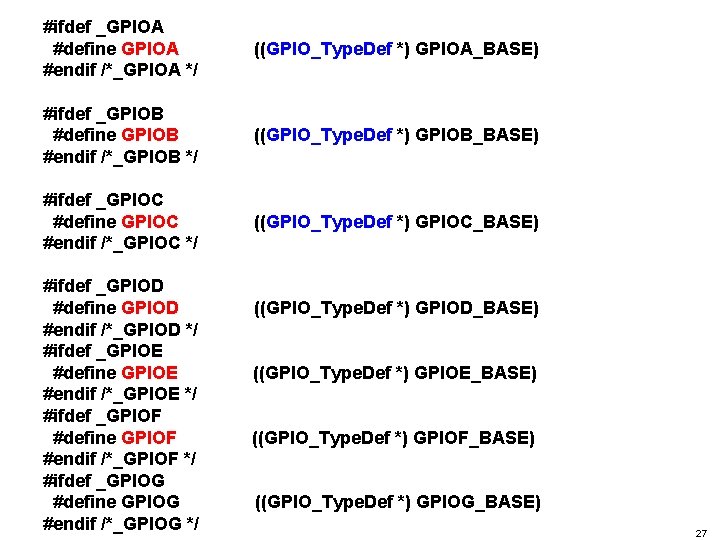
#ifdef _GPIOA #define GPIOA #endif /*_GPIOA */ ((GPIO_Type. Def *) GPIOA_BASE) #ifdef _GPIOB #define GPIOB #endif /*_GPIOB */ ((GPIO_Type. Def *) GPIOB_BASE) #ifdef _GPIOC #define GPIOC #endif /*_GPIOC */ ((GPIO_Type. Def *) GPIOC_BASE) #ifdef _GPIOD #define GPIOD #endif /*_GPIOD */ #ifdef _GPIOE #define GPIOE #endif /*_GPIOE */ #ifdef _GPIOF #define GPIOF #endif /*_GPIOF */ #ifdef _GPIOG #define GPIOG #endif /*_GPIOG */ ((GPIO_Type. Def *) GPIOD_BASE) ((GPIO_Type. Def *) GPIOE_BASE) ((GPIO_Type. Def *) GPIOF_BASE) ((GPIO_Type. Def *) GPIOG_BASE) 27

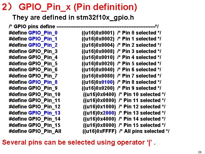
2) GPIO_Pin_x (Pin definition) They are defined in stm 32 f 10 x_gpio. h /* GPIO pins define -----------------------------*/ #define GPIO_Pin_0 ((u 16)0 x 0001) /* Pin 0 selected */ #define GPIO_Pin_1 ((u 16)0 x 0002) /* Pin 1 selected */ #define GPIO_Pin_2 ((u 16)0 x 0004) /* Pin 2 selected */ #define GPIO_Pin_3 ((u 16)0 x 0008) /* Pin 3 selected */ #define GPIO_Pin_4 ((u 16)0 x 0010) /* Pin 4 selected */ #define GPIO_Pin_5 ((u 16)0 x 0020) /* Pin 5 selected */ #define GPIO_Pin_6 ((u 16)0 x 0040) /* Pin 6 selected */ #define GPIO_Pin_7 ((u 16)0 x 0080) /* Pin 7 selected */ #define GPIO_Pin_8 ((u 16)0 x 0100) /* Pin 8 selected */ #define GPIO_Pin_9 ((u 16)0 x 0200) /* Pin 9 selected */ #define GPIO_Pin_10 ((u 16)0 x 0400) /* Pin 10 selected */ #define GPIO_Pin_11 ((u 16)0 x 0800) /* Pin 11 selected */ #define GPIO_Pin_12 ((u 16)0 x 1000) /* Pin 12 selected */ #define GPIO_Pin_13 ((u 16)0 x 2000) /* Pin 13 selected */ #define GPIO_Pin_14 ((u 16)0 x 4000) /* Pin 14 selected */ #define GPIO_Pin_15 ((u 16)0 x 8000) /* Pin 15 selected */ #define GPIO_Pin_All ((u 16)0 x. FFFF) /* All pins selected */ Several pins can be selected using operator ‘|’. 28

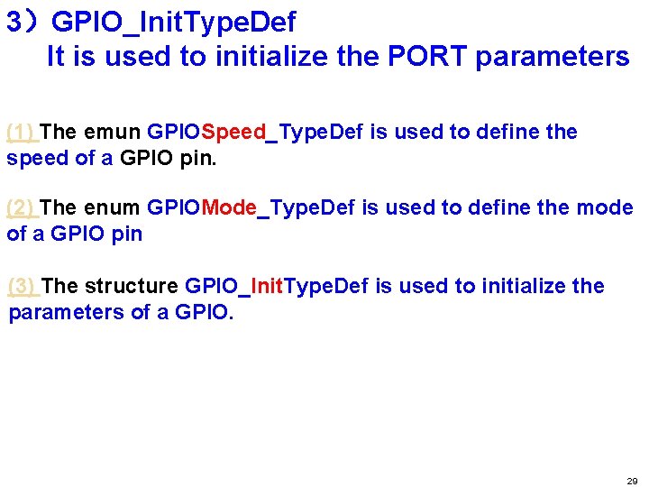
3)GPIO_Init. Type. Def It is used to initialize the PORT parameters (1) The emun GPIOSpeed_Type. Def is used to define the speed of a GPIO pin. (2) The enum GPIOMode_Type. Def is used to define the mode of a GPIO pin (3) The structure GPIO_Init. Type. Def is used to initialize the parameters of a GPIO. 29

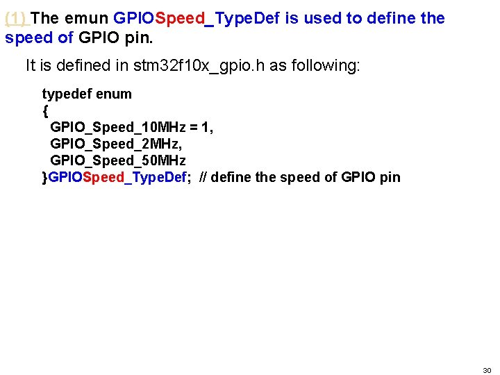
(1) The emun GPIOSpeed_Type. Def is used to define the speed of GPIO pin. It is defined in stm 32 f 10 x_gpio. h as following: typedef enum { GPIO_Speed_10 MHz = 1, GPIO_Speed_2 MHz, GPIO_Speed_50 MHz }GPIOSpeed_Type. Def; // define the speed of GPIO pin 30

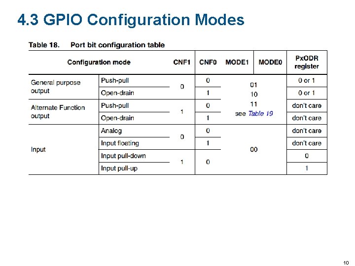
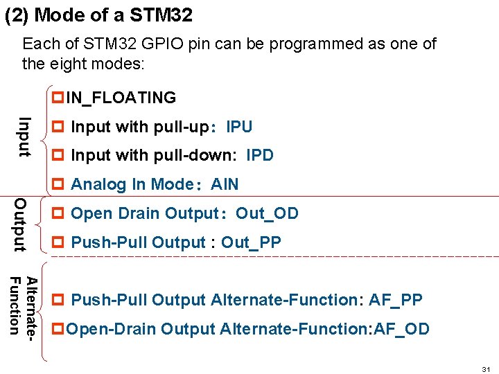
(2) Mode of a STM 32 Each of STM 32 GPIO pin can be programmed as one of the eight modes: p. IN_FLOATING Input p Input with pull-up: IPU p Input with pull-down: IPD p Analog In Mode: AIN Output p Open Drain Output: Out_OD p Push-Pull Output : Out_PP Alternate. Function p Push-Pull Output Alternate-Function: AF_PP p. Open-Drain Output Alternate-Function: AF_OD 31

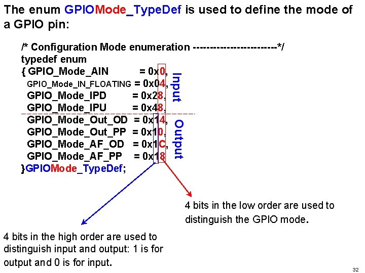
The enum GPIOMode_Type. Def is used to define the mode of a GPIO pin: Input /* Configuration Mode enumeration -------------*/ typedef enum { GPIO_Mode_AIN = 0 x 0, GPIO_Mode_IN_FLOATING = 0 x 04, GPIO_Mode_IPD = 0 x 28, GPIO_Mode_IPU = 0 x 48, GPIO_Mode_Out_OD = 0 x 14, GPIO_Mode_Out_PP = 0 x 10, GPIO_Mode_AF_OD = 0 x 1 C, GPIO_Mode_AF_PP = 0 x 18 }GPIOMode_Type. Def; Output 4 bits in the low order are used to distinguish the GPIO mode. 4 bits in the high order are used to distinguish input and output: 1 is for output and 0 is for input. 32

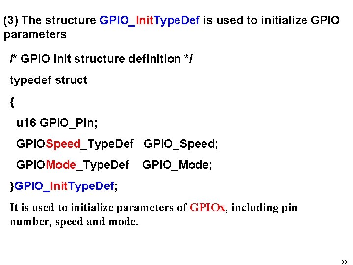
(3) The structure GPIO_Init. Type. Def is used to initialize GPIO parameters /* GPIO Init structure definition */ typedef struct { u 16 GPIO_Pin; GPIOSpeed_Type. Def GPIO_Speed; GPIOMode_Type. Def GPIO_Mode; }GPIO_Init. Type. Def; It is used to initialize parameters of GPIOx, including pin number, speed and mode. 33

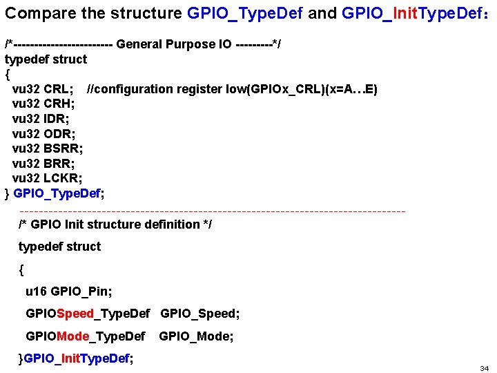
Compare the structure GPIO_Type. Def and GPIO_Init. Type. Def: /*------------ General Purpose IO -----*/ typedef struct { vu 32 CRL; //configuration register low(GPIOx_CRL)(x=A…E) vu 32 CRH; vu 32 IDR; vu 32 ODR; vu 32 BSRR; vu 32 BRR; vu 32 LCKR; } GPIO_Type. Def; /* GPIO Init structure definition */ typedef struct { u 16 GPIO_Pin; GPIOSpeed_Type. Def GPIO_Speed; GPIOMode_Type. Def }GPIO_Init. Type. Def; GPIO_Mode; 34

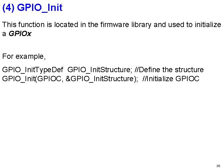
(4) GPIO_Init This function is located in the firmware library and used to initialize a GPIOx For example, GPIO_Init. Type. Def GPIO_Init. Structure; //Define the structure GPIO_Init(GPIOC, &GPIO_Init. Structure); //Initialize GPIOC 35

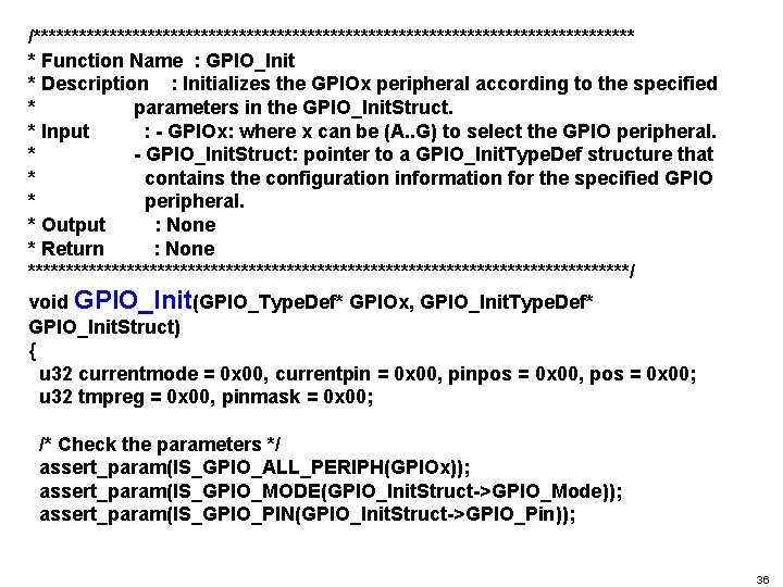
/**************************************** * Function Name : GPIO_Init * Description : Initializes the GPIOx peripheral according to the specified * parameters in the GPIO_Init. Struct. * Input : - GPIOx: where x can be (A. . G) to select the GPIO peripheral. * - GPIO_Init. Struct: pointer to a GPIO_Init. Type. Def structure that * contains the configuration information for the specified GPIO * peripheral. * Output : None * Return : None ****************************************/ void GPIO_Init(GPIO_Type. Def* GPIOx, GPIO_Init. Type. Def* GPIO_Init. Struct) { u 32 currentmode = 0 x 00, currentpin = 0 x 00, pinpos = 0 x 00, pos = 0 x 00; u 32 tmpreg = 0 x 00, pinmask = 0 x 00; /* Check the parameters */ assert_param(IS_GPIO_ALL_PERIPH(GPIOx)); assert_param(IS_GPIO_MODE(GPIO_Init. Struct->GPIO_Mode)); assert_param(IS_GPIO_PIN(GPIO_Init. Struct->GPIO_Pin)); 36

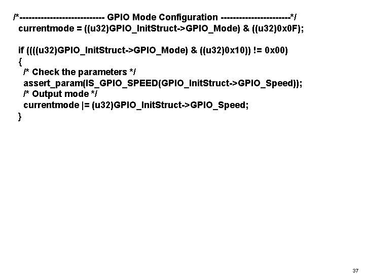
/*-------------- GPIO Mode Configuration ------------*/ currentmode = ((u 32)GPIO_Init. Struct->GPIO_Mode) & ((u 32)0 x 0 F); if ((((u 32)GPIO_Init. Struct->GPIO_Mode) & ((u 32)0 x 10)) != 0 x 00) { /* Check the parameters */ assert_param(IS_GPIO_SPEED(GPIO_Init. Struct->GPIO_Speed)); /* Output mode */ currentmode |= (u 32)GPIO_Init. Struct->GPIO_Speed; } 37

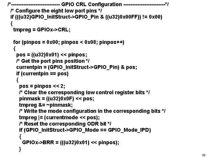
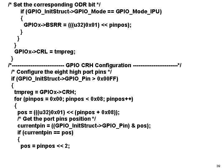
/*-------------- GPIO CRL Configuration ------------*/ /* Configure the eight low port pins */ if (((u 32)GPIO_Init. Struct->GPIO_Pin & ((u 32)0 x 00 FF)) != 0 x 00) { tmpreg = GPIOx->CRL; for (pinpos = 0 x 00; pinpos < 0 x 08; pinpos++) { pos = ((u 32)0 x 01) << pinpos; /* Get the port pins position */ currentpin = (GPIO_Init. Struct->GPIO_Pin) & pos; if (currentpin == pos) { pos = pinpos << 2; /* Clear the corresponding low control register bits */ pinmask = ((u 32)0 x 0 F) << pos; tmpreg &= ~pinmask; /* Write the mode configuration in the corresponding bits */ tmpreg |= (currentmode << pos); /* Reset the corresponding ODR bit */ if (GPIO_Init. Struct->GPIO_Mode == GPIO_Mode_IPD) { GPIOx->BRR = (((u 32)0 x 01) << pinpos); } 38

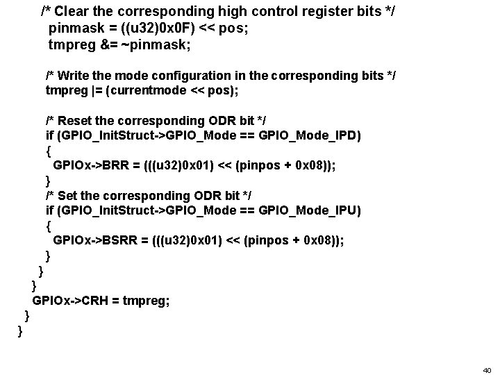
/* Set the corresponding ODR bit */ if (GPIO_Init. Struct->GPIO_Mode == GPIO_Mode_IPU) { GPIOx->BSRR = (((u 32)0 x 01) << pinpos); } } } GPIOx->CRL = tmpreg; } /*-------------- GPIO CRH Configuration ------------*/ /* Configure the eight high port pins */ if (GPIO_Init. Struct->GPIO_Pin > 0 x 00 FF) { tmpreg = GPIOx->CRH; for (pinpos = 0 x 00; pinpos < 0 x 08; pinpos++) { pos = (((u 32)0 x 01) << (pinpos + 0 x 08)); /* Get the port pins position */ currentpin = ((GPIO_Init. Struct->GPIO_Pin) & pos); if (currentpin == pos) { pos = pinpos << 2; 39

/* Clear the corresponding high control register bits */ pinmask = ((u 32)0 x 0 F) << pos; tmpreg &= ~pinmask; /* Write the mode configuration in the corresponding bits */ tmpreg |= (currentmode << pos); /* Reset the corresponding ODR bit */ if (GPIO_Init. Struct->GPIO_Mode == GPIO_Mode_IPD) { GPIOx->BRR = (((u 32)0 x 01) << (pinpos + 0 x 08)); } /* Set the corresponding ODR bit */ if (GPIO_Init. Struct->GPIO_Mode == GPIO_Mode_IPU) { GPIOx->BSRR = (((u 32)0 x 01) << (pinpos + 0 x 08)); } } } GPIOx->CRH = tmpreg; } } 40

6)How to use a GPIO Please see the video 41

Now you are able to… Develop your application on STM 32 F 103 device using GPIO

Thank you 43