
Architecture of Datapathoriented Coarsegrain Logic and Routing for
- Slides: 30
Architecture of Datapathoriented Coarse-grain Logic and Routing for FPGAs Andy Ye, Jonathan Rose, David Lewis Department of Electrical and Computer Engineering University of Toronto {yeandy, jayar, lewis}@eecg. utoronto. ca 1
Outline • Motivation – Datapath regularity • An datapath-oriented FPGA – Architecture – CAD flow • Experimental results – Area efficiency • Conclusion 2
Modern FPGAs • Very large logic capacities – Over 10 million equivalent logic gates • Increasingly used to implement large and complex applications – Central processing units – Graphics accelerators – Digital signal processors – Packet switching networks 3
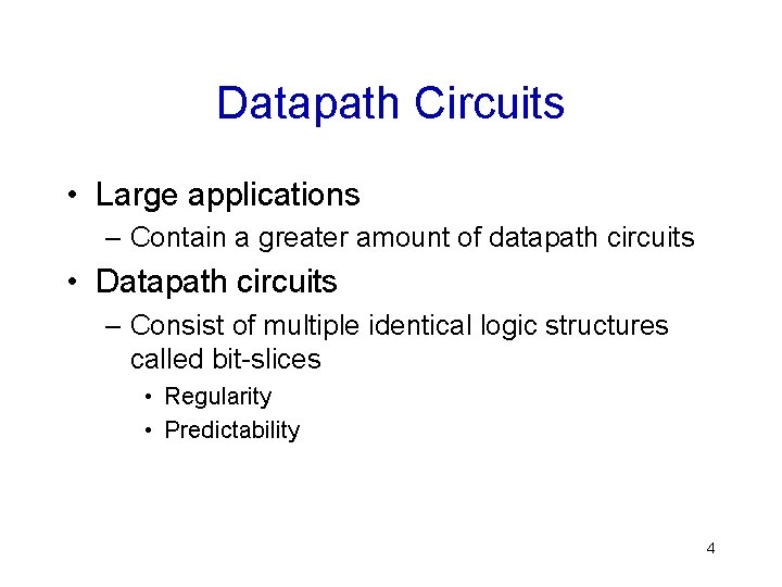
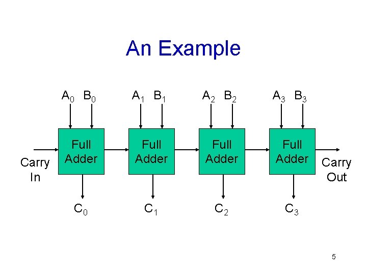
Datapath Circuits • Large applications – Contain a greater amount of datapath circuits • Datapath circuits – Consist of multiple identical logic structures called bit-slices • Regularity • Predictability 4
An Example Carry In A 0 B 0 A 1 B 1 A 2 B 2 A 3 B 3 Full Adder C 0 C 1 C 2 C 3 Carry Out 5
An Example 6
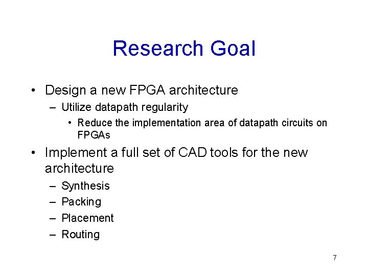
Research Goal • Design a new FPGA architecture – Utilize datapath regularity • Reduce the implementation area of datapath circuits on FPGAs • Implement a full set of CAD tools for the new architecture – – Synthesis Packing Placement Routing 7
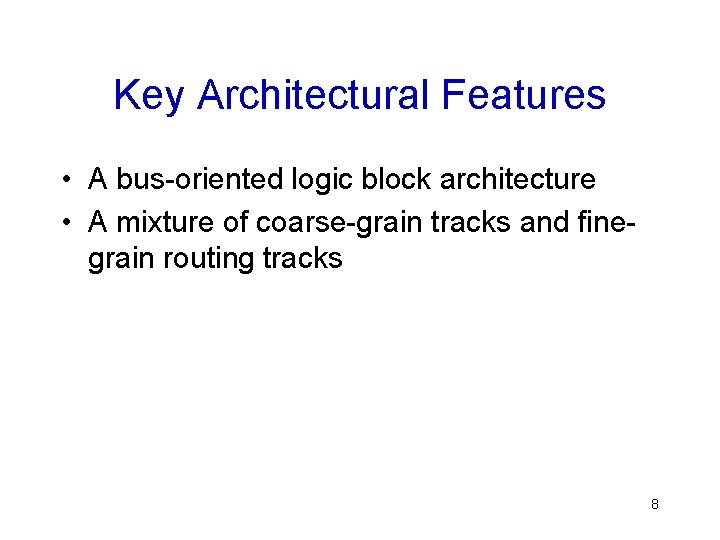
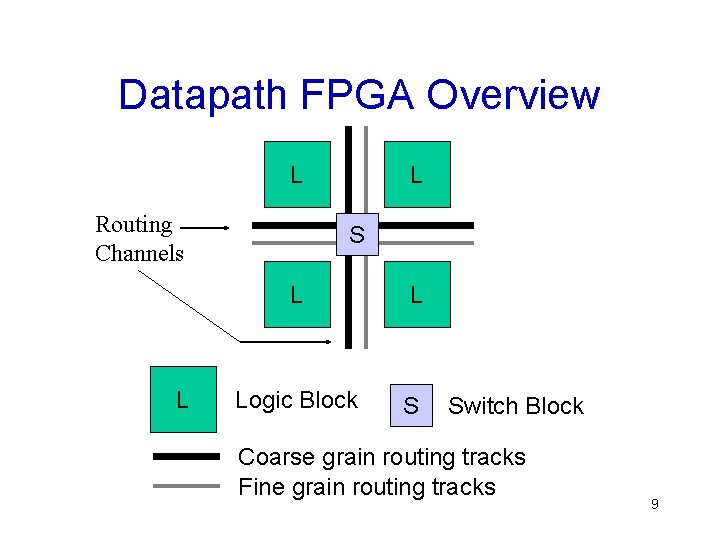
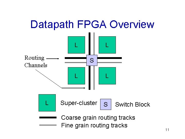
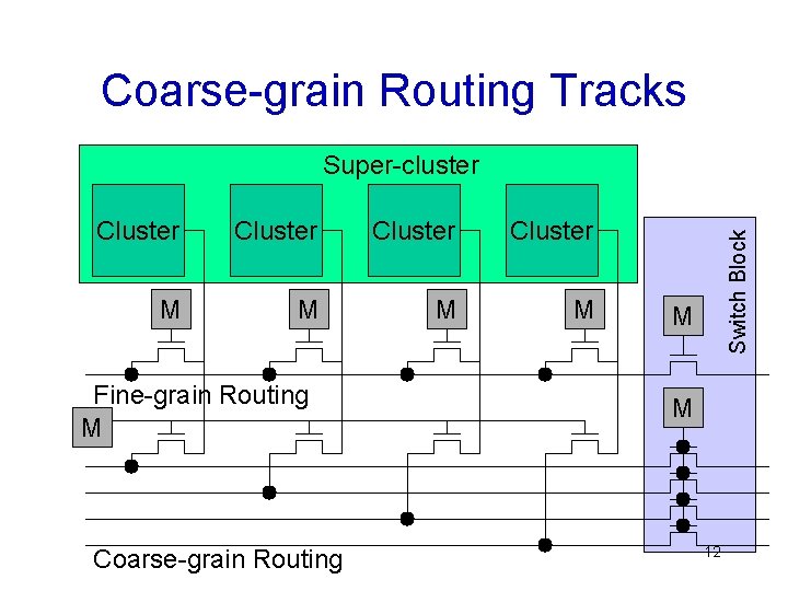
Key Architectural Features • A bus-oriented logic block architecture • A mixture of coarse-grain tracks and finegrain routing tracks 8
Datapath FPGA Overview L Routing Channels L L S L L Logic Block S Switch Block Coarse grain routing tracks Fine grain routing tracks 9
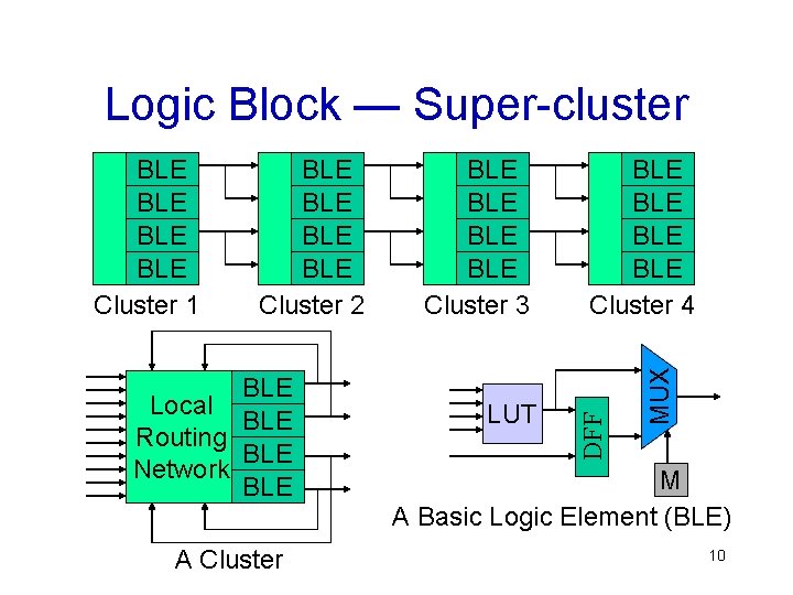
Logic Block — Super-cluster BLE Local BLE Routing BLE Network BLE A Cluster BLE BLE Cluster 3 LUT BLE BLE Cluster 4 MUX BLE BLE Cluster 2 DFF BLE BLE Cluster 1 M A Basic Logic Element (BLE) 10
Datapath FPGA Overview L Routing Channels L S L L Super-cluster L S Switch Block Coarse grain routing tracks Fine grain routing tracks 11
Coarse-grain Routing Tracks Cluster M M Fine-grain Routing M Coarse-grain Routing Switch Block Super-cluster M M 12
CAD Flow • CAD flow for the datapath-oriented FPGA consists of – Synthesis – Packing – Placement – Routing • Conventional CAD flow – Minimize area and delay metrics – Destroy datapath regularity 13
Datapath-oriented CAD Flow • Preserve datapath regularity (bit-sliced structures) • Map the preserved regularity onto the datapath-oriented FPGA architecture • Maximize the utilization of coarse-grain routing tracks – Minimize the implementation area of datapath structures 14
Datapath Representation • Datapath circuits are represent by netlists of datapath components (VHDL or Verilog) • Datapath component library – – – Multiplexers Adders/subtracters Shifters Comparators Registers • Each component consists of identical bit-slices 15
Synthesis • Enhanced module compaction algorithm • Based on the Synopsys FPGA compiler • Augmented with several datapath-oriented features – Preserve datapath regularity by preserving bitslice boundaries – Achieve as good area results as the conventional synthesis tools 16
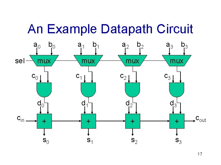
An Example Datapath Circuit a 0 sel b 0 mux c 0 b 1 mux c 1 d 0 cin a 1 a 2 b 2 mux c 2 d 1 a 3 b 3 mux c 3 d 2 d 3 + + s 0 s 1 s 2 s 3 cout 17
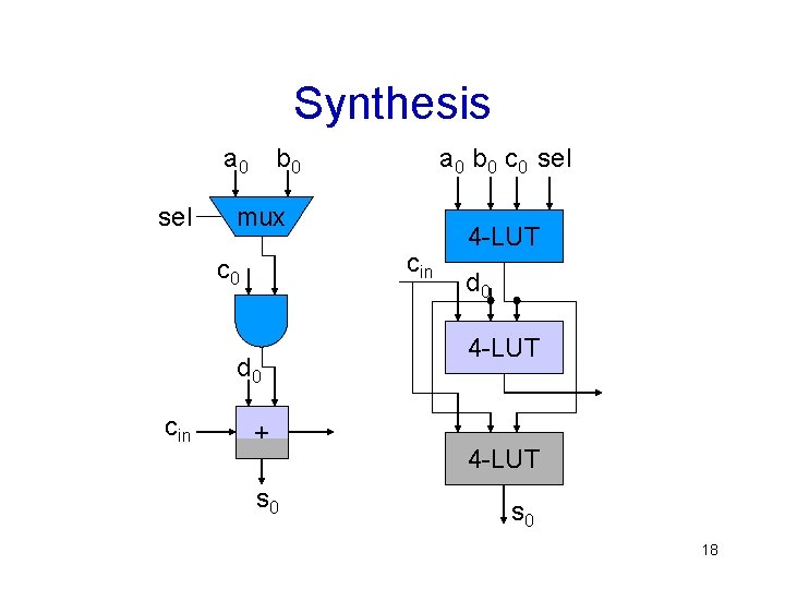
Synthesis a 0 sel b 0 mux cin c 0 d 0 cin a 0 b 0 c 0 sel + s 0 4 -LUT d 0 4 -LUT s 0 18
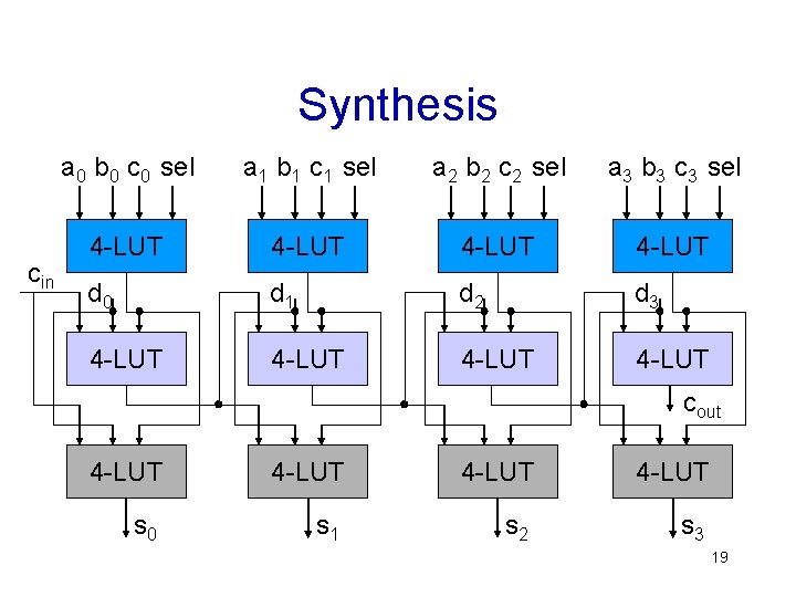
Synthesis cin a 0 b 0 c 0 sel a 1 b 1 c 1 sel a 2 b 2 c 2 sel a 3 b 3 c 3 sel 4 -LUT d 0 d 1 d 2 d 3 4 -LUT cout 4 -LUT s 0 s 1 s 2 s 3 19
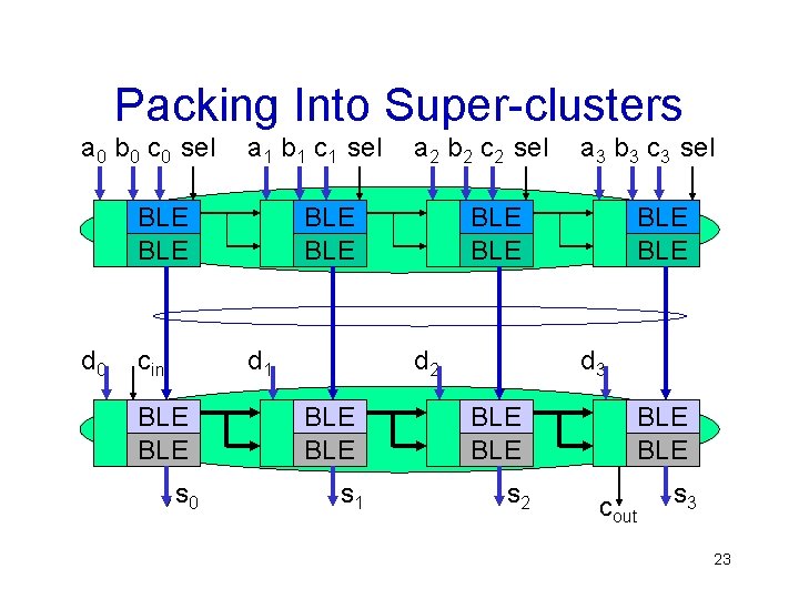
Packing • Based on the T-VPACK packing algorithm • Pack adjacent bit-slices into super-clusters • Utilize carry connections in super-clusters to minimize the delay of carry chains 20
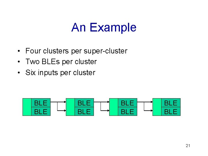
An Example • Four clusters per super-cluster • Two BLEs per cluster • Six inputs per cluster BLE BLE 21
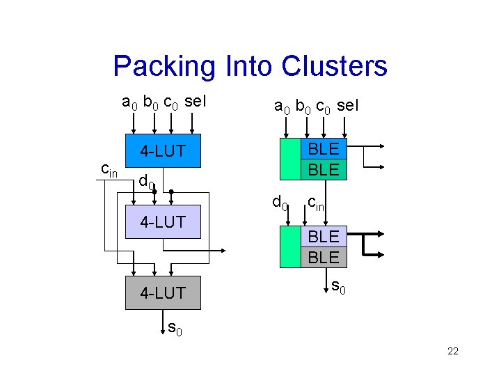
Packing Into Clusters a 0 b 0 c 0 sel cin a 0 b 0 c 0 sel BLE 4 -LUT d 0 cin BLE s 0 22
Packing Into Super-clusters a 0 b 0 c 0 sel a 1 b 1 c 1 sel BLE d 0 cin BLE d 1 BLE s 0 a 2 b 2 c 2 sel BLE d 2 BLE s 1 a 3 b 3 c 3 sel BLE d 3 BLE s 2 BLE cout s 3 23
Placement • Based on the VPR placer • Use simulated annealing algorithm • For super-clusters containing datapath circuits – Move super-clusters only • For super-clusters containing non-datapath circuits - Move individual clusters 24
Routing • Based on the VPR router • Use the path finder algorithm • As much as possible – Route buses through coarse-grain routing tracks – Route individual signals through fine-grain routing tracks • When necessary – Use coarse-grain routing tracks for individual signals – Use fine-grain routing tracks for buses 25
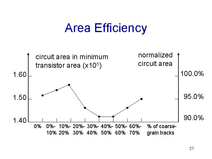
Area Efficiency • Benchmarks – 15 datapath circuits from the Pico-java processor • Architectural assumptions – – – Four BLEs per cluster Four clusters per super-cluster Four coarse-grain tracks sharing configuration memory Logic track length of two Disjoint switch block topology • Architectural variables – Number of coarse-grain tracks 26
Area Efficiency circuit area in minimum transistor area (x 106) normalized circuit area 1. 60 100. 0% 1. 50 95. 0% 1. 40 90. 0% 0% 0%- 10%- 20%- 30%- 40%- 50%- 60%- % of coarse 10% 20% 30% 40% 50% 60% 70% grain tracks 27
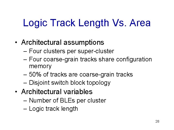
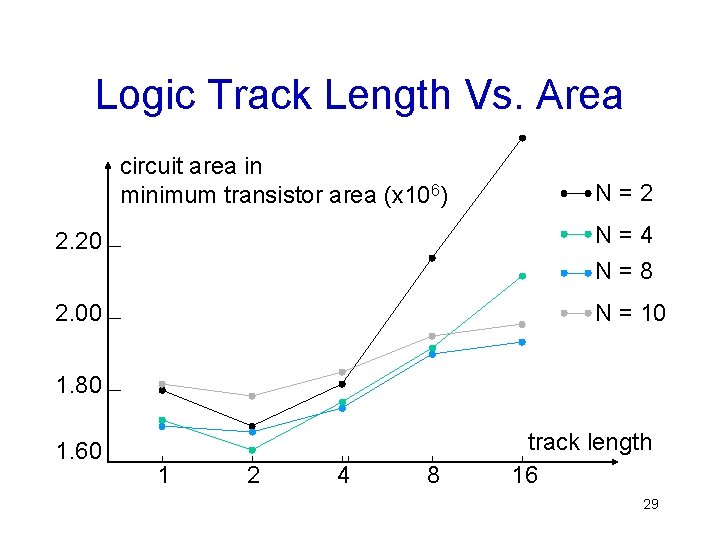
Logic Track Length Vs. Area • Architectural assumptions – Four clusters per super-cluster – Four coarse-grain tracks share configuration memory – 50% of tracks are coarse-grain tracks – Disjoint switch block topology • Architectural variables – Number of BLEs per cluster – Logic track length 28
Logic Track Length Vs. Area circuit area in minimum transistor area (x 106) N=2 2. 20 N=4 N=8 2. 00 N = 10 1. 80 1. 60 1 2 4 8 track length 16 29
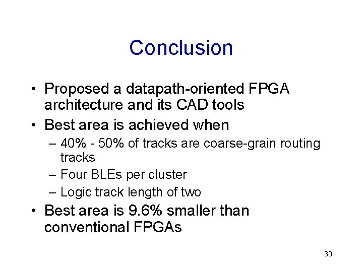
Conclusion • Proposed a datapath-oriented FPGA architecture and its CAD tools • Best area is achieved when – 40% - 50% of tracks are coarse-grain routing tracks – Four BLEs per cluster – Logic track length of two • Best area is 9. 6% smaller than conventional FPGAs 30