APSEL Deep nwell and Deep pwell CMOS Sensors



- Slides: 31

APSEL Deep n-well and Deep p-well CMOS Sensors with ST and Tower. Jazz Technologies Gianluca Traversia, b OUTLINE üIntroduction üDeep n-well CMOS MAPS with ST technology a. Università degli Studi di Bergamo b. INFN üAPSEL Sensor üSDR 0 Sensor üDeep n-well CMOS MAPS with IBM technology üDeep p-well CMOS MAPS with TJ technology Workshop on CMOS Active Pixel Sensors for Particle Tracking (CPIX 14) 15 th – 17 th September 2014, Bonn, Germany

Motivations Ø Experiments at the future high luminosity colliders and B-factories (ILC, Super. B) need fast, highly granular, low material budget particle trackers Ø CMOS monolithic active pixel sensors (MAPS) may provide improved position and momentum resolution Ø based on collection of diffusing charge may be thinned to a few tens of μm, low multiple scattering Ø minimal readout electronics small pitch, high spatial resolution but no PMOS transistors Ø Modern VLSI CMOS processes (180 nm and below) could be exploited to increase the functionality in the elementary cell -> design of MAPS with similar readout functionalities as in hybrid pixels (sparsification, time stamping) Ø A readout architecture with data sparsification could give some advantages with respect to standard, CIS-like MAPS implementations Ø MAPS approach takes advantage of CMOS triple well structures to improve the readout speed of MAPS sensors through pixel level sparsification -> APSEL family and SDR 0 chip Ø A step toward full compliance with the experiment specs may be represented by vertical integration techniques 3 D DNW MAPS integrated in the first run of the 3 D-IC collaboration Ø Depending on the experiment characteristics, MAPS may be required to withstand a total ionizing dose from a few 10 krad to a few Mrad per year (e. g. : Super. B SVT Layer 0 specs: 3 Mrad/yr and 5∙ 1012 1 Me. V neutron equivalent/cm 2/yr, challenging for CMOS MAPS) Ø CMOS MAPS with sparsified readout in a high-resistivity epitaxial layer, deep p-well technology (INMAPS process provided by Tower. Jazz) -> APSEL 4 WELL chip Talk V. Re this morning Talk L. Ratti on Wednesday Workshop on CMOS Active Pixel Sensors for Particle Tracking (CPIX 14), 15 th – 17 th September 2014, Bonn, Germany

Deep n-well MAPS with the 130 nm CMOS STMicroelectronics technology Workshop on CMOS Active Pixel Sensors for Particle Tracking (CPIX 14), 15 th – 17 th September 2014, Bonn, Germany

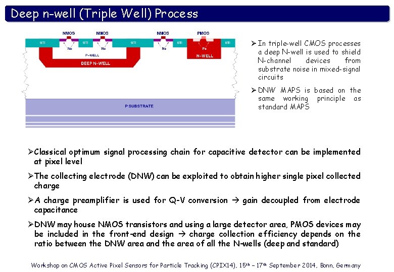
Deep n-well (Triple Well) Process Ø In triple-well CMOS processes a deep N-well is used to shield N-channel devices from substrate noise in mixed-signal circuits Ø DNW MAPS is based on the same working principle as standard MAPS Ø Classical optimum signal processing chain for capacitive detector can be implemented at pixel level Ø The collecting electrode (DNW) can be exploited to obtain higher single pixel collected charge Ø A charge preamplifier is used for Q-V conversion gain decoupled from electrode capacitance Ø DNW may house NMOS transistors and using a large detector area, PMOS devices may be included in the front-end design charge collection efficiency depends on the ratio between the DNW area and the area of all the N-wells (deep and standard) Workshop on CMOS Active Pixel Sensors for Particle Tracking (CPIX 14), 15 th – 17 th September 2014, Bonn, Germany

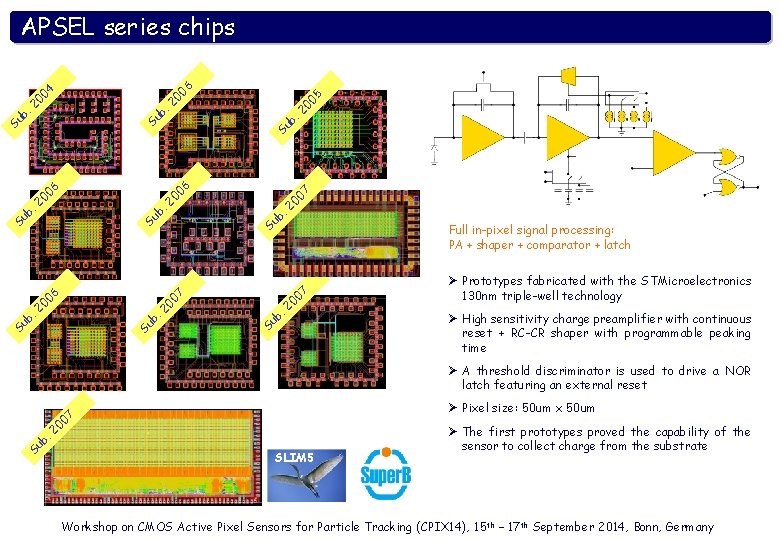
20 05 7 Su b. 20 0 Su b. 7 Full in-pixel signal processing: PA + shaper + comparator + latch 00 b. 2 Su Su Su b. 20 20 07 06 Su b. 20 20 0 6 06 Su b . 2 20 04 00 6 APSEL series chips Ø Prototypes fabricated with the STMicroelectronics 130 nm triple-well technology Ø High sensitivity charge preamplifier with continuous reset + RC-CR shaper with programmable peaking time Ø A threshold discriminator is used to drive a NOR latch featuring an external reset Su b. 2 00 7 Ø Pixel size: 50 um x 50 um SLIM 5 Ø The first prototypes proved the capability of the sensor to collect charge from the substrate Workshop on CMOS Active Pixel Sensors for Particle Tracking (CPIX 14), 15 th – 17 th September 2014, Bonn, Germany

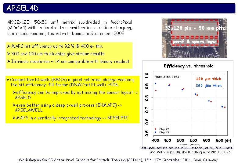
APSEL 4 D 4 K(32 x 128) 50 x 50 μm 2 matrix subdivided in Macro. Pixel (MP=4 x 4) with in-pixel data sparsification and time stamping, continuous readout, tested with beams in September 2008 32 x 128 pix - 50 mm pitch perif & spars logic Ø MAPS hit efficiency up to 92 % @ 400 e- thr. Ø 300 and 100 um thick chips give similar results Ø Intrinsic resolution ~ 14 um compatible with binary readout Øeven better using a deep p-well process (INMAPS) -> APSEL 4 WELL 1. 0 0. 9 thick 0. 8 µm 0. 5 ØMAPS in a vertically integrated technology -> APSEL 5 TC 300 0. 7 Øefficiency can be improved by optimizing the sensor layout -> APSEL 5 100 µ m thick 0. 6 Ø Competitive N-wells (PMOS) in pixel cell steal charge reducing the hit efficiency: fill factor (DNW/tot N-well) ~90% Efficiency vs. threshold 400 450 500 550 600 650 (e-) Test Beam results in: S. Bettarini, et al. , Nucl. Instr. and Meth. A (2010), doi: 10. 1016/j. nima. 2010. 08. 026 Workshop on CMOS Active Pixel Sensors for Particle Tracking (CPIX 14), 15 th – 17 th September 2014, Bonn, Germany

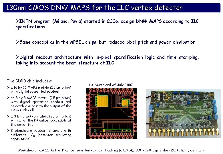
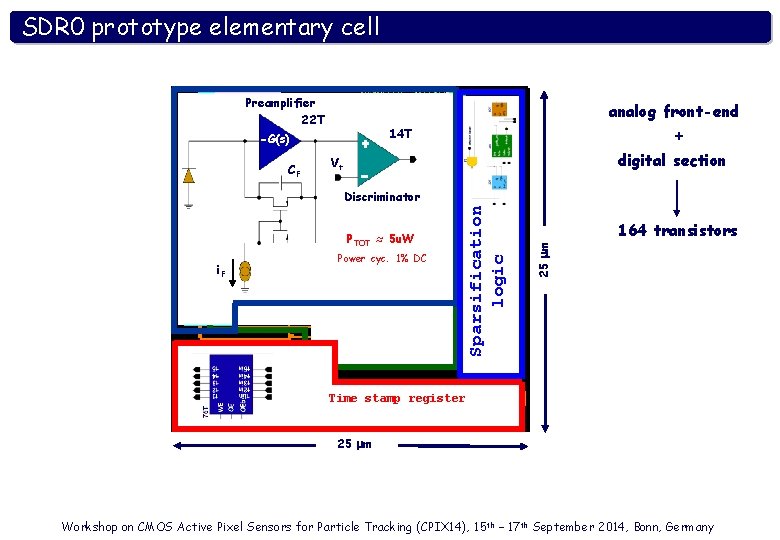
130 nm CMOS DNW MAPS for the ILC vertex detector ØINFN program (Milano, Pavia) started in 2006; design DNW MAPS according to ILC specifications ØSame concept as in the APSEL chips, but reduced pixel pitch and power dissipation ØDigital readout architecture with in-pixel sparsification logic and time stamping, taking into account the beam structure of ILC The SDR 0 chip includes: Ø a 16 by 16 MAPS matrix (25 μm pitch) with digital sparsified readout Delivered end of July 2007 Ø an 8 by 8 MAPS matrix (25 μm pitch) with digital sparsified readout and selectable access to the output of the PA in each cell Ø a 3 by 3 MAPS matrix (25 μm pitch) with all of the PA output accessible at the same time Ø 3 standalone readout channels with different CD (detector simulating capacitance) Workshop on CMOS Active Pixel Sensors for Particle Tracking (CPIX 14), 15 th – 17 th September 2014, Bonn, Germany

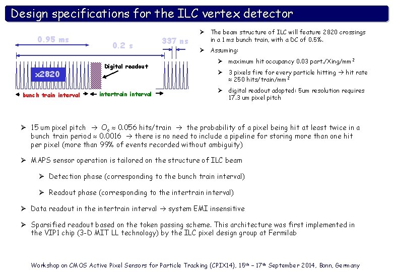
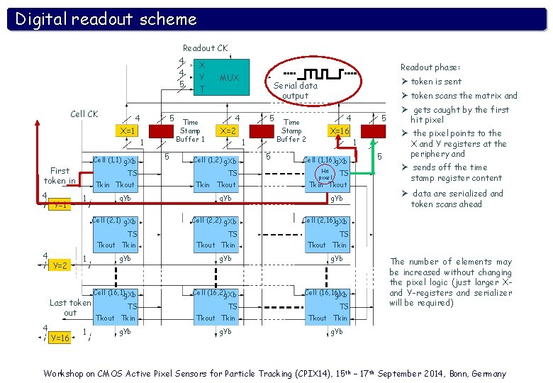
Design specifications for the ILC vertex detector 0. 95 ms x 2820 bunch train interval 0. 2 s Digital readout intertrain interval 337 ns Ø The beam structure of ILC will feature 2820 crossings in a 1 ms bunch train, with a DC of 0. 5%. Ø Assuming: Ø maximum hit occupancy 0. 03 part. /Xing/mm 2 Ø 3 pixels fire for every particle hitting hit rate 250 hits/train/mm 2 Ø digital readout adopted: 5 um resolution requires 17. 3 um pixel pitch Ø 15 um pixel pitch Oc 0. 056 hits/train the probability of a pixel being hit at least twice in a bunch train period 0. 0016 there is no need to include a pipeline for storing more than one hit per pixel (more than 99% of events recorded without ambiguity) Ø MAPS sensor operation is tailored on the structure of ILC beam Ø Detection phase (corresponding to the bunch train interval) Ø Readout phase (corresponding to the intertrain interval) Ø Data readout in the intertrain interval system EMI insensitive Ø Sparsified readout based on the token passing scheme. This architecture was first implemented in the VIP 1 chip (3 -D MIT LL technology) by the ILC pixel design group at Fermilab Workshop on CMOS Active Pixel Sensors for Particle Tracking (CPIX 14), 15 th – 17 th September 2014, Bonn, Germany

SDR 0 prototype elementary cell Preamplifier 22 T analog front-end CF + 14 T -G(s) digital section Vt TOT i. F 164 transistors 25 mm DNW sensor P ≈ 5 u. W Power cyc. 1% DC DNW sensor Sparsification logic Discriminator Time stamp register 25 mm Workshop on CMOS Active Pixel Sensors for Particle Tracking (CPIX 14), 15 th – 17 th September 2014, Bonn, Germany

Digital readout scheme Readout CK 4 X 4 Y MUX 5 T Cell CK 4 X=1 Cell (1, 1) g. Xb First token in 4 4 Y=1 TS Tkin Tkout 1 Y=2 1 Y=16 1 Stamp Buffer 1 1 5 4 X=2 Cell (1, 2) g. Xb TS Tkin Tkout g. Yb Ø token is sent Serial data output 5 1 5 Time Stamp Buffer 2 Ø token scans the matrix and 4 X=16 Cell (1, 16)g. Xb Hit pixel TS Tkin Tkout g. Yb Cell (2, 1) g. Xb Cell (2, 2) g. Xb Cell (2, 16)g. Xb TS TS TS Tkout Tkin Last token out 4 g. Yb 5 Time Readout phase: g. Yb Tkout Tkin g. Yb Cell (16, 2)g. Xb Cell (16, 16) g. Xb TS TS TS g. Yb Tkout Tkin g. Yb Ø gets caught by the first Timehit pixel Stamp Ø the Buffer 16 1 5 pixel points to the X and Y registers at the periphery and g. Xb=get_X_bus Ø sends off the time content g. Yb=get_Y_bus stamp register TS=Time_Stamp Ø data are serialized and Tkin=token_in token scans ahead Tkout=Token_out Tkin Cell (16, 1)g. Xb Tkout Tkin 5 The number of elements may be increased without changing the pixel logic (just larger Xand Y-registers and serializer will be required) Tkout Tkin g. Yb Workshop on CMOS Active Pixel Sensors for Particle Tracking (CPIX 14), 15 th – 17 th September 2014, Bonn, Germany

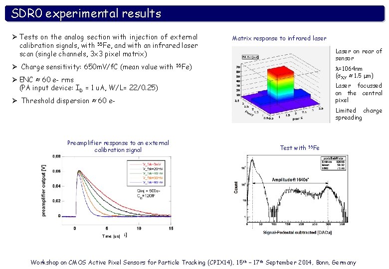
SDR 0 experimental results Ø Tests on the analog section with injection of external calibration signals, with 55 Fe, and with an infrared laser scan (single channels, 3 x 3 pixel matrix) Ø Charge sensitivity: 650 m. V/f. C (mean value with Matrix response to infrared laser Laser on rear of sensor 55 Fe) l=1064 nm (s. XY ≈ 1. 5 mm) Ø ENC ≈ 60 e- rms (PA input device: ID = 1 u. A, W/L= 22/0. 25) Laser focussed on the central pixel Ø Threshold dispersion ≈ 60 e- Limited charge spreading Preamplifier response to an external calibration signal Test with 55 Fe Time [us] Workshop on CMOS Active Pixel Sensors for Particle Tracking (CPIX 14), 15 th – 17 th September 2014, Bonn, Germany

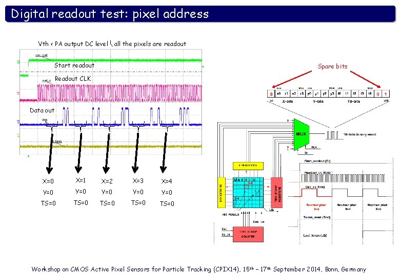
Digital readout test: pixel address Vth < PA output DC level all the pixels are readout Start readout Spare bits Readout CLK Data out X=0 X=1 X=2 X=3 X=4 Y=0 Y=0 Y=0 TS=0 TS=0 Workshop on CMOS Active Pixel Sensors for Particle Tracking (CPIX 14), 15 th – 17 th September 2014, Bonn, Germany

Deep n-well MAPS with 65 nm CMOS IBM technology Workshop on CMOS Active Pixel Sensors for Particle Tracking (CPIX 14), 15 th – 17 th September 2014, Bonn, Germany

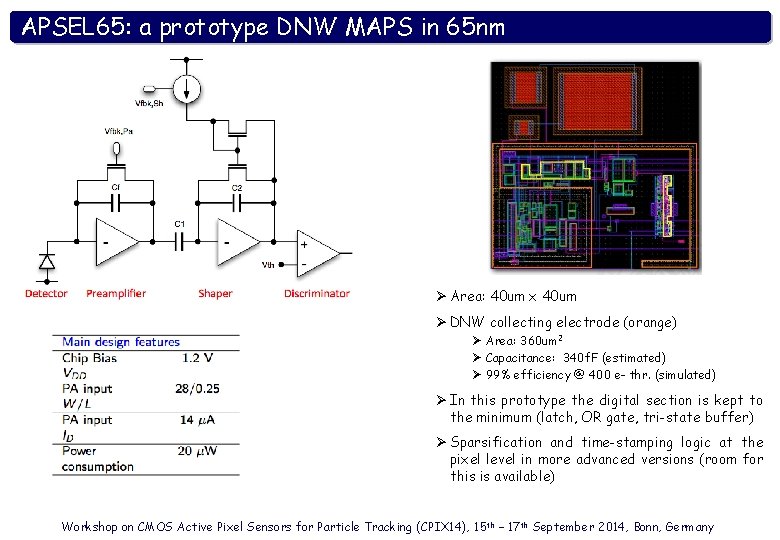
APSEL 65: a prototype DNW MAPS in 65 nm Ø Area: 40 um x 40 um Ø DNW collecting electrode (orange) Ø Area: 360 um 2 Ø Capacitance: 340 f. F (estimated) Ø 99% efficiency @ 400 e- thr. (simulated) Ø In this prototype the digital section is kept to the minimum (latch, OR gate, tri-state buffer) Ø Sparsification and time-stamping logic at the pixel level in more advanced versions (room for this is available) Workshop on CMOS Active Pixel Sensors for Particle Tracking (CPIX 14), 15 th – 17 th September 2014, Bonn, Germany

Deep p-well MAPS with 180 nm CMOS Tower. Jazz technology Workshop on CMOS Active Pixel Sensors for Particle Tracking (CPIX 14), 15 th – 17 th September 2014, Bonn, Germany

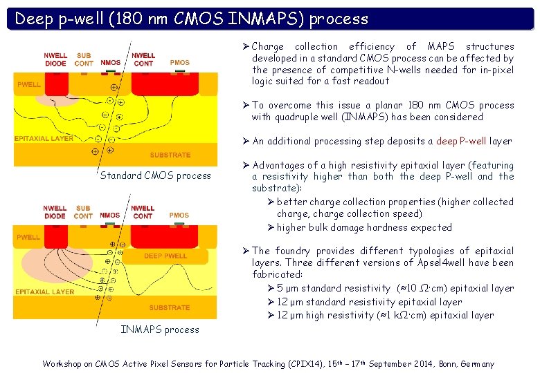
Deep p-well (180 nm CMOS INMAPS) process Ø Charge collection efficiency of MAPS structures developed in a standard CMOS process can be affected by the presence of competitive N-wells needed for in-pixel logic suited for a fast readout Ø To overcome this issue a planar 180 nm CMOS process with quadruple well (INMAPS) has been considered Ø An additional processing step deposits a deep P-well layer Standard CMOS process Ø Advantages of a high resistivity epitaxial layer (featuring a resistivity higher than both the deep P-well and the substrate): Ø better charge collection properties (higher collected charge, charge collection speed) Ø higher bulk damage hardness expected Ø The foundry provides different typologies of epitaxial layers. Three different versions of Apsel 4 well have been fabricated: Ø 5 μm standard resistivity (≈10 Ω∙cm) epitaxial layer Ø 12 μm standard resistivity epitaxial layer Ø 12 μm high resistivity (≈1 kΩ∙cm) epitaxial layer INMAPS process Workshop on CMOS Active Pixel Sensors for Particle Tracking (CPIX 14), 15 th – 17 th September 2014, Bonn, Germany

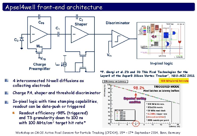
Apsel 4 well front-end architecture *F. Giorgi et al. 2 D “ and 3 D Thin Pixel Technologies for the Layer 0 of the Super. B Silicon Vertex Tracker”, NSS-MIC 2011 4 interconnected N-well diffusions as collecting electrode Charge PA, shaper and threshold discriminator In-pixel logic with time stamping capabilities, readout can be data-push or triggered Readout efficiency >98% (triggered) and TS granularity down to 100 ns with 100 MHz/cm 2 target hit rate* Workshop on CMOS Active Pixel Sensors for Particle Tracking (CPIX 14), 15 th – 17 th September 2014, Bonn, Germany

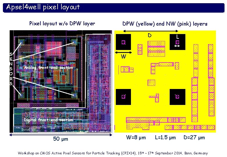
Apsel 4 well pixel layout Pixel layout w/o DPW layer DPW (yellow) and NW (pink) layers D S E N S O R S L W Analog front-end section Digital front-end section 50 μm W=8 μm L=1. 5 μm D=27 μm Workshop on CMOS Active Pixel Sensors for Particle Tracking (CPIX 14), 15 th – 17 th September 2014, Bonn, Germany

Apsel 4 well chip layout Four 3 x 3 test analog matrices: Enclosed layout PA input transistor, 4 collecting electrodes, DPW Open layout PA input transistor, 4 collecting electrodes, DPW EL PA input transistor, 2 collecting electrodes, DPW 5 mm EL PA input transistor, 4 collecting electrodes, no DPW Test structures: Octagonal pn diodes Accumulation capacitors Single analog channels 32 x 32 matrix with peripheral readout logic 5 mm Workshop on CMOS Active Pixel Sensors for Particle Tracking (CPIX 14), 15 th – 17 th September 2014, Bonn, Germany

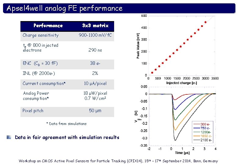
Apsel 4 well analog FE performance Performance 3 x 3 matrix Charge sensitivity 900 -1100 m. V/f. C tp @ 800 injected electrons 290 ns ENC (CD = 30 f. F) 38 e- INL (@ 2000 e-) 2% Current consumption* 10 μA/pixel Analog Power consumption* 18 μW/pixel 0. 7 W/cm 2 Pixel pitch 50 μm * Data from simulations Data in fair agreement with simulation results Workshop on CMOS Active Pixel Sensors for Particle Tracking (CPIX 14), 15 th – 17 th September 2014, Bonn, Germany

Advantages of deep P-well Comparison of charge collection properties performed by means of IR laser N-wells from layout have been superimposed to the charge collection plot No Deep P-well, 5μm std. res. epi layer With deep P-well, 5μm std. res. epi layer 600 In the pixel without DPW the charge is collected only around the electrodes. Workshop on CMOS Active Pixel Sensors for Particle Tracking (CPIX 14), 15 th – 17 th September 2014, Bonn, Germany 400 200 Collected Charge (electrons) 400

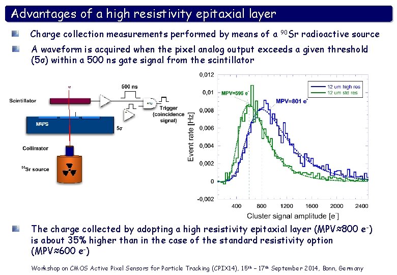
Advantages of a high resistivity epitaxial layer Charge collection measurements performed by means of a 90 Sr radioactive source A waveform is acquired when the pixel analog output exceeds a given threshold (5σ) within a 500 ns gate signal from the scintillator The charge collected by adopting a high resistivity epitaxial layer (MPV≈800 e -) is about 35% higher than in the case of the standard resistivity option (MPV≈600 e-) Workshop on CMOS Active Pixel Sensors for Particle Tracking (CPIX 14), 15 th – 17 th September 2014, Bonn, Germany

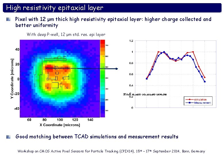
High resistivity epitaxial layer Pixel with 12 μm thick high resistivity epitaxial layer: higher charge collected and better uniformity With deep P-well, 12 μm std. res. epi layer With deep P-well, 5 μm std. res. epi layer Good matching between TCAD simulations and measurement results Workshop on CMOS Active Pixel Sensors for Particle Tracking (CPIX 14), 15 th – 17 th September 2014, Bonn, Germany Collected Charge (electrons) 400

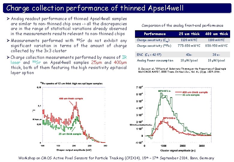
Charge collection performance of thinned Apsel 4 well Ø Analog readout performance of thinned Apsel 4 well samples are similar to non-thinned chip ones -> all the discrepancies are in the range of statistical variations already observed in the measurements results relevant to non-thinned chips Ø Measurements performed with 90 Sr do not exhibit any significant variation in terms of the amount of charge collected by the 3 x 3 cluster Ø Charge collection measurements performed by means of IR laser and 90 Sr on Apsel 4 well samples 25μm and 400μm thick, both of them featuring the high resistivity epitaxial layer option Comparison of the analog front-end performance Performance 25 um thick 400 um thick Charge sensitivity (Cinj) 1120 m. V/f. C 1100 m. V/f. C Charge sensitivity (55 Fe) 775 -850 m. V/f. C 850 -950 m. V/f. C 43 e- 38 e- 18 μW/pixel ENC (CT = 42 f. F) Analog Power consumption S. Zucca et al. , “Effects of Substrate Thinning on the Properties of Quadruple Well CMOS MAPS”, IEEE Trans. On Nucl. Sci. , Vol. 61, (2) pp. 1039 -1046. Workshop on CMOS Active Pixel Sensors for Particle Tracking (CPIX 14), 15 th – 17 th September 2014, Bonn, Germany

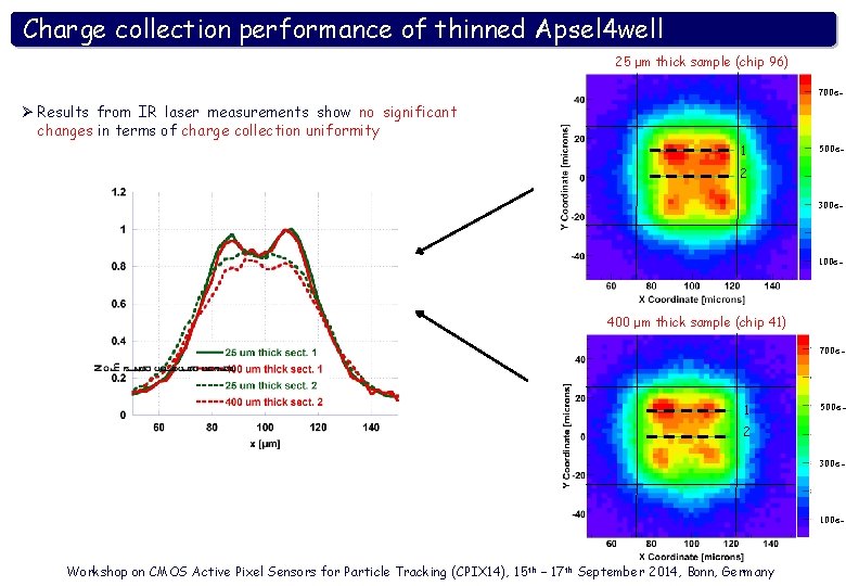
Charge collection performance of thinned Apsel 4 well 25 μm thick sample (chip 96) 700 e- Ø Results from IR laser measurements show no significant changes in terms of charge collection uniformity 1 500 e- 2 300 e- 100 e- 400 μm thick sample (chip 41) 700 e- 1 500 e- 2 300 e- 100 e- Workshop on CMOS Active Pixel Sensors for Particle Tracking (CPIX 14), 15 th – 17 th September 2014, Bonn, Germany

Conclusions Ø Several deep n-well MAPS chip have been fabricated and tested with the 130 nm CMOS ST technology Ø APSEL 4 D (4096 pixels, 50 um pitch) featuring in-pixel sparsification and time-stamp information has been characterized in laboratory and tested with beams Ø SDR 0, a monolithic active pixel sensor for vertexing applications at the ILC has been fabricated and tested. Several issues (pitch, digital functionality, detection efficiency) had to be addressed in order to meet the ILC requirement -> SDR 1 in 3 D Tezzaron-Global. Foundries process Ø A test chip including deep n-well MAPS has been fabricated and tested in the 65 nm CMOS IBM process Ø MAPS devices developed in the 180 nm CMOS INMAPS process (deep p-well) can significantly improve the charge collection efficiency of DNW MAPS by preventing the parasitic collection action of n-well diffusions Ø The high resistivity epitaxial layer option improves both the charge collection properties of the sensor and its bulk damage tolerance Ø APSEL 4 WELL sensor was fully characterized by means of charge injection, infrared laser scan and radiation sources Ø Sensors fabricated in a 12 um thick HR epi layer have been proven to be by far the best solution among the different available options in terms both of the amount of collected charge and of charge collection uniformity Ø APSEL 4 WELL MAPS thinned down to about 25 um have been tested and no significant changes in the performance of the thinned sensors have been detected with respect to non-thinned chips Workshop on CMOS Active Pixel Sensors for Particle Tracking (CPIX 14), 15 th – 17 th September 2014, Bonn, Germany

Acknowledgments Ø L. Gaioni, M. Manghisoni, V. Re Università di Bergamo and INFN Pavia Ø G. Bruni, M. Bruschi, R. Di Sipio, B. Giacobbe, F. M. Giorgi, A. Gabrielli, C. Sbarra, N. Semprini, M. Villa, A. Zoccoli Università di Bologna and INFN Bologna Ø M. Caccia, A. Bulgheroni, F. Risigo, M. Jastrzab Università dell’Insubria e INFN Milano Ø L. Ratti, A. Manazza, V. Speziali, S. Zucca, E. Pozzati, C. Andreoli Università di Pavia and INFN Pavia Ø G. Batignani, S. Bettarini, G. Casarosa, M. Dell’Orso, F. Forti, P. Giannetti, M. A. Giorgi, F. Morsani, N. Neri, E. Paoloni, M. Piendibene, G. Rizzo Università di Pisa and INFN Pisa Ø L. Bissi, P. Ciampolini, A. Marras, G. Matrella, P. Placidi, E. Pilicer, D. Passeri, L. Servoli, P. Tucceri Università di Perugia and INFN Perugia Ø E. Bernieri, G. Conte, M. C. Rossi, G. Assanto, L. Colace, E. Spiriti INFN Roma III Ø G. F. Dalla Betta, A. Repchankova, V. Tyzhnevyi, G. Verzellesi Università di Trento and TIFPA INFN Ø L. Bosisio, L. Lanceri, L. Vitale, I. Rashevskaya Università di Trieste and INFN Trieste Ø R. Yarema, F. Fahim, G. Deptuch, T. Zimmerman, A. Shenai, J. Hoff, M. Trimpl Fermi National Accelator Laboratory Ø R. Turchetta, J. Crooks, R. Coath Rutherford Appleton Laboratory Workshop on CMOS Active Pixel Sensors for Particle Tracking (CPIX 14), 15 th – 17 th September 2014, Bonn, Germany

Backup slides Workshop on CMOS Active Pixel Sensors for Particle Tracking (CPIX 14), 15 th – 17 th September 2014, Bonn, Germany

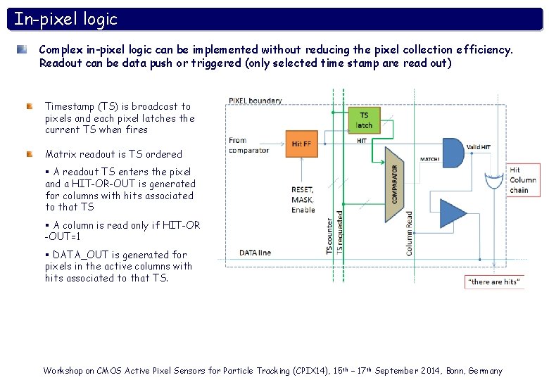
In-pixel logic Complex in-pixel logic can be implemented without reducing the pixel collection efficiency. Readout can be data push or triggered (only selected time stamp are read out) Timestamp (TS) is broadcast to pixels and each pixel latches the current TS when fires Matrix readout is TS ordered § A readout TS enters the pixel and a HIT-OR-OUT is generated for columns with hits associated to that TS § A column is read only if HIT-OR -OUT=1 § DATA_OUT is generated for pixels in the active columns with hits associated to that TS. Workshop on CMOS Active Pixel Sensors for Particle Tracking (CPIX 14), 15 th – 17 th September 2014, Bonn, Germany

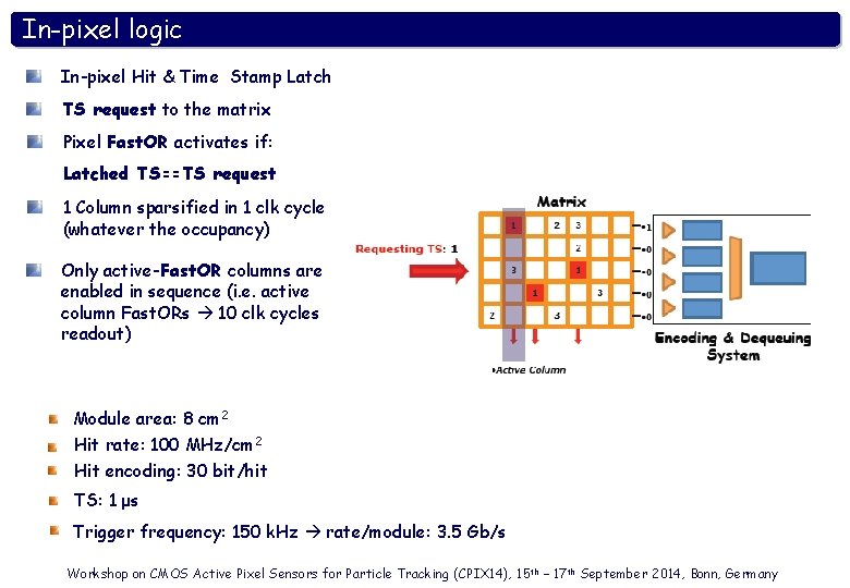
In-pixel logic In-pixel Hit & Time Stamp Latch TS request to the matrix Pixel Fast. OR activates if: Latched TS==TS request 1 Column sparsified in 1 clk cycle (whatever the occupancy) Only active-Fast. OR columns are enabled in sequence (i. e. active column Fast. ORs 10 clk cycles readout) Module area: 8 cm 2 Hit rate: 100 MHz/cm 2 Hit encoding: 30 bit/hit TS: 1 μs Trigger frequency: 150 k. Hz rate/module: 3. 5 Gb/s Workshop on CMOS Active Pixel Sensors for Particle Tracking (CPIX 14), 15 th – 17 th September 2014, Bonn, Germany

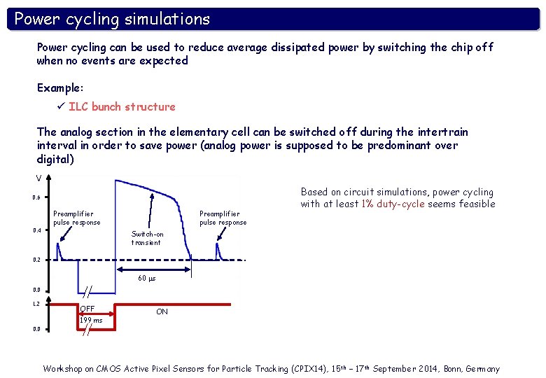
Power cycling simulations Power cycling can be used to reduce average dissipated power by switching the chip off when no events are expected Example: ü ILC bunch structure: ~330 ns spacing, ~3000 bunches, 5 Hz pulse The analog section in the elementary cell can be switched off during the intertrain interval in order to save power (analog power is supposed to be predominant over digital) V 0. 6 0. 4 Preamplifier pulse response Based on circuit simulations, power cycling with at least 1% duty-cycle seems feasible Switch-on transient 0. 2 60 ms 0. 0 1. 2 0. 0 OFF 199 ms ON Workshop on CMOS Active Pixel Sensors for Particle Tracking (CPIX 14), 15 th – 17 th September 2014, Bonn, Germany