Applications of PPI AD Temperature Sensor Analog to


")

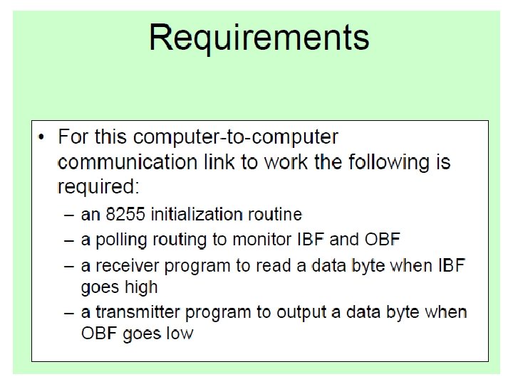
")
")
.")
")

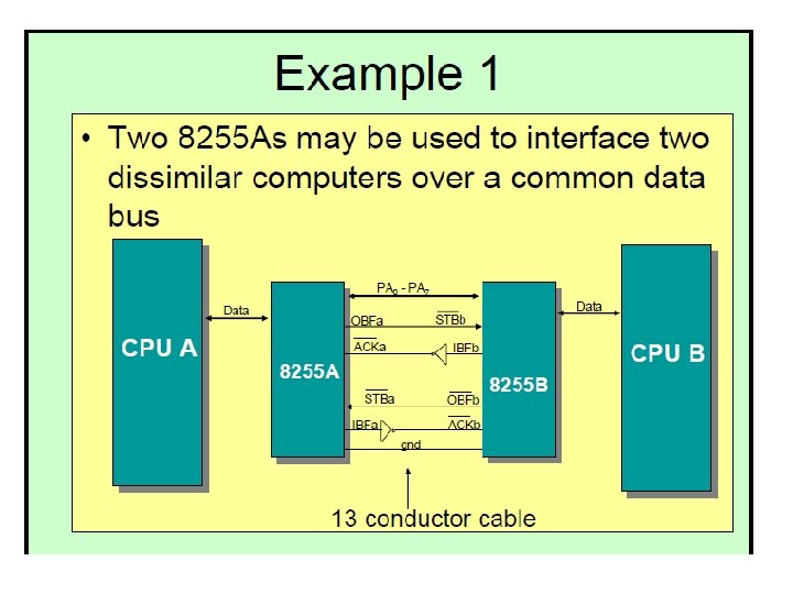
. The OBF output")
- Slides: 27
Applications of PPI A/D - Temperature Sensor
Analog to Digital
Vin Range
Timing
Interfacing ADC
Example
Temperature Sensor LM 34 Datasheet
Handshaking IO Example Printer Connection
IO Base Address for LPT
LPT Adresses
Printer’s Ports
8255 Mode Definition Summary
Mode 0 • Provides simple input and output operations for each of the three ports. – No “handshaking” is required, data is simply written to or read from a specified port. – Two 8 -bit ports and two 4 -bit ports. – Any port can be input or output. – Outputs are latched. – Inputs are not latched
• Mode 1 Basic functional Definitions: – – Two Groups (Group A and Group B). Each group has one 8 -bit data port and one 4 -bit control/data port. The 8 -bit data port can be either input or output. Both inputs and outputs are latched. The 4 -bit port is used for control and status of the 8 -bit data port.
8255 mode 1 (output)
Mode 1 – Control Signals • Output Control Signal Definition – OBF (Output Buffer Full F/F). (C 7 for A, C 1 for B) • The OBF output will go “low” to indicate that the CPU has written data out to the specified port. – A signal to the device that there is data to be read. – ACK (Acknowledge Input). (C 6 for A, C 2 for B) • A “low” on this input informs the 8255 that the data from Port A or Port B has been accepted. – A response from the peripheral device indicating that it has read the data. – INTR (Interrupt Request). (C 3 for A, C 0 for B) • A “high” on this output can be used to interrupt the CPU when an output device has accepted data transmitted by the CPU.
Timing diagram for mode 1(output)
8255 mode 1 (input)
Mode 1 – Control Signals • Input Control Signal Definition – STB (Strobe Input). (C 4 for A, C 2 for B) • A “low” on this input loads data into the input latch. – IBF (Input Buffer Full F/F) (C 5 for A, C 1 for B) • A “high” on this output indicates that the data has been loaded into the input latch; in essence, an acknowledgement from the 8255 to the device. – INTR (Interrupt Request) (C 3 for A, C 0 for B) • A “high” on this output can be used to interrupt the CPU when an input device is requesting service.
Timing diagram for mode 1(input)
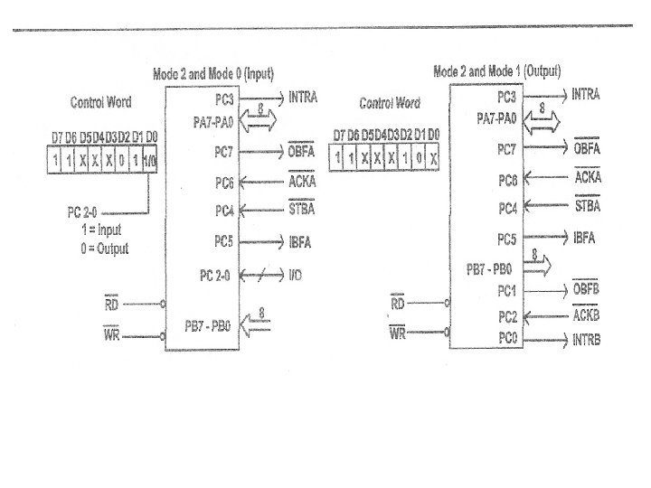
• MODE 2 Basic Functional Definitions: – – Used in Group A only. One 8 -bit, bi-directional bus port (Port A) and a 5 -bit control port (Port C). Both inputs and outputs are latched. The 5 -bit control port (Port C) is used for control and status for the 8 -bit, bi-directional bus port (Port A).
• Output Operations Mode 2 – OBF (Output Buffer Full). The OBF output will go low to indicate that the CPU has written data out to port A. – ACK (Acknowledge). A low on this input enables the tri-state output buffer of Port A to send out the data. Otherwise, the output buffer will be in the high impedance state. • Input Operations – STB (Strobe Input). A low on this input loads data into the input latch. – IBF (Input Buffer Full F/F). A high on this output indicates that data has been loaded into the input latch. Pin Function PC 7 /OBF PC 6 /ACK PC 5 IBF PC 4 /STB PC 3 INTR PC 2 I/O PC 1 I/O PC 0 I/O