Application of Vertically Integrated Electronics and Sensors 3
- Slides: 27

Application of Vertically Integrated Electronics and Sensors (3 D) to Track Triggers Contents • Overview of 3 D • Fermilab Developments • Sensor integration using oxide bonding • Tezzaron 3 D Run • Application to the CMS s. LHC Trigger Module • Conclusions Ronald Lipton, ACES March 4, 2009 1

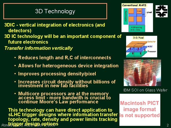
3 D Technology 3 DIC - vertical integration of electronics (and detectors) 3 D IC technology will be an important component of future electronics Transfer information vertically • Reduces length and R, C of interconnects • Allows for heterogeneous device integration • Improves processing density/pixel • Increases circuit density without billions of investment in new fab facilities • Multicore processors are at the memory access limit - more bandwith is crucial to continue Moore’s Law performance This technology can have direct application to s. LHC trigger designs where information transfer topology, rate, density and power limits tracking trigger design Ronald Lipton, ACES Marchoptions 4, 2009 IBM SOI on Glass Wafer Tezzaron 3 D FPGA 2

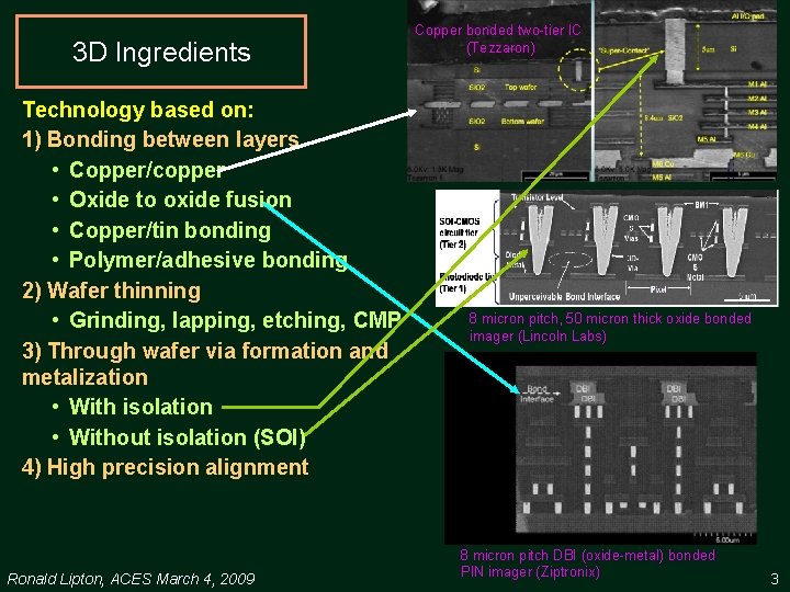
3 D Ingredients Technology based on: 1) Bonding between layers • Copper/copper • Oxide to oxide fusion • Copper/tin bonding • Polymer/adhesive bonding 2) Wafer thinning • Grinding, lapping, etching, CMP 3) Through wafer via formation and metalization • With isolation • Without isolation (SOI) 4) High precision alignment Ronald Lipton, ACES March 4, 2009 Copper bonded two-tier IC (Tezzaron) 8 micron pitch, 50 micron thick oxide bonded imager (Lincoln Labs) 8 micron pitch DBI (oxide-metal) bonded PIN imager (Ziptronix) 3

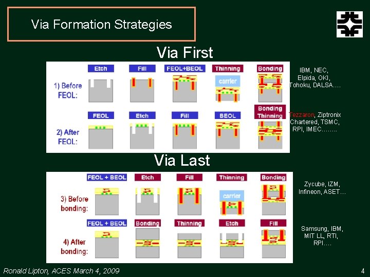
Via Formation Strategies Via First IBM, NEC, Elpida, OKI, Tohoku, DALSA…. Tezzaron, Ziptronix Chartered, TSMC, RPI, IMEC……. . Via Last Zycube, IZM, Infineon, ASET… Samsung, IBM, MIT LL, RTI, RPI…. Ronald Lipton, ACES March 4, 2009 4

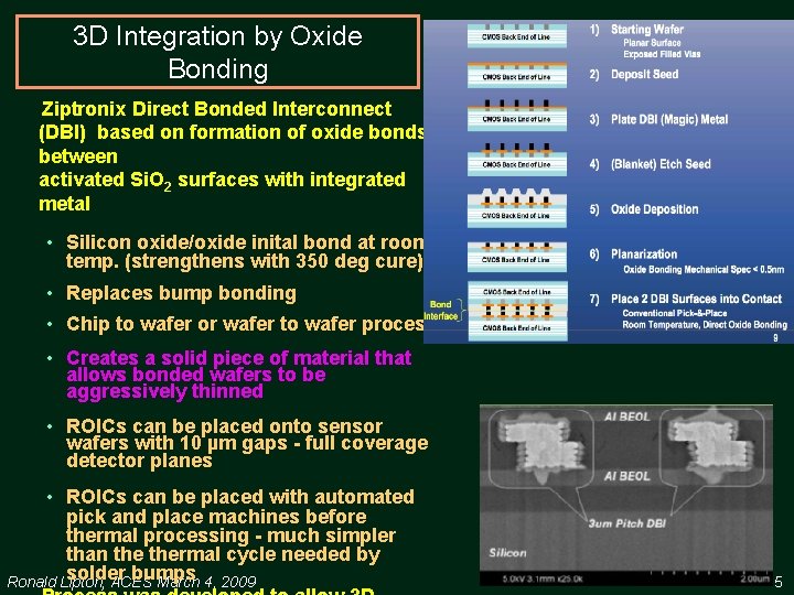
3 D Integration by Oxide Bonding Ziptronix Direct Bonded Interconnect (DBI) based on formation of oxide bonds between activated Si. O 2 surfaces with integrated metal • Silicon oxide/oxide inital bond at room temp. (strengthens with 350 deg cure) • Replaces bump bonding • Chip to wafer or wafer to wafer process • Creates a solid piece of material that allows bonded wafers to be aggressively thinned • ROICs can be placed onto sensor wafers with 10 µm gaps - full coverage detector planes • ROICs can be placed with automated pick and place machines before thermal processing - much simpler than thermal cycle needed by solder bumps Ronald Lipton, ACES March 4, 2009 5

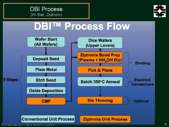
DBI Process (W. Bair, Ziptronix) Ronald Lipton, ACES March 4, 2009 6

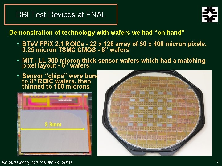
DBI Test Devices at FNAL Demonstration of technology with wafers we had “on hand” • BTe. V FPi. X 2. 1 ROICs - 22 x 128 array of 50 x 400 micron pixels. 0. 25 micron TSMC CMOS - 8” wafers • MIT - LL 300 micron thick sensor wafers which had a matching pixel layout - 6” wafers • Sensor “chips” were bonded to 8” ROIC wafers, then thinned to 100 microns 9. 9 mm Ronald Lipton, ACES March 4, 2009 7

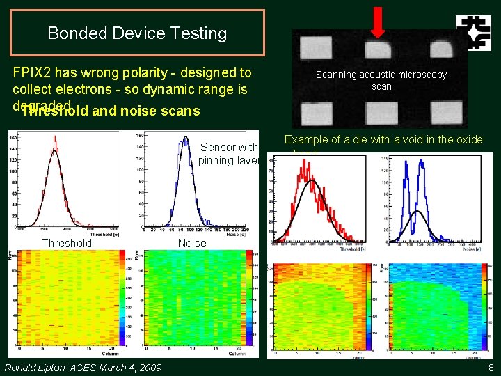
Bonded Device Testing FPIX 2 has wrong polarity - designed to collect electrons - so dynamic range is degraded Threshold and noise scans Sensor with pinning layer Threshold Scanning acoustic microscopy scan Example of a die with a void in the oxide bond Noise Threshold Ronald Lipton, ACES March 4, 2009 Noise 8

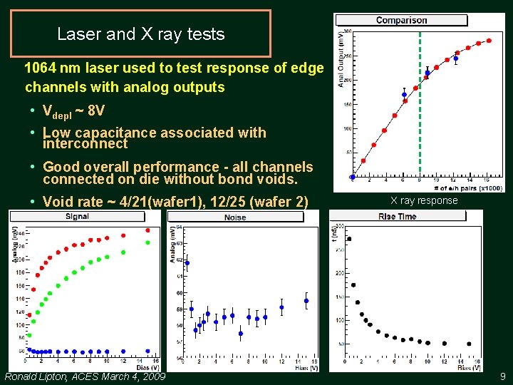
Laser and X ray tests 1064 nm laser used to test response of edge channels with analog outputs • Vdepl ~ 8 V • Low capacitance associated with interconnect • Good overall performance - all channels connected on die without bond voids. • Void rate ~ 4/21(wafer 1), 12/25 (wafer 2) Ronald Lipton, ACES March 4, 2009 X ray response 9

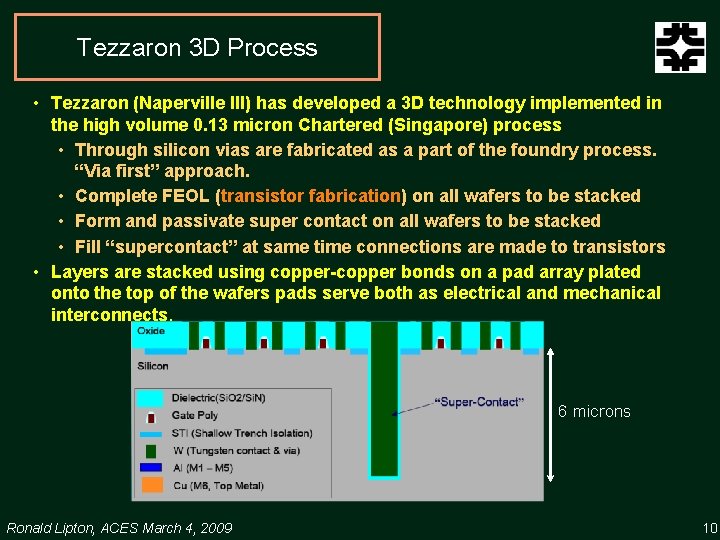
Tezzaron 3 D Process • Tezzaron (Naperville Ill) has developed a 3 D technology implemented in the high volume 0. 13 micron Chartered (Singapore) process • Through silicon vias are fabricated as a part of the foundry process. “Via first” approach. • Complete FEOL (transistor fabrication) on all wafers to be stacked • Form and passivate super contact on all wafers to be stacked • Fill “supercontact” at same time connections are made to transistors • Layers are stacked using copper-copper bonds on a pad array plated onto the top of the wafers pads serve both as electrical and mechanical interconnects. 6 microns Ronald Lipton, ACES March 4, 2009 10

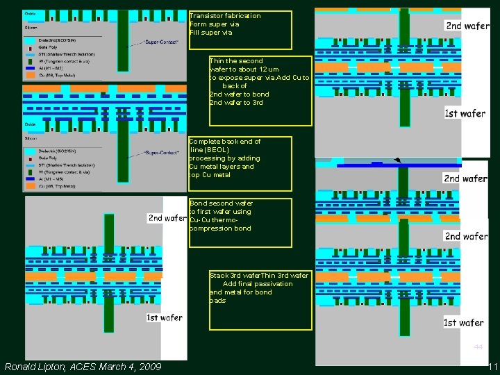
Transistor fabrication Form super via Fill super via Thin the second wafer to about 12 um to expose super via. Add Cu to back of 2 nd wafer to bond 2 nd wafer to 3 rd Complete back end of line (BEOL) processing by adding Cu metal layers and top Cu metal Bond second wafer to first wafer using Cu-Cu thermocompression bond Stack 3 rd wafer. Thin 3 rd wafer Add final passivation and metal for bond pads 44 Ronald Lipton, ACES March 4, 2009 11

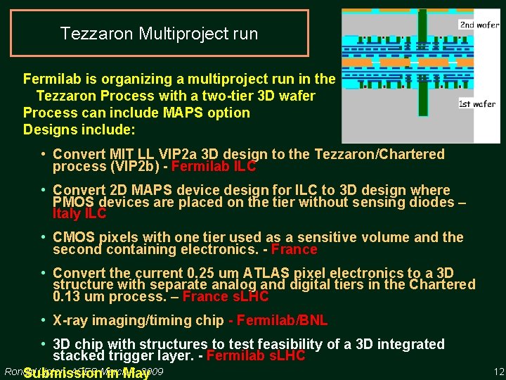
Tezzaron Multiproject run Fermilab is organizing a multiproject run in the Tezzaron Process with a two-tier 3 D wafer Process can include MAPS option Designs include: • Convert MIT LL VIP 2 a 3 D design to the Tezzaron/Chartered process (VIP 2 b) - Fermilab ILC • Convert 2 D MAPS device design for ILC to 3 D design where PMOS devices are placed on the tier without sensing diodes – Italy ILC • CMOS pixels with one tier used as a sensitive volume and the second containing electronics. - France • Convert the current 0. 25 um ATLAS pixel electronics to a 3 D structure with separate analog and digital tiers in the Chartered 0. 13 um process. – France s. LHC • X-ray imaging/timing chip - Fermilab/BNL • 3 D chip with structures to test feasibility of a 3 D integrated stacked trigger layer. - Fermilab s. LHC Ronald Lipton, ACES March 4, 2009 Submission in May 12

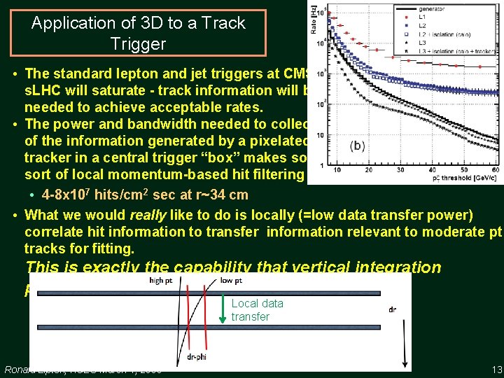
Application of 3 D to a Track Trigger • The standard lepton and jet triggers at CMS in s. LHC will saturate - track information will be needed to achieve acceptable rates. • The power and bandwidth needed to collect all of the information generated by a pixelated tracker in a central trigger “box” makes some sort of local momentum-based hit filtering crucial • 4 -8 x 10⁷ hits/cm 2 sec at r~34 cm • What we would really like to do is locally (=low data transfer power) correlate hit information to transfer information relevant to moderate pt tracks for fitting. This is exactly the capability that vertical integration provides Local data transfer Ronald Lipton, ACES March 4, 2009 13

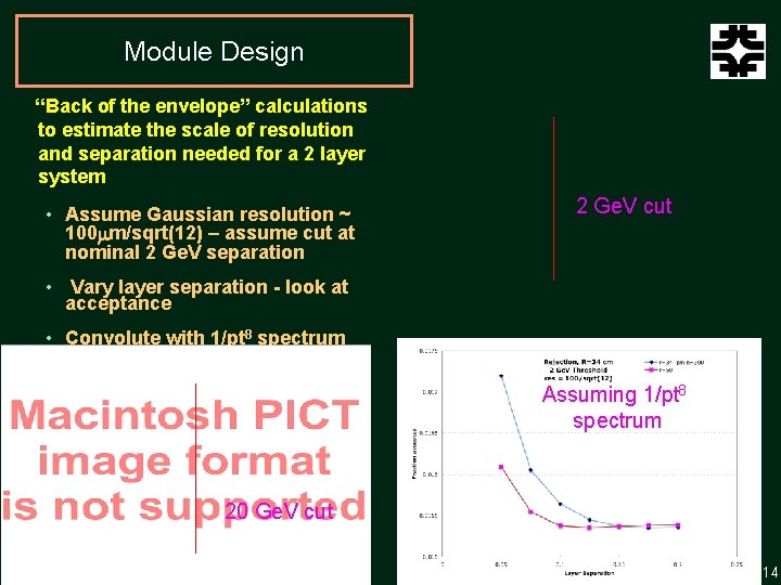
Module Design “Back of the envelope” calculations to estimate the scale of resolution and separation needed for a 2 layer system • Assume Gaussian resolution ~ 100 mm/sqrt(12) – assume cut at nominal 2 Ge. V separation 2 Ge. V cut • Vary layer separation - look at acceptance • Convolute with 1/pt 8 spectrum Assuming 1/pt 8 spectrum 20 Ge. V cut Ronald Lipton, ACES March 4, 2009 14

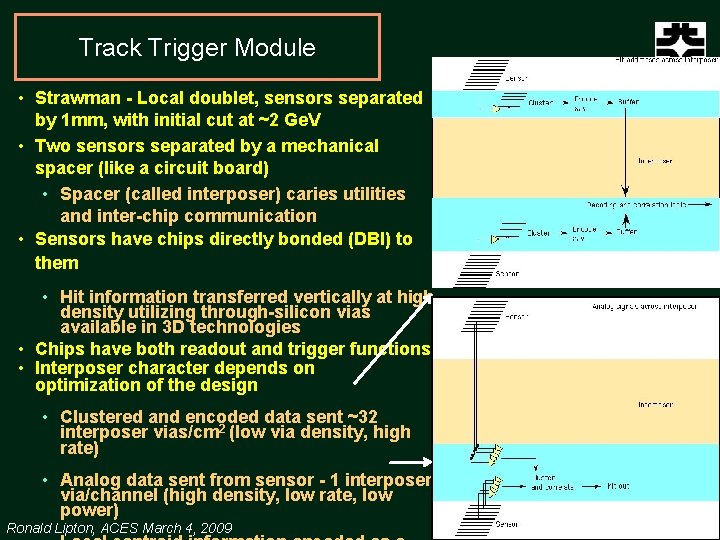
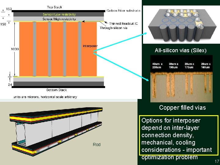
Track Trigger Module • Strawman - Local doublet, sensors separated by 1 mm, with initial cut at ~2 Ge. V • Two sensors separated by a mechanical spacer (like a circuit board) • Spacer (called interposer) caries utilities and inter-chip communication • Sensors have chips directly bonded (DBI) to them • Hit information transferred vertically at high density utilizing through-silicon vias available in 3 D technologies • Chips have both readout and trigger functions • Interposer character depends on optimization of the design • Clustered and encoded data sent ~32 interposer vias/cm 2 (low via density, high rate) • Analog data sent from sensor - 1 interposer via/channel (high density, low rate, low power) Ronald Lipton, ACES March 4, 2009 15

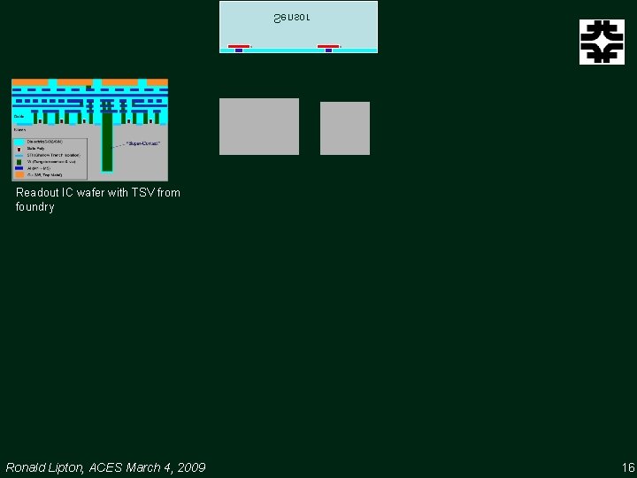
Sensor Readout IC wafer with TSV from foundry Ronald Lipton, ACES March 4, 2009 16

Module Structure All-silicon vias (Silex) Copper filled vias Rod Ronald Lipton, ACES March 4, 2009 Options for interposer depend on inter-layer connection density, mechanical, cooling considerations - important optimization problem 17

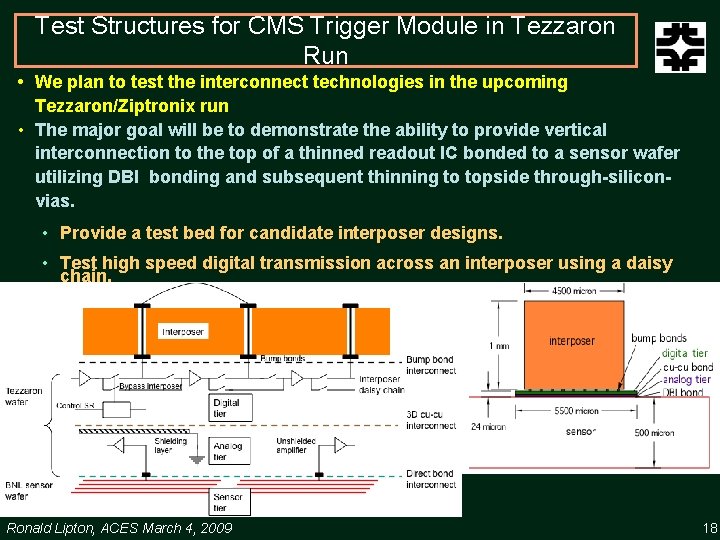
Test Structures for CMS Trigger Module in Tezzaron Run • We plan to test the interconnect technologies in the upcoming Tezzaron/Ziptronix run • The major goal will be to demonstrate the ability to provide vertical interconnection to the top of a thinned readout IC bonded to a sensor wafer utilizing DBI bonding and subsequent thinning to topside through-siliconvias. • Provide a test bed for candidate interposer designs. • Test high speed digital transmission across an interposer using a daisy chain. • Test digital-to-analog crosstalk using amplifiers connected to a sensor tier • Include structures to test design options for data transmission Ronald Lipton, ACES March 4, 2009 18

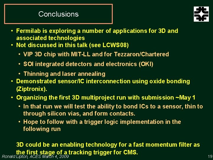
Conclusions • Fermilab is exploring a number of applications for 3 D and associated technologies • Not discussed in this talk (see LCWS 08) • VIP 3 D chip with MIT-LL and for Tezzaron/Chartered • SOI integrated detectors and electronics (OKI) • Thinning and laser annealing • Demonstrated sensor/IC interconnection using oxide bonding (Ziptronix). • Organizing the first 3 D multiproject run with submission ~May 1 • In that run we will test the ability to bond ICs to a sensor, thin to through silicon vias, and form contacts. • Hope to follow with a trigger logic implementation in the following run 3 D could be an enabling technology for a fast momentum filter as the first stage of a tracking trigger for CMS. Ronald Lipton, ACES March 4, 2009 19

Extras Ronald Lipton, ACES March 4, 2009 20

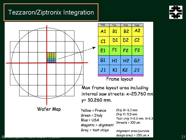
Tezzaron/Ziptronix Integration Use single wafer with mirrored circuits to generate a two-tier circuit on ½ of the reticle Sensor wafer for Ziptronix Central region – contact TSV Outer region – redistribution of contacts to pads Ronald Lipton, ACES March 4, 2009 21

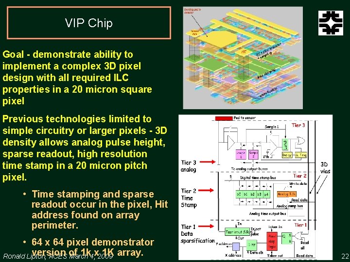
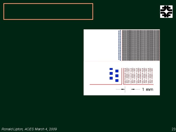
VIP Chip Goal - demonstrate ability to implement a complex 3 D pixel design with all required ILC properties in a 20 micron square pixel Previous technologies limited to simple circuitry or larger pixels - 3 D density allows analog pulse height, sparse readout, high resolution time stamp in a 20 micron pitch pixel. • Time stamping and sparse readout occur in the pixel, Hit address found on array perimeter. • 64 x 64 pixel demonstrator version 1 k 4, x 2009 1 K array. Ronald Lipton, ACES of March 22

Ronald Lipton, ACES March 4, 2009 23

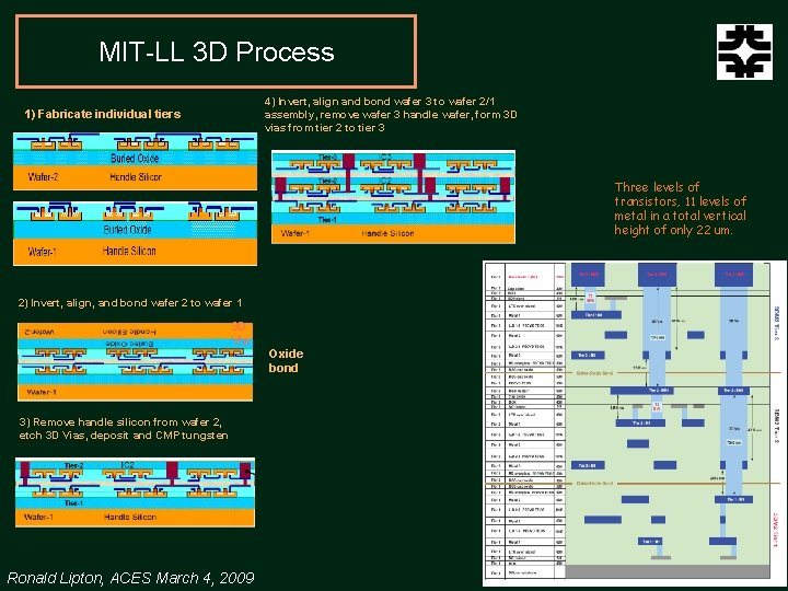
MIT-LL 3 D Process 4) Invert, align and bond wafer 3 to wafer 2/1 assembly, remove wafer 3 handle wafer, form 3 D vias from tier 2 to tier 3 1) Fabricate individual tiers Three levels of transistors, 11 levels of metal in a total vertical height of only 22 um. 2) Invert, align, and bond wafer 2 to wafer 1 3 D Via Oxide bond 3) Remove handle silicon from wafer 2, etch 3 D Vias, deposit and CMP tungsten Ronald Lipton, ACES March 4, 2009 24

VIP Test results Basic functionality of the chip has been demonstrated • Propagation of readout token • Threshold scan • Input test charge scan • Digital and analog time stamping • Full sparsified data readout No problems could be found associated with the 3 D vias between tiers. Chip performance compromised by SOI issues: • Large leakage currents in transistors and diodes • Poor current mirror matching, Vdd sensitivity, low yield An improved version of the VIP was submitted to MIT LL in October. The new chip is called VIP 2 • More conservative design, larger features - less dependence on dynamic logic, pixel size 20 ->30 microns Ronald Lipton, ACES March 4, 2009 25

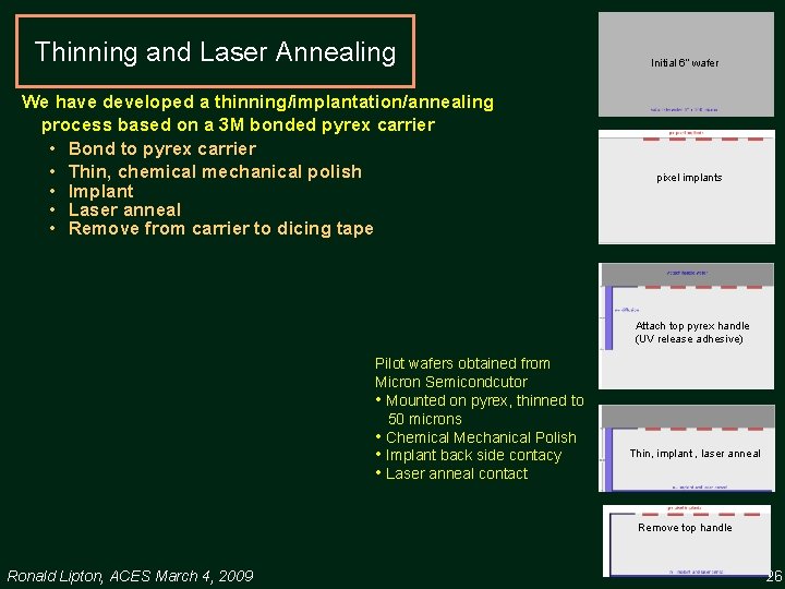
Thinning and Laser Annealing We have developed a thinning/implantation/annealing process based on a 3 M bonded pyrex carrier • Bond to pyrex carrier • Thin, chemical mechanical polish • Implant • Laser anneal • Remove from carrier to dicing tape Initial 6” wafer pixel implants Attach top pyrex handle (UV release adhesive) Pilot wafers obtained from Micron Semicondcutor • Mounted on pyrex, thinned to 50 microns • Chemical Mechanical Polish • Implant back side contacy • Laser anneal contact Thin, implant , laser anneal Remove top handle Ronald Lipton, ACES March 4, 2009 26

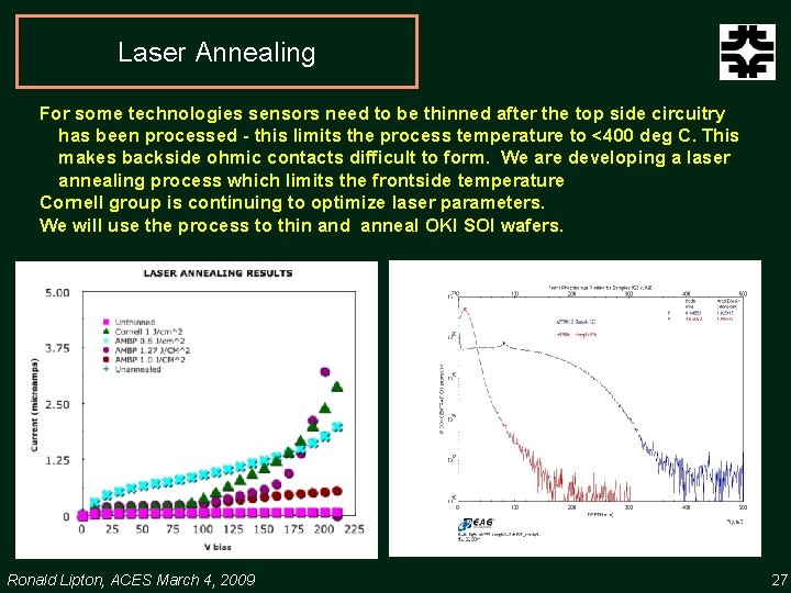
Laser Annealing For some technologies sensors need to be thinned after the top side circuitry has been processed - this limits the process temperature to <400 deg C. This makes backside ohmic contacts difficult to form. We are developing a laser annealing process which limits the frontside temperature Cornell group is continuing to optimize laser parameters. We will use the process to thin and anneal OKI SOI wafers. Ronald Lipton, ACES March 4, 2009 27