Appendix E Authors John Hennessy David Patterson Copyright
- Slides: 12

Appendix E Authors: John Hennessy & David Patterson Copyright © 2011, Elsevier Inc. All rights Reserved. 1

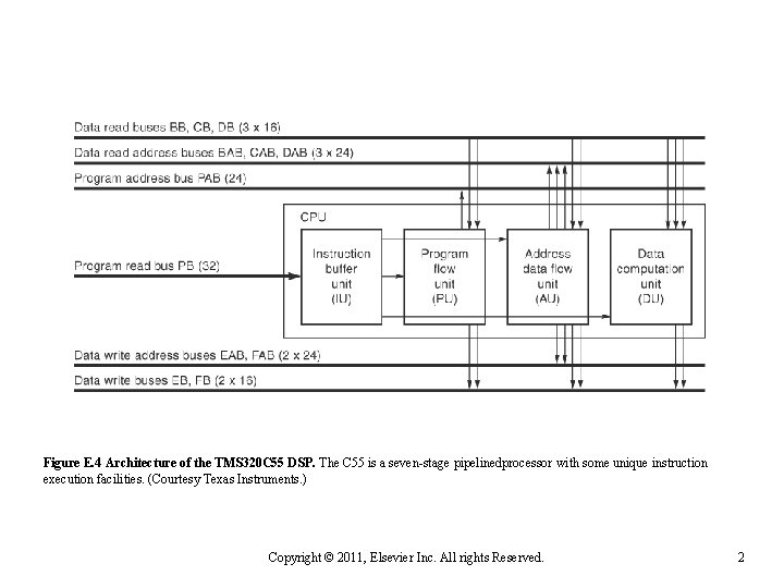
Figure E. 4 Architecture of the TMS 320 C 55 DSP. The C 55 is a seven-stage pipelinedprocessor with some unique instruction execution facilities. (Courtesy Texas Instruments. ) Copyright © 2011, Elsevier Inc. All rights Reserved. 2

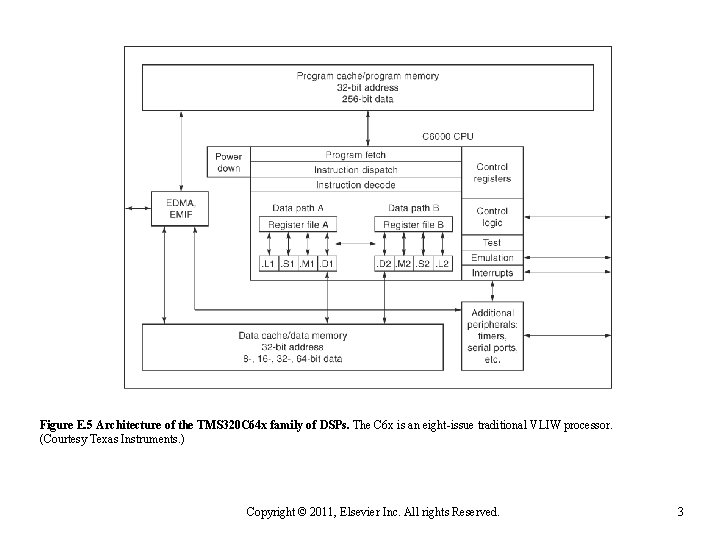
Figure E. 5 Architecture of the TMS 320 C 64 x family of DSPs. The C 6 x is an eight-issue traditional VLIW processor. (Courtesy Texas Instruments. ) Copyright © 2011, Elsevier Inc. All rights Reserved. 3

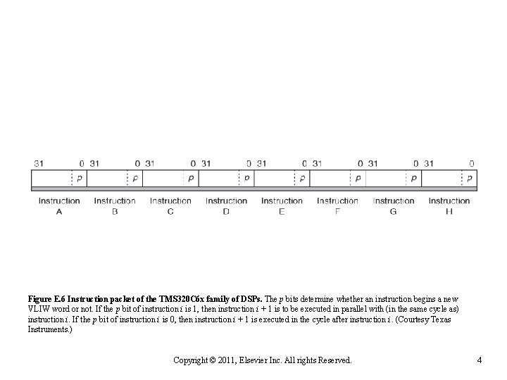
Figure E. 6 Instruction packet of the TMS 320 C 6 x family of DSPs. The p bits determine whether an instruction begins a new VLIW word or not. If the p bit of instruction i is 1, then instruction i + 1 is to be executed in parallel with (in the same cycle as) instruction i. If the p bit of instruction i is 0, then instruction i + 1 is executed in the cycle after instruction i. (Courtesy Texas Instruments. ) Copyright © 2011, Elsevier Inc. All rights Reserved. 4

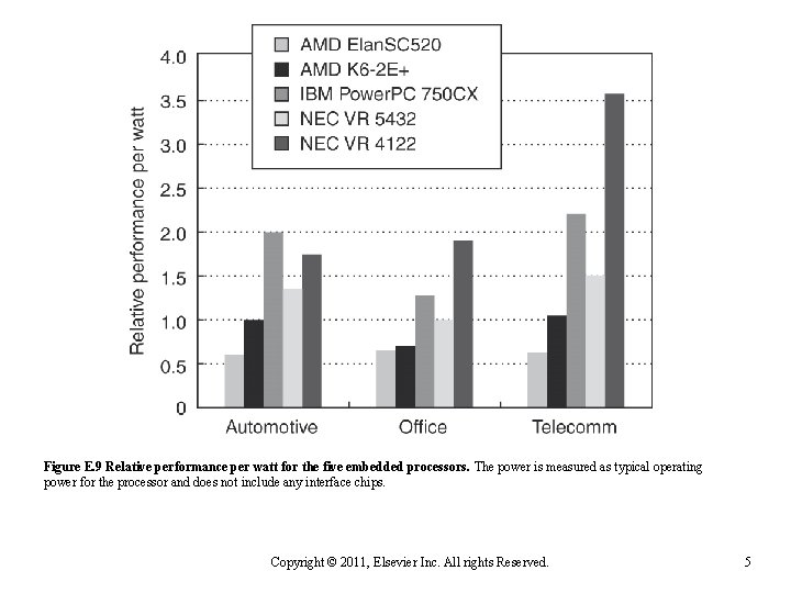
Figure E. 9 Relative performance per watt for the five embedded processors. The power is measured as typical operating power for the processor and does not include any interface chips. Copyright © 2011, Elsevier Inc. All rights Reserved. 5

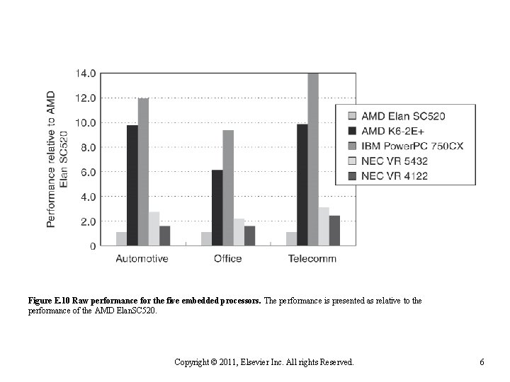
Figure E. 10 Raw performance for the five embedded processors. The performance is presented as relative to the performance of the AMD Elan. SC 520. Copyright © 2011, Elsevier Inc. All rights Reserved. 6

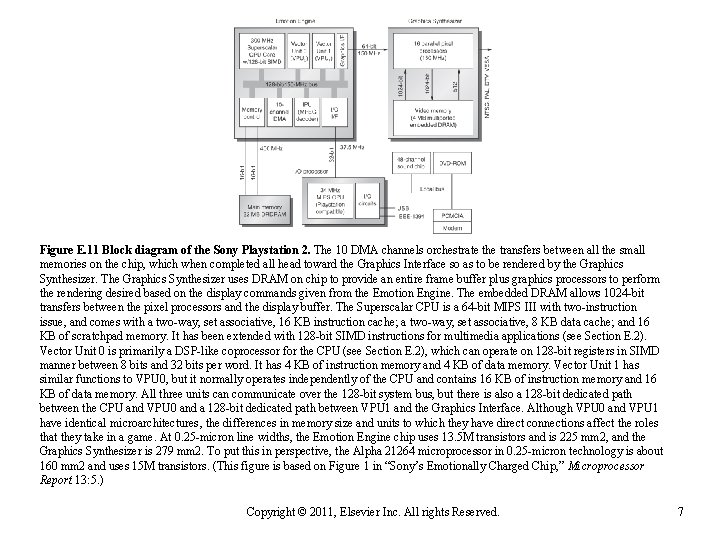
Figure E. 11 Block diagram of the Sony Playstation 2. The 10 DMA channels orchestrate the transfers between all the small memories on the chip, which when completed all head toward the Graphics Interface so as to be rendered by the Graphics Synthesizer. The Graphics Synthesizer uses DRAM on chip to provide an entire frame buffer plus graphics processors to perform the rendering desired based on the display commands given from the Emotion Engine. The embedded DRAM allows 1024 -bit transfers between the pixel processors and the display buffer. The Superscalar CPU is a 64 -bit MIPS III with two-instruction issue, and comes with a two-way, set associative, 16 KB instruction cache; a two-way, set associative, 8 KB data cache; and 16 KB of scratchpad memory. It has been extended with 128 -bit SIMD instructions for multimedia applications (see Section E. 2). Vector Unit 0 is primarily a DSP-like coprocessor for the CPU (see Section E. 2), which can operate on 128 -bit registers in SIMD manner between 8 bits and 32 bits per word. It has 4 KB of instruction memory and 4 KB of data memory. Vector Unit 1 has similar functions to VPU 0, but it normally operates independently of the CPU and contains 16 KB of instruction memory and 16 KB of data memory. All three units can communicate over the 128 -bit system bus, but there is also a 128 -bit dedicated path between the CPU and VPU 0 and a 128 -bit dedicated path between VPU 1 and the Graphics Interface. Although VPU 0 and VPU 1 have identical microarchitectures, the differences in memory size and units to which they have direct connections affect the roles that they take in a game. At 0. 25 -micron line widths, the Emotion Engine chip uses 13. 5 M transistors and is 225 mm 2, and the Graphics Synthesizer is 279 mm 2. To put this in perspective, the Alpha 21264 microprocessor in 0. 25 -micron technology is about 160 mm 2 and uses 15 M transistors. (This figure is based on Figure 1 in “Sony’s Emotionally Charged Chip, ” Microprocessor Report 13: 5. ) Copyright © 2011, Elsevier Inc. All rights Reserved. 7

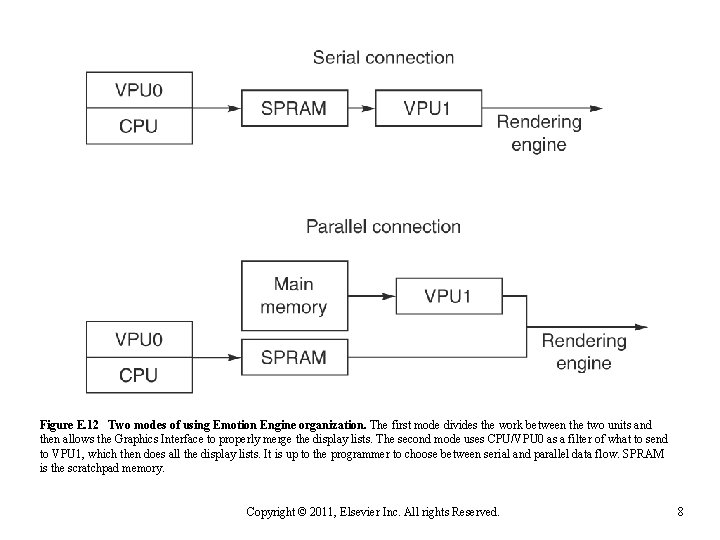
Figure E. 12 Two modes of using Emotion Engine organization. The first mode divides the work between the two units and then allows the Graphics Interface to properly merge the display lists. The second mode uses CPU/VPU 0 as a filter of what to send to VPU 1, which then does all the display lists. It is up to the programmer to choose between serial and parallel data flow. SPRAM is the scratchpad memory. Copyright © 2011, Elsevier Inc. All rights Reserved. 8

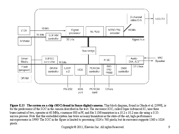
Figure E. 13 The system on a chip (SOC) found in Sanyo digital cameras. This block diagram, found in Okada et al. [1999], is for the predecessor of the SOC in the camera described in the text. The successor SOC, called Super Advanced IC, uses three buses instead of two, operates at 60 MHz, consumes 800 m. W, and fits 3. 1 M transistors in a 10. 2 x 10. 2 mm die using a 0. 35 micron process. Note that this embedded system has twice as many transistors as the state-of-the-art, high-performance microprocessor in 1990! The SOC in the figure is limited to processing 1024 x 768 pixels, but its successor supports 1360 x 1024 pixels. 9 Copyright © 2011, Elsevier Inc. All rights Reserved.

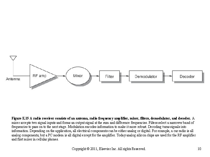
Figure E. 15 A radio receiver consists of an antenna, radio frequency amplifier, mixer, filters, demodulator, and decoder. A mixer accepts two signal inputs and forms an output signal at the sum and difference frequencies. Filters select a narrower band of frequencies to pass on to the next stage. Modulation encodes information to make it more robust. Decoding turns signals into information. Depending on the application, all electrical components can be either analog or digital. For example, a car radio is all analog components, but a PC modem is all digital except for the amplifier. Today analog silicon chips are used for the RF amplifier and first mixer in cellular phones. Copyright © 2011, Elsevier Inc. All rights Reserved. 10

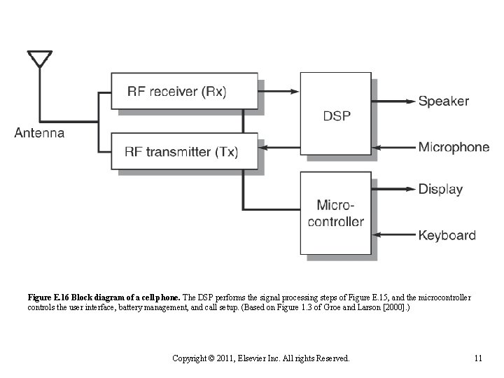
Figure E. 16 Block diagram of a cell phone. The DSP performs the signal processing steps of Figure E. 15, and the microcontroller controls the user interface, battery management, and call setup. (Based on Figure 1. 3 of Groe and Larson [2000]. ) Copyright © 2011, Elsevier Inc. All rights Reserved. 11

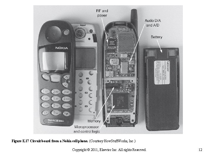
Figure E. 17 Circuit board from a Nokia cell phone. (Courtesy How. Stuff. Works, Inc. ) Copyright © 2011, Elsevier Inc. All rights Reserved. 12