Appendix D Mapping Control to Hardware Copyright 2014

- Slides: 23

Appendix D Mapping Control to Hardware Copyright © 2014 Elsevier Inc. All rights reserved.

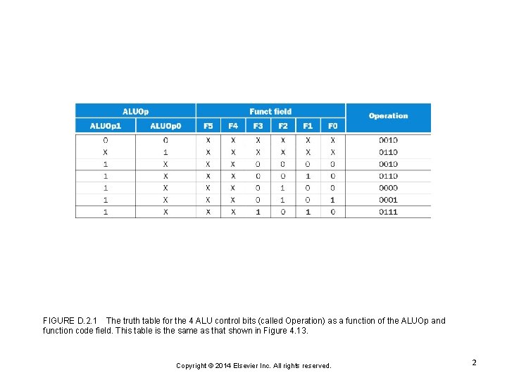
FIGURE D. 2. 1 The truth table for the 4 ALU control bits (called Operation) as a function of the ALUOp and function code field. This table is the same as that shown in Figure 4. 13. Copyright © 2014 Elsevier Inc. All rights reserved. 2

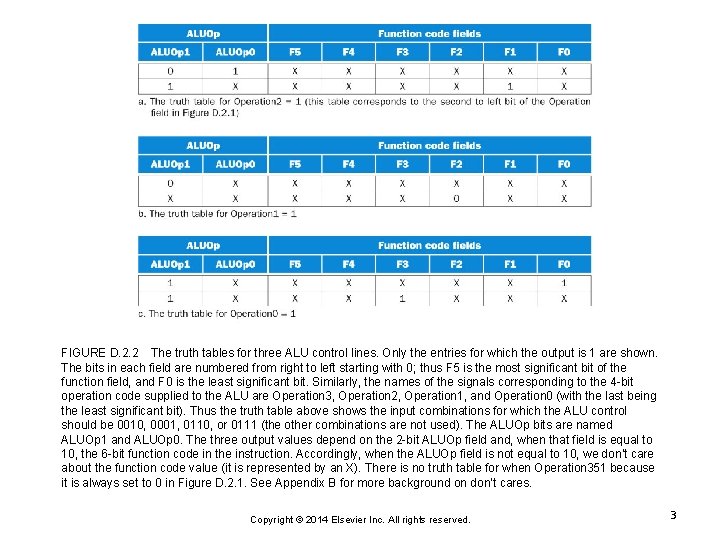
FIGURE D. 2. 2 The truth tables for three ALU control lines. Only the entries for which the output is 1 are shown. The bits in each field are numbered from right to left starting with 0; thus F 5 is the most significant bit of the function field, and F 0 is the least significant bit. Similarly, the names of the signals corresponding to the 4 -bit operation code supplied to the ALU are Operation 3, Operation 2, Operation 1, and Operation 0 (with the last being the least significant bit). Thus the truth table above shows the input combinations for which the ALU control should be 0010, 0001, 0110, or 0111 (the other combinations are not used). The ALUOp bits are named ALUOp 1 and ALUOp 0. The three output values depend on the 2 -bit ALUOp field and, when that field is equal to 10, the 6 -bit function code in the instruction. Accordingly, when the ALUOp field is not equal to 10, we don’t care about the function code value (it is represented by an X). There is no truth table for when Operation 351 because it is always set to 0 in Figure D. 2. 1. See Appendix B for more background on don’t cares. Copyright © 2014 Elsevier Inc. All rights reserved. 3

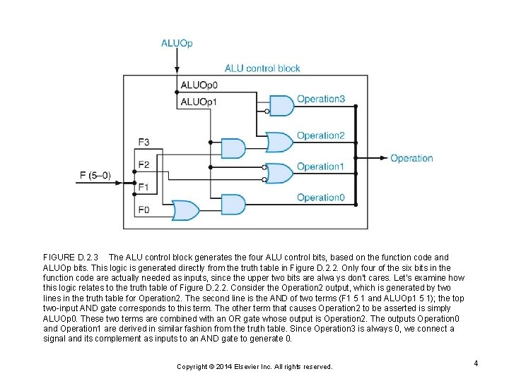
FIGURE D. 2. 3 The ALU control block generates the four ALU control bits, based on the function code and ALUOp bits. This logic is generated directly from the truth table in Figure D. 2. 2. Only four of the six bits in the function code are actually needed as inputs, since the upper two bits are alwa ys don’t cares. Let’s examine how this logic relates to the truth table of Figure D. 2. 2. Consider the Operation 2 output, which is generated by two lines in the truth table for Operation 2. The second line is the AND of two terms (F 1 5 1 and ALUOp 1 5 1); the top two-input AND gate corresponds to this term. The other term that causes Operation 2 to be asserted is simply ALUOp 0. These two terms are combined with an OR gate whose output is Operation 2. The outputs Operation 0 and Operation 1 are derived in similar fashion from the truth table. Since Operation 3 is always 0, we connect a signal and its complement as inputs to an AND gate to generate 0. Copyright © 2014 Elsevier Inc. All rights reserved. 4

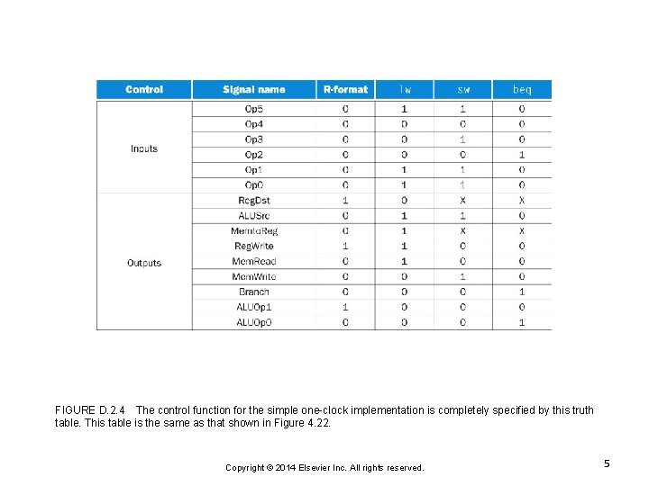
FIGURE D. 2. 4 The control function for the simple one-clock implementation is completely specified by this truth table. This table is the same as that shown in Figure 4. 22. Copyright © 2014 Elsevier Inc. All rights reserved. 5

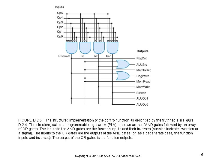
FIGURE D. 2. 5 The structured implementation of the control function as described by the truth table in Figure D. 2. 4. The structure, called a programmable logic array (PLA), uses an array of AND gates followed by an array of OR gates. The inputs to the AND gates are the function inputs and their inverses (bubbles indicate inversion of a signal). The inputs to the OR gates are the outputs of the AND gates (or, as a degenerate case, the function inputs and inverses). The output of the OR gates is the function outputs. Copyright © 2014 Elsevier Inc. All rights reserved. 6

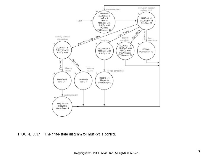
FIGURE D. 3. 1 The finite-state diagram for multicycle control. Copyright © 2014 Elsevier Inc. All rights reserved. 7

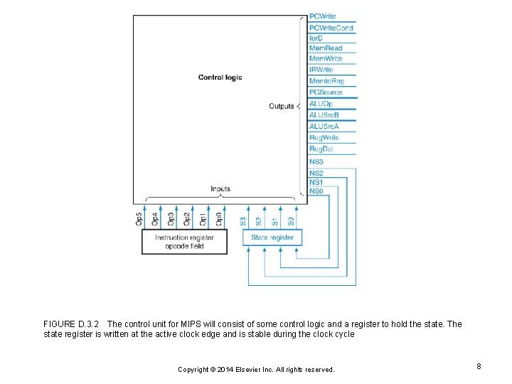
FIGURE D. 3. 2 The control unit for MIPS will consist of some control logic and a register to hold the state. The state register is written at the active clock edge and is stable during the clock cycle Copyright © 2014 Elsevier Inc. All rights reserved. 8

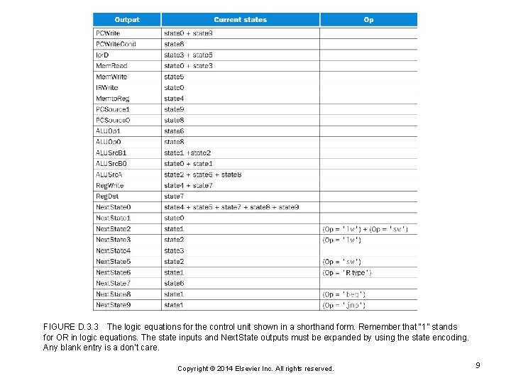
FIGURE D. 3. 3 The logic equations for the control unit shown in a shorthand form. Remember that “ 1” stands for OR in logic equations. The state inputs and Next. State outputs must be expanded by using the state encoding. Any blank entry is a don’t care. Copyright © 2014 Elsevier Inc. All rights reserved. 9

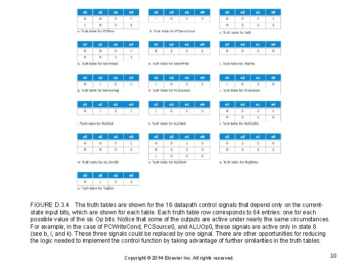
FIGURE D. 3. 4 The truth tables are shown for the 16 datapath control signals that depend only on the currentstate input bits, which are shown for each table. Each truth table row corresponds to 64 entries: one for each possible value of the six Op bits. Notice that some of the outputs are active under nearly the same circumstances. For example, in the case of PCWrite. Cond, PCSource 0, and ALUOp 0, these signals are active only in state 8 (see b, i, and k). These three signals could be replaced by one signal. There are other opportunities for reducing the logic needed to implement the control function by taking advantage of further similarities in the truth tables. Copyright © 2014 Elsevier Inc. All rights reserved. 10

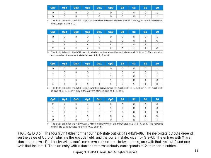
FIGURE D. 3. 5 The four truth tables for the four next-state output bits (NS[3– 0]). The next-state outputs depend on the value of Op[5 -0], which is the opcode field, and the current state, given by S[3– 0]. The entries with X are don’t-care terms. Each entry with a don’t-care term corresponds to two entries, one with that input at 0 and one with that input at 1. Thus an entry with n don’t-care terms actually corresponds to 2 n truth table entries. Copyright © 2014 Elsevier Inc. All rights reserved. 11

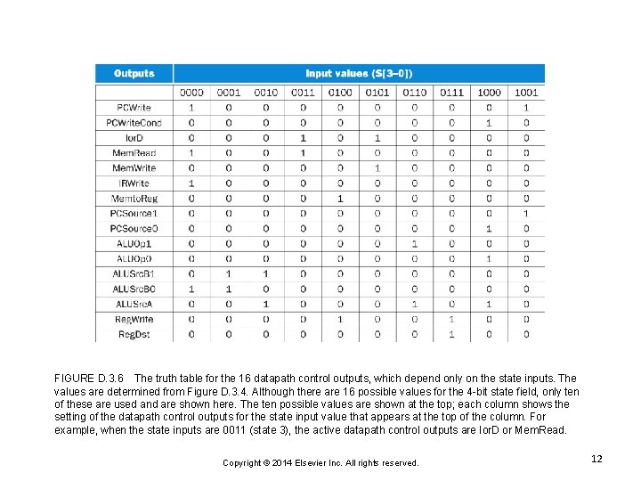
FIGURE D. 3. 6 The truth table for the 16 datapath control outputs, which depend only on the state inputs. The values are determined from Figure D. 3. 4. Although there are 16 possible values for the 4 -bit state field, only ten of these are used and are shown here. The ten possible values are shown at the top; each column shows the setting of the datapath control outputs for the state input value that appears at the top of the column. For example, when the state inputs are 0011 (state 3), the active datapath control outputs are Ior. D or Mem. Read. Copyright © 2014 Elsevier Inc. All rights reserved. 12

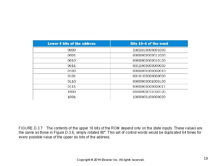
FIGURE D. 3. 7 The contents of the upper 16 bits of the ROM depend only on the state inputs. These values are the same as those in Figure D. 3. 6, simply rotated 90°. This set of control words would be duplicated 64 times for every possible value of the upper six bits of the address. Copyright © 2014 Elsevier Inc. All rights reserved. 13

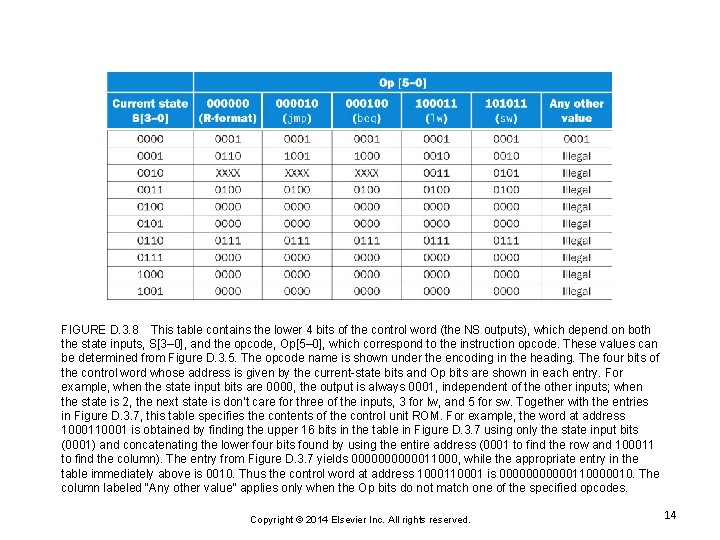
FIGURE D. 3. 8 This table contains the lower 4 bits of the control word (the NS outputs), which depend on both the state inputs, S[3– 0], and the opcode, Op[5– 0], which correspond to the instruction opcode. These values can be determined from Figure D. 3. 5. The opcode name is shown under the encoding in the heading. The four bits of the control word whose address is given by the current-state bits and Op bits are shown in each entry. For example, when the state input bits are 0000, the output is always 0001, independent of the other inputs; when the state is 2, the next state is don’t care for three of the inputs, 3 for lw, and 5 for sw. Together with the entries in Figure D. 3. 7, this table specifies the contents of the control unit ROM. For example, the word at address 10001 is obtained by finding the upper 16 bits in the table in Figure D. 3. 7 using only the state input bits (0001) and concatenating the lower four bits found by using the entire address (0001 to find the row and 100011 to find the column). The entry from Figure D. 3. 7 yields 00000011000, while the appropriate entry in the table immediately above is 0010. Thus the control word at address 10001 is 000000110000010. The column labeled “Any other value” applies only when the Op bits do not match one of the specified opcodes. Copyright © 2014 Elsevier Inc. All rights reserved. 14

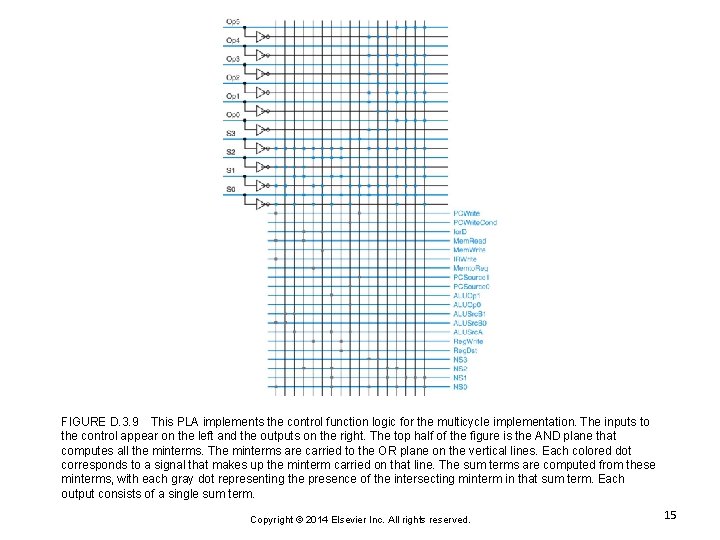
FIGURE D. 3. 9 This PLA implements the control function logic for the multicycle implementation. The inputs to the control appear on the left and the outputs on the right. The top half of the figure is the AND plane that computes all the minterms. The minterms are carried to the OR plane on the vertical lines. Each colored dot corresponds to a signal that makes up the minterm carried on that line. The sum terms are computed from these minterms, with each gray dot representing the presence of the intersecting minterm in that sum term. Each output consists of a single sum term. Copyright © 2014 Elsevier Inc. All rights reserved. 15

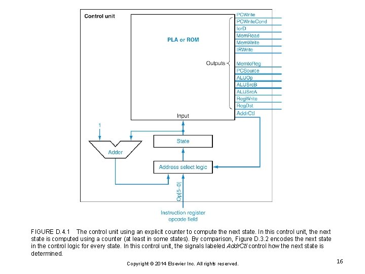
FIGURE D. 4. 1 The control unit using an explicit counter to compute the next state. In this control unit, the next state is computed using a counter (at least in some states). By comparison, Figure D. 3. 2 encodes the next state in the control logic for every state. In this control unit, the signals labeled Addr. Ctl control how the next state is determined. Copyright © 2014 Elsevier Inc. All rights reserved. 16

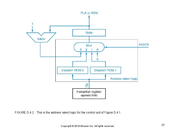
FIGURE D. 4. 2 This is the address select logic for the control unit of Figure D. 4. 1. Copyright © 2014 Elsevier Inc. All rights reserved. 17

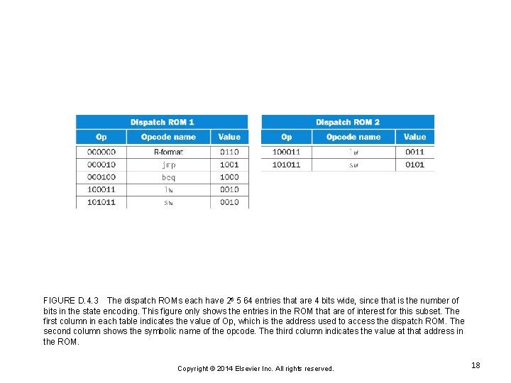
FIGURE D. 4. 3 The dispatch ROMs each have 26 5 64 entries that are 4 bits wide, since that is the number of bits in the state encoding. This figure only shows the entries in the ROM that are of interest for this subset. The first column in each table indicates the value of Op, which is the address used to access the dispatch ROM. The second column shows the symbolic name of the opcode. The third column indicates the value at that address in the ROM. Copyright © 2014 Elsevier Inc. All rights reserved. 18

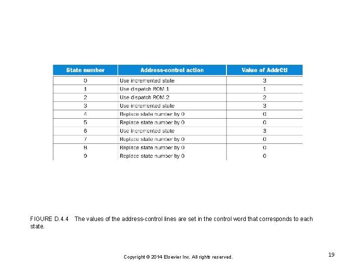
FIGURE D. 4. 4 state. The values of the address-control lines are set in the control word that corresponds to each Copyright © 2014 Elsevier Inc. All rights reserved. 19

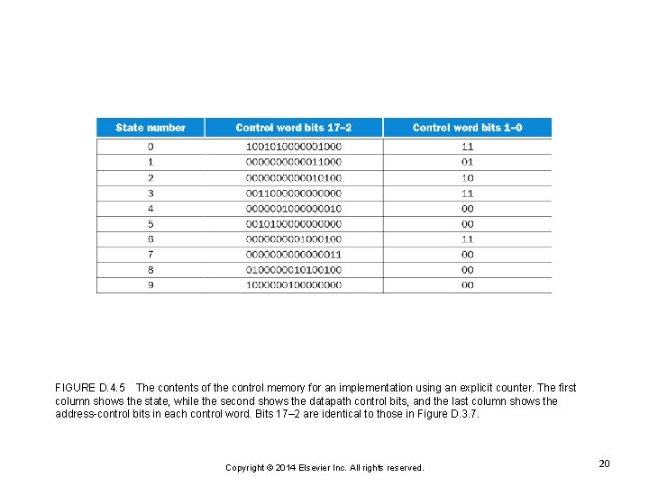
FIGURE D. 4. 5 The contents of the control memory for an implementation using an explicit counter. The first column shows the state, while the second shows the datapath control bits, and the last column shows the address-control bits in each control word. Bits 17– 2 are identical to those in Figure D. 3. 7. Copyright © 2014 Elsevier Inc. All rights reserved. 20

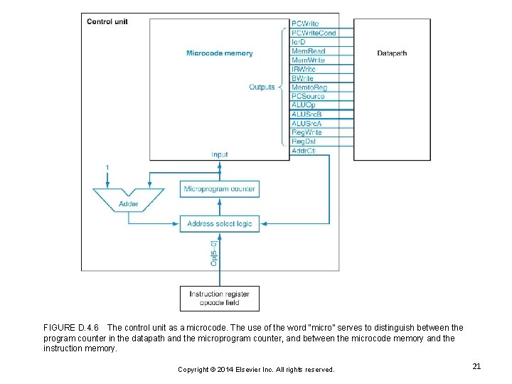
FIGURE D. 4. 6 The control unit as a microcode. The use of the word “micro” serves to distinguish between the program counter in the datapath and the microprogram counter, and between the microcode memory and the instruction memory. Copyright © 2014 Elsevier Inc. All rights reserved. 21

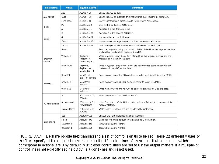
FIGURE D. 5. 1 Each microcode field translates to a set of control signals to be set. These 22 different values of the fields specify all the required combinations of the 18 control lines. Control lines that are not set, which correspond to actions, are 0 by default. Multiplexor control lines are set to 0 if the output matters. If a multiplexor control line is not explicitly set, its output is a don’t care and is not used. Copyright © 2014 Elsevier Inc. All rights reserved. 22

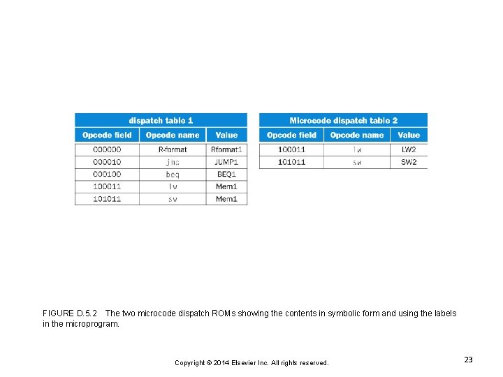
FIGURE D. 5. 2 The two microcode dispatch ROMs showing the contents in symbolic form and using the labels in the microprogram. Copyright © 2014 Elsevier Inc. All rights reserved. 23