APPENDIX A VLSI FABRICATION TECHNOLOGY Microelectronic Circuits Sixth
APPENDIX A VLSI FABRICATION TECHNOLOGY Microelectronic Circuits, Sixth Edition Sedra/Smith Copyright © 2010 by Oxford University Press, Inc.
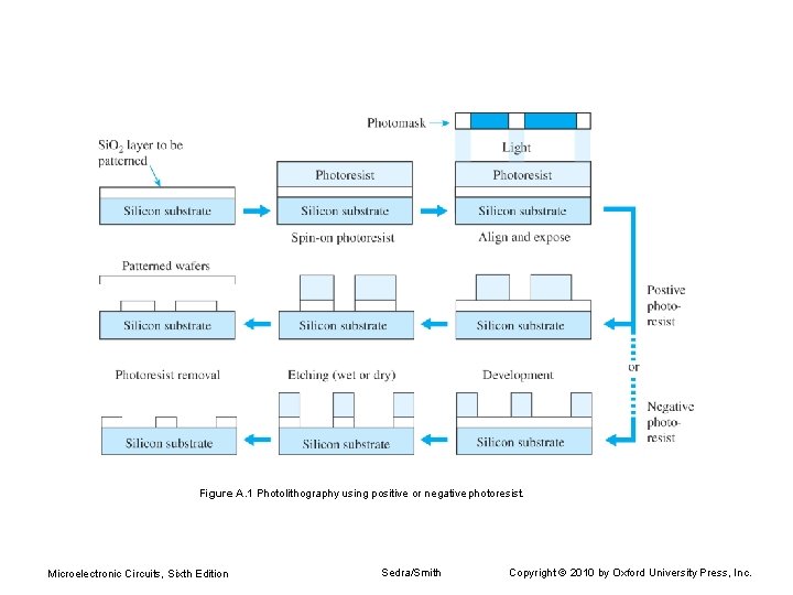
Figure A. 1 Photolithography using positive or negative photoresist. Microelectronic Circuits, Sixth Edition Sedra/Smith Copyright © 2010 by Oxford University Press, Inc.

Figure A. 2 Conceptual illustration of a step-and-repeat reduction technique to facilitate the mass production of integrated circuits. Microelectronic Circuits, Sixth Edition Sedra/Smith Copyright © 2010 by Oxford University Press, Inc.
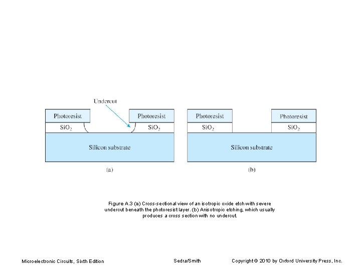
Figure A. 3 (a) Cross-sectional view of an isotropic oxide etch with severe undercut beneath the photoresist layer. (b) Anisotropic etching, which usually produces a cross section with no undercut. Microelectronic Circuits, Sixth Edition Sedra/Smith Copyright © 2010 by Oxford University Press, Inc.
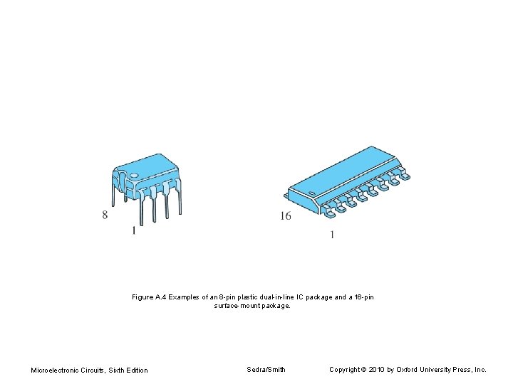
Figure A. 4 Examples of an 8 -pin plastic dual-in-line IC package and a 16 -pin surface-mount package. Microelectronic Circuits, Sixth Edition Sedra/Smith Copyright © 2010 by Oxford University Press, Inc.
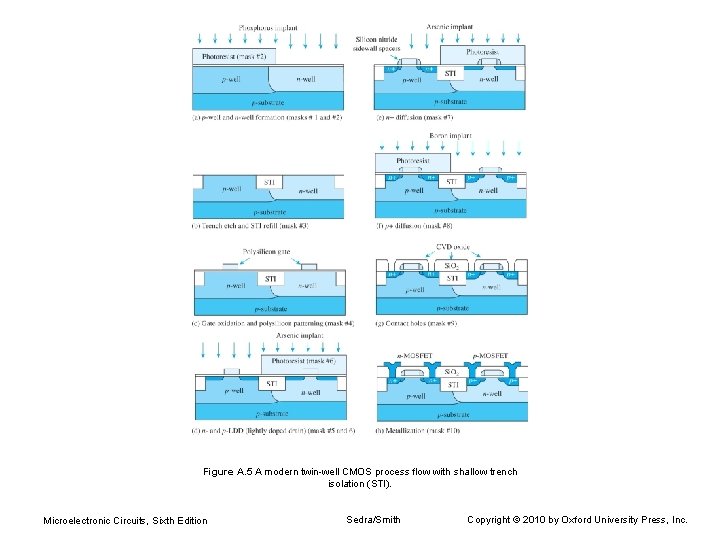
Figure A. 5 A modern twin-well CMOS process flow with shallow trench isolation (STI). Microelectronic Circuits, Sixth Edition Sedra/Smith Copyright © 2010 by Oxford University Press, Inc.
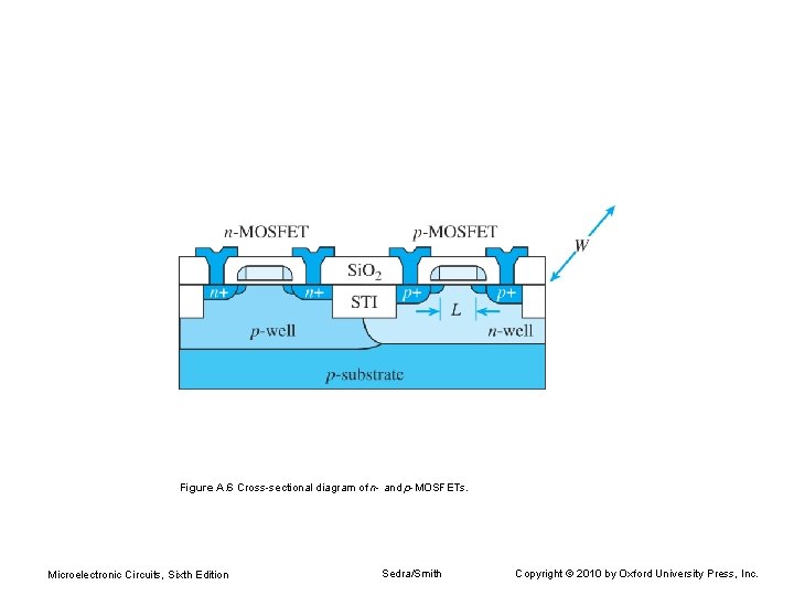
Figure A. 6 Cross-sectional diagram of n- and p-MOSFETs. Microelectronic Circuits, Sixth Edition Sedra/Smith Copyright © 2010 by Oxford University Press, Inc.
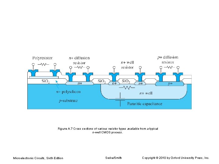
Figure A. 7 Cross sections of various resistor types available from a typical n-well CMOS process. Microelectronic Circuits, Sixth Edition Sedra/Smith Copyright © 2010 by Oxford University Press, Inc.
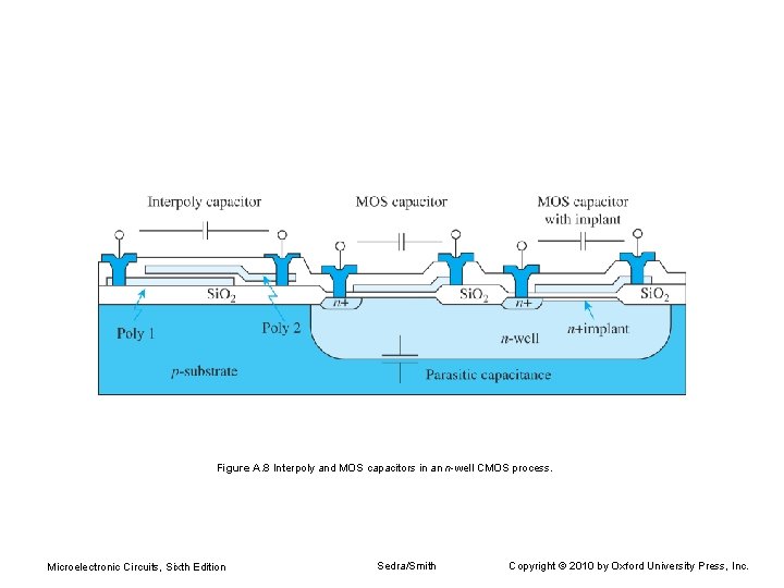
Figure A. 8 Interpoly and MOS capacitors in an n-well CMOS process. Microelectronic Circuits, Sixth Edition Sedra/Smith Copyright © 2010 by Oxford University Press, Inc.
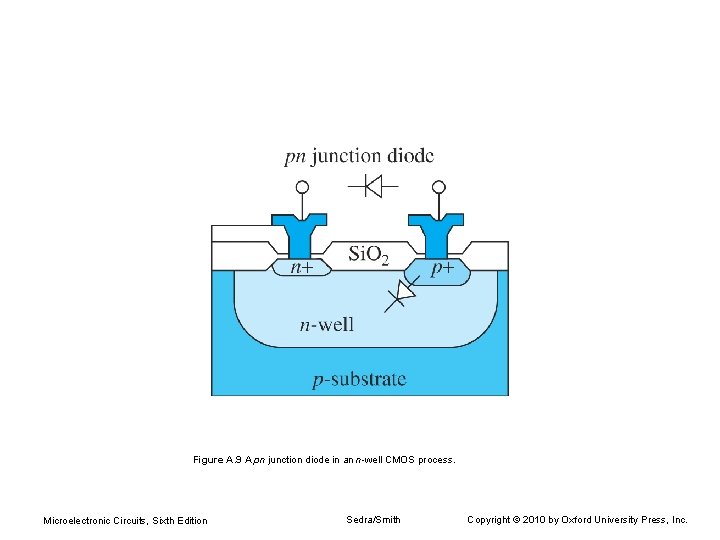
Figure A. 9 A pn junction diode in an n-well CMOS process. Microelectronic Circuits, Sixth Edition Sedra/Smith Copyright © 2010 by Oxford University Press, Inc.
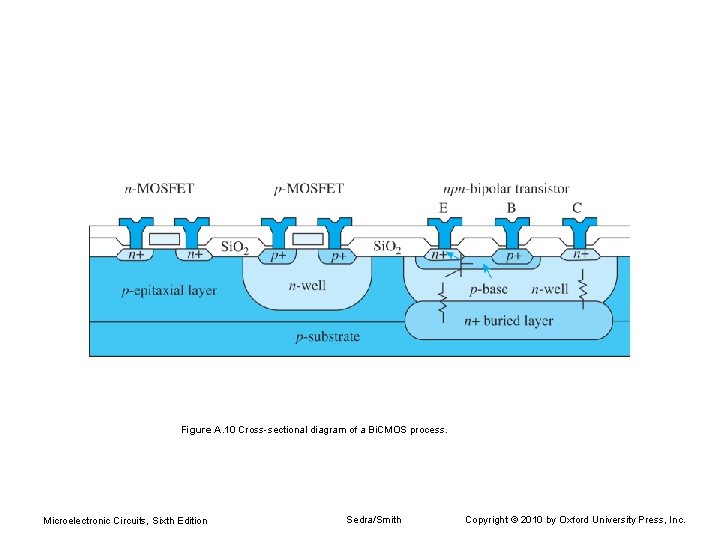
Figure A. 10 Cross-sectional diagram of a Bi. CMOS process. Microelectronic Circuits, Sixth Edition Sedra/Smith Copyright © 2010 by Oxford University Press, Inc.
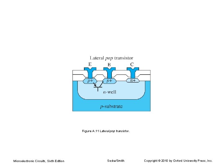
Figure A. 11 Lateral pnp transistor. Microelectronic Circuits, Sixth Edition Sedra/Smith Copyright © 2010 by Oxford University Press, Inc.
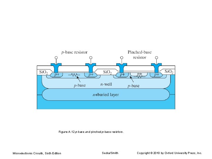
Figure A. 12 p-base and pinched p-base resistors. Microelectronic Circuits, Sixth Edition Sedra/Smith Copyright © 2010 by Oxford University Press, Inc.
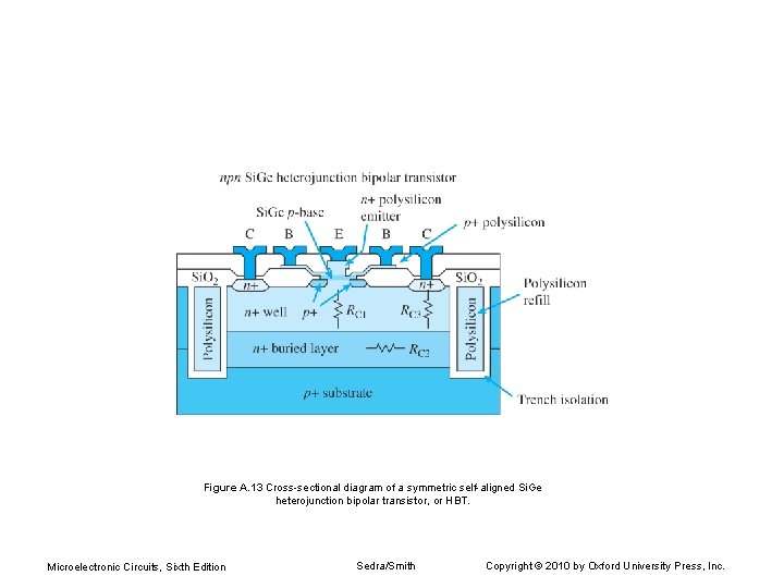
Figure A. 13 Cross-sectional diagram of a symmetric self-aligned Si. Ge heterojunction bipolar transistor, or HBT. Microelectronic Circuits, Sixth Edition Sedra/Smith Copyright © 2010 by Oxford University Press, Inc.
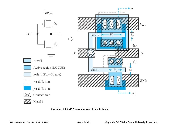
Figure A. 14 A CMOS inverter schematic and its layout. Microelectronic Circuits, Sixth Edition Sedra/Smith Copyright © 2010 by Oxford University Press, Inc.
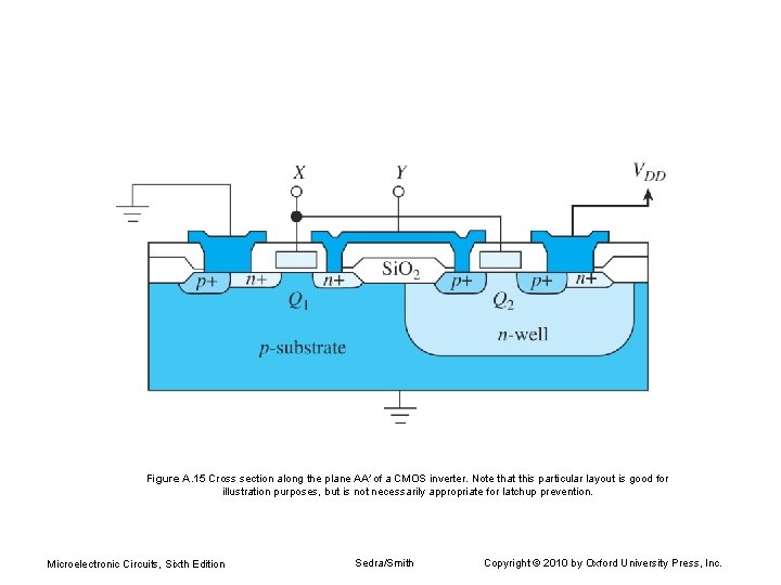
Figure A. 15 Cross section along the plane AA' of a CMOS inverter. Note that this particular layout is good for illustration purposes, but is not necessarily appropriate for latchup prevention. Microelectronic Circuits, Sixth Edition Sedra/Smith Copyright © 2010 by Oxford University Press, Inc.
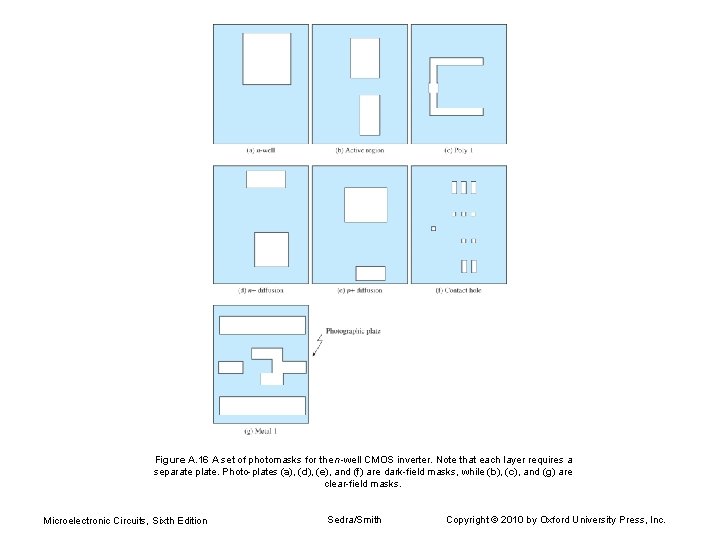
Figure A. 16 A set of photomasks for the n-well CMOS inverter. Note that each layer requires a separate plate. Photo-plates (a), (d), (e), and (f) are dark-field masks, while (b), (c), and (g) are clear-field masks. Microelectronic Circuits, Sixth Edition Sedra/Smith Copyright © 2010 by Oxford University Press, Inc.
- Slides: 17