Anjuman College of Engg Technology Sadar Nagpur Department






- Slides: 15

Anjuman College of Engg. & Technology Sadar, Nagpur Department of Electronics & Telecommunication Engineering Fifth Semester Microprocessor and Microcontrollers Topic: IC 8288 External Bus Controller Mohammad Nasiruddin Associate Professor and HOD mn 151819@gmail. com

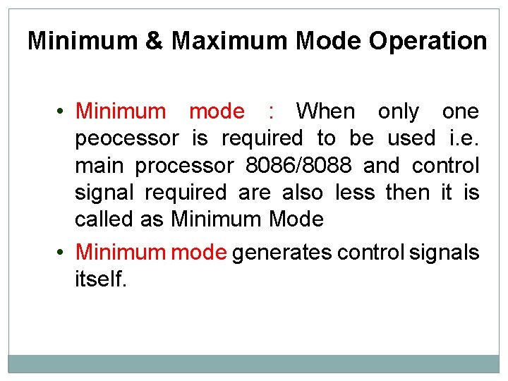
Minimum & Maximum Mode Operation • Minimum mode : When only one peocessor is required to be used i. e. main processor 8086/8088 and control signal required are also less then it is called as Minimum Mode • Minimum mode generates control signals itself.

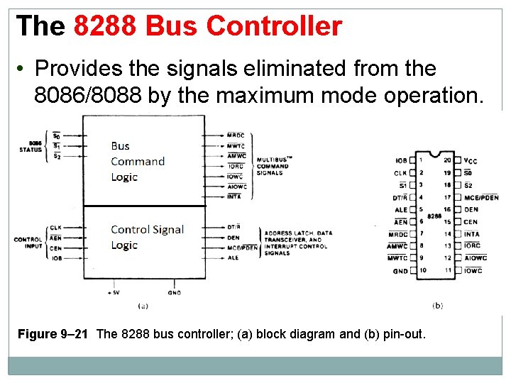
• There are not enough pins on the 8086 for bus control during maximum mode, so it requires addition of the IC 8288 external bus controller. • Maximum mode is used only when the system contains external coprocessors such as 8087 NDP and 8089 IOP.

The 8288 Bus Controller • Provides the signals eliminated from the 8086/8088 by the maximum mode operation. Figure 9– 21 The 8288 bus controller; (a) block diagram and (b) pin-out.

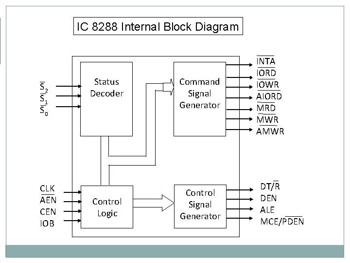
IC 8288 Internal Block Diagram S 2 S 1 S 0 CLK AEN CEN IOB Status Decoder Control Logic Command Signal Generator Control Signal Generator INTA IORD IOWR AIORD MWR AMWR DT/R DEN ALE MCE/PDEN

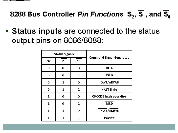
8288 Bus Controller Pin Functions S 2, S 1, and S 0 • Status inputs are connected to the status output pins on 8086/8088: Status Signals Command Signal Generated S 2 S 1 S 0 0 INTA 0 0 1 IORD 0 1 0 IOWR/AIOWR 0 1 1 HALT State 1 0 0 OPCODE fetch operation 1 0 1 MRD 1 1 0 MWR/AMWR 1 1 1 Passive

CLK • The clock input provides internal timing. The CLK output pin of the 8284 signal generator is connected to CLK pin of IC 8288. ALE • The address latch enable output is used to demultiplex the address/data bus and address/status by using Latch IC 8288.

DEN • The data bus enable pin is used to enable the transreceiver IC 8286 which controls the bidirectional data bus in the system. DT/R • Data transmit/receive signal output to control direction of the bidirectional data bus buffers available in IC 8286.

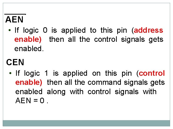
AEN • If logic 0 is applied to this pin (address enable) then all the control signals gets enabled. CEN • If logic 1 is applied on this pin (control enable) then all the command signals gets enabled along with control signals with AEN = 0.

IOB • The I/O bus mode input selects either I/O bus mode or system bus mode operation. If IOB = 1 then I/O bus mode is selected and PDEN = 0 But if IOB = 0 then system bus mode is selected and MCE = 1

AIOWR • Advanced I/O write is a command output to an advanced I/O write control signal. IORD • The I/O read command output provides I/O with its read control signal. IOWR • The I/O write command output provides I/O with its write control signal.

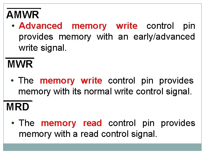
AMWR • Advanced memory write control pin provides memory with an early/advanced write signal. MWR • The memory write control pin provides memory with its normal write control signal. MRD • The memory read control pin provides memory with a read control signal.

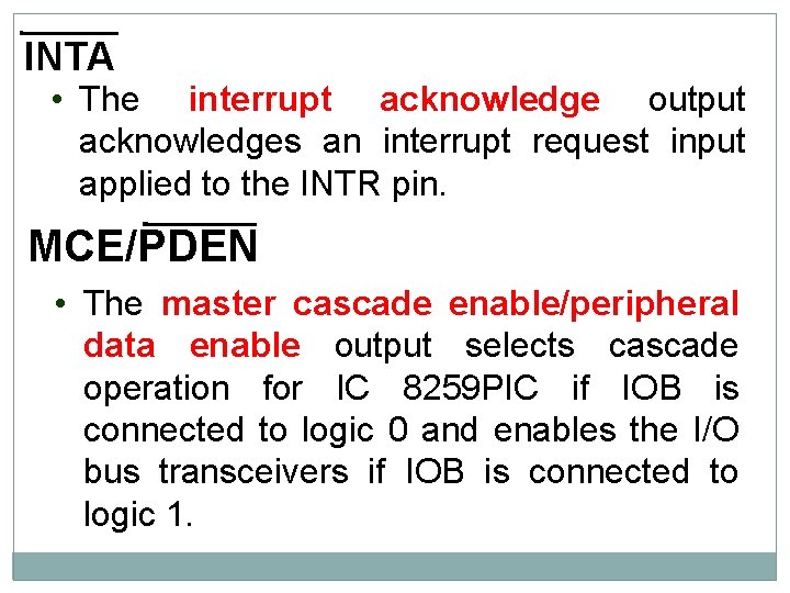
INTA • The interrupt acknowledge output acknowledges an interrupt request input applied to the INTR pin. MCE/PDEN • The master cascade enable/peripheral data enable output selects cascade operation for IC 8259 PIC if IOB is connected to logic 0 and enables the I/O bus transceivers if IOB is connected to logic 1.

SUMMARY • Minimum mode operation is similar to that of the Intel 8085 A microprocessor, whereas maximum mode operation is new and specifically designed for the operation of the 8087 arithmetic coprocessor. • The 8288 bus controller must be used in the maximum mode to provide the control bus signals to the memory and I/O.

• This is because the maximum mode operation of the 8086/8088 removes some of the system's control signal lines in favor of control signals for the coprocessors. • The 8288 bus controller reconstructs these removed control signals.
 The silenced by nadia anjuman
 Engg2780
 Civil house drawing
 Engg 1100
 Engg 1100
 Manajemen risiko
 Struktur organisasi manajemen risiko perusahaan
 Keluarga sadar gizi
 Contoh kasus asas tiada pidana tanpa kesalahan
 Kesadaran berbangsa dan bernegara bangkit
 Usaha sadar adalah
 Visvesvaraya technological university nagpur
 Public health institute nagpur
 Mount litera zee school learning resources pdf
 Ddu gky nagpur
 Classification of roads by nagpur road plan

