Analytical Transmissions Electron Microscopy TEM Part I The
- Slides: 30

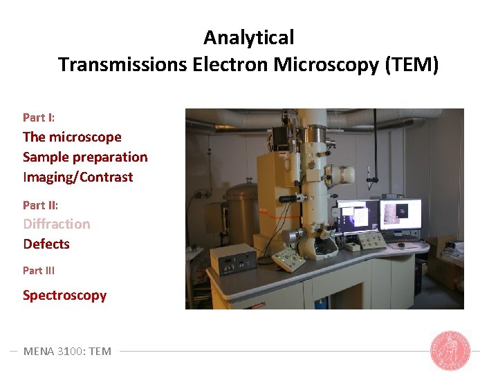
Analytical Transmissions Electron Microscopy (TEM) Part I: The microscope Sample preparation Imaging/Contrast Part II: Diffraction Defects Part III Spectroscopy MENA 3100: TEM

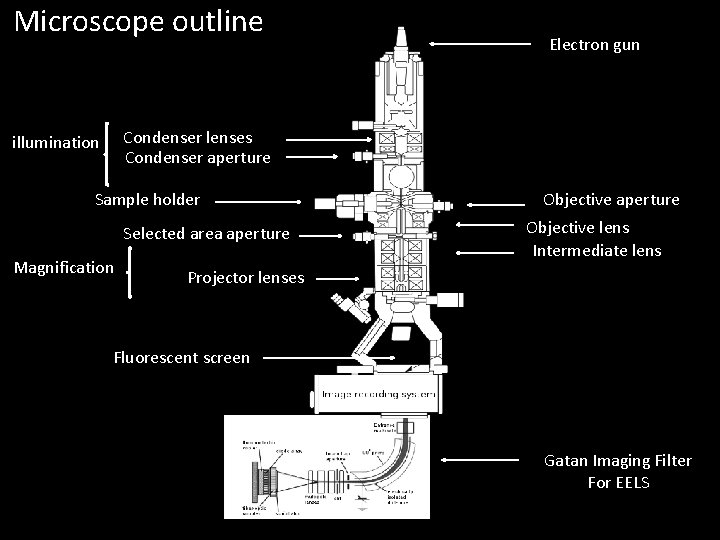
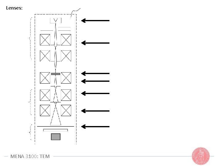
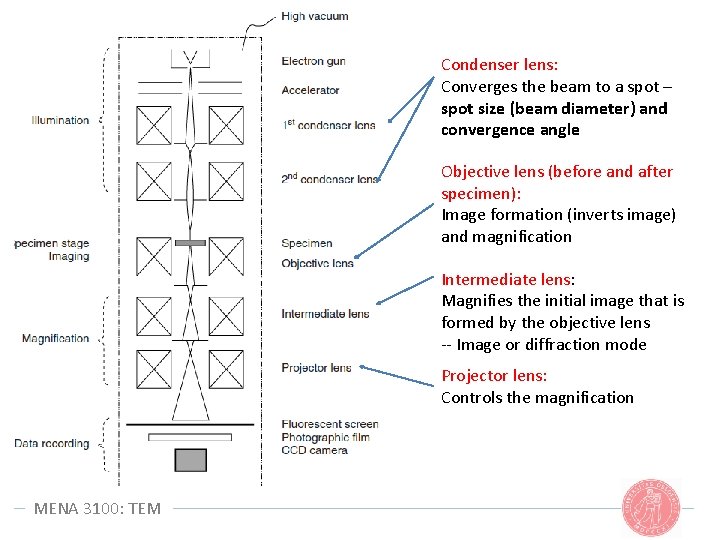
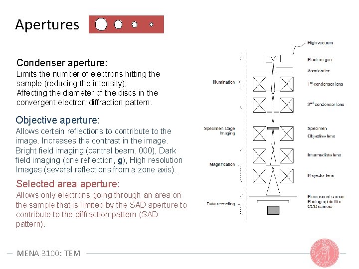
Microscope outline Electron gun Condenser lenses Condenser aperture illumination Sample holder Selected area aperture Magnification Objective aperture Objective lens Intermediate lens Projector lenses Fluorescent screen Gatan Imaging Filter For EELS

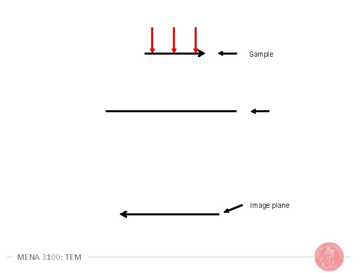
Sample Objective lens Image plane MENA 3100: TEM

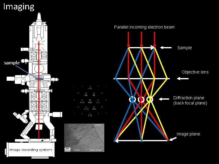
Imaging Parallel incoming electron beam Sample sample Objective lens Diffraction plane (back focal plane) Image plane

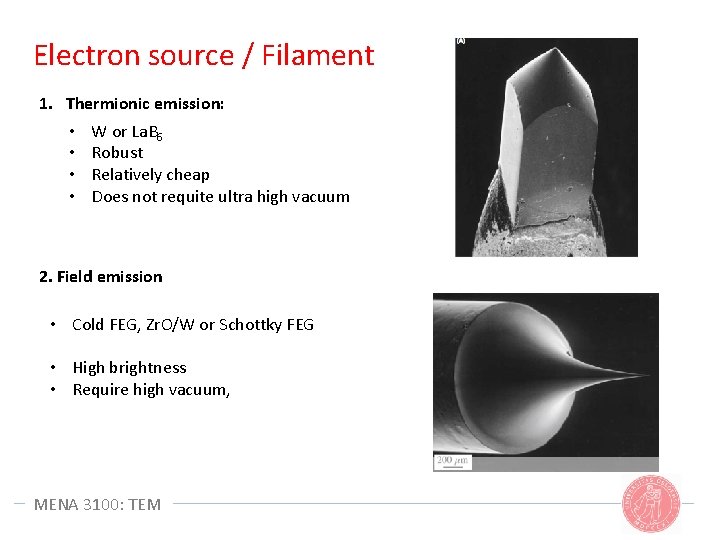
Electron source / Filament 1. Thermionic emission: • • W or La. B 6 Robust Relatively cheap Does not requite ultra high vacuum 2. Field emission • Cold FEG, Zr. O/W or Schottky FEG • High brightness • Require high vacuum, MENA 3100: TEM

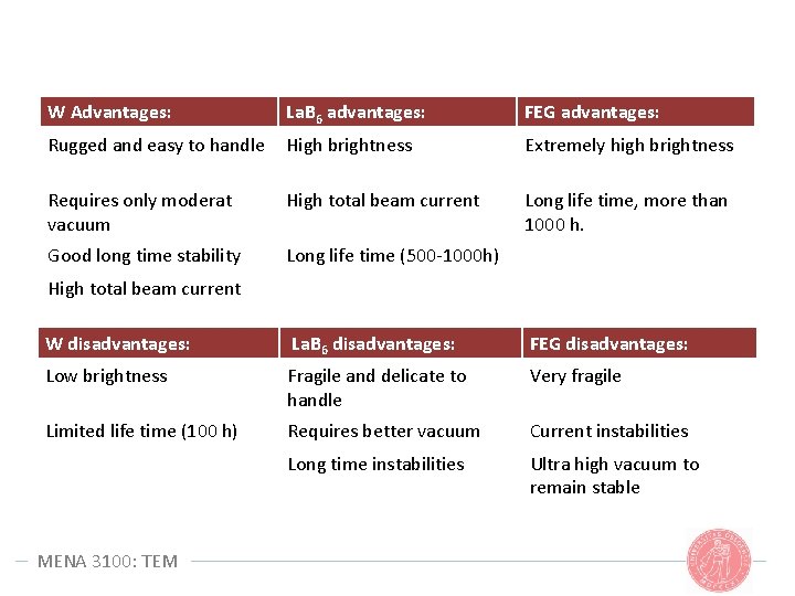
W Advantages: La. B 6 advantages: FEG advantages: Rugged and easy to handle High brightness Extremely high brightness Requires only moderat vacuum High total beam current Long life time, more than 1000 h. Good long time stability Long life time (500 -1000 h) High total beam current W disadvantages: La. B 6 disadvantages: FEG disadvantages: Low brightness Fragile and delicate to handle Very fragile Limited life time (100 h) Requires better vacuum Current instabilities Long time instabilities Ultra high vacuum to remain stable MENA 3100: TEM

Lenses: MENA 3100: TEM

Condenser lens: Converges the beam to a spot – spot size (beam diameter) and convergence angle Objective lens (before and after specimen): Image formation (inverts image) and magnification Intermediate lens: Magnifies the initial image that is formed by the objective lens -- Image or diffraction mode Projector lens: Controls the magnification MENA 3100: TEM

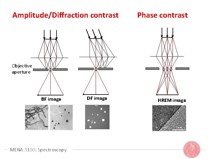
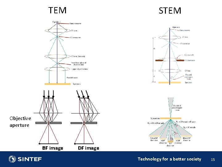
Apertures Condenser aperture: Limits the number of electrons hitting the sample (reducing the intensity), Affecting the diameter of the discs in the convergent electron diffraction pattern. Objective aperture: Allows certain reflections to contribute to the image. Increases the contrast in the image. Bright field imaging (central beam, 000), Dark field imaging (one reflection, g), High resolution Images (several reflections from a zone axis). Selected area aperture: Allows only electrons going through an area on the sample that is limited by the SAD aperture to contribute to the diffraction pattern (SAD pattern). MENA 3100: TEM

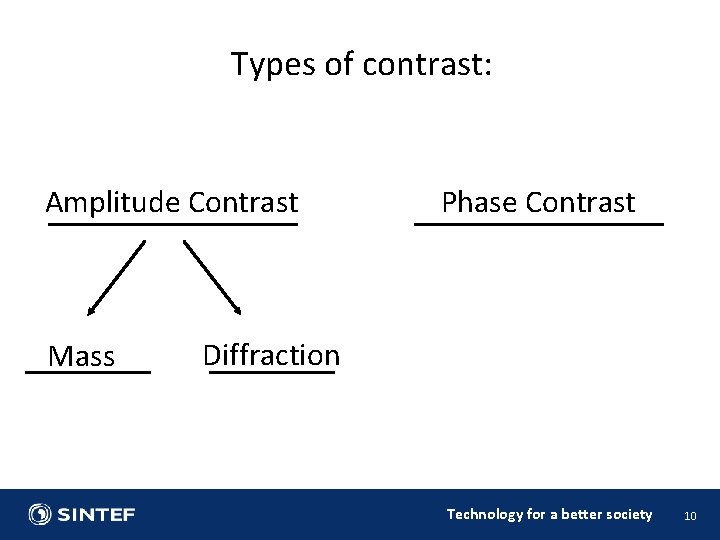
Types of contrast: Amplitude Contrast Mass Phase Contrast Diffraction Technology for a better society 10

Amplitude/Diffraction contrast Phase contrast Objective aperture BF image MENA 3100: Spectroscopy DF image HREM image

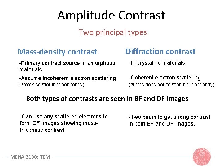
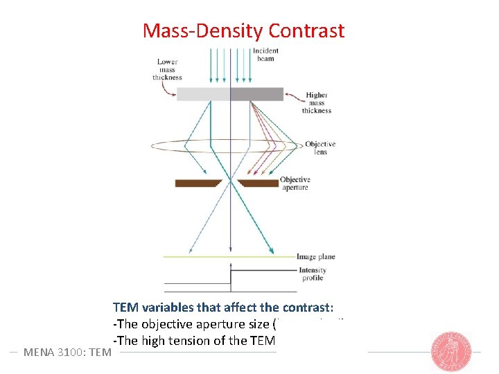
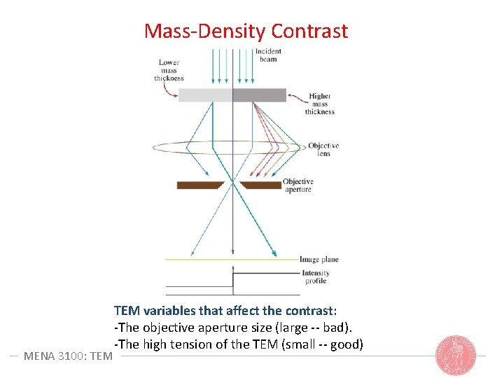
Amplitude Contrast Two principal types Mass-density contrast Diffraction contrast -Primary contrast source in amorphous materials -In crystaline materials -Assume incoherent electron scattering -Coherent electron scattering (atoms scatter independently) (atoms does not scatter independently) Both types of contrasts are seen in BF and DF images -Can use any scattered electrons to form DF images showing massthickness contrast MENA 3100: TEM -Two beam to get strong contrast in both BF and DF images.

Mass-Density Contrast MENA 3100: TEM variables that affect the contrast: -The objective aperture size (large -- bad). -The high tension of the TEM (small -- good)

Mass-Density Contrast MENA 3100: TEM variables that affect the contrast: -The objective aperture size (large -- bad). -The high tension of the TEM (small -- good)

TEM STEM Objective aperture BF image DF image Technology for a better society 15

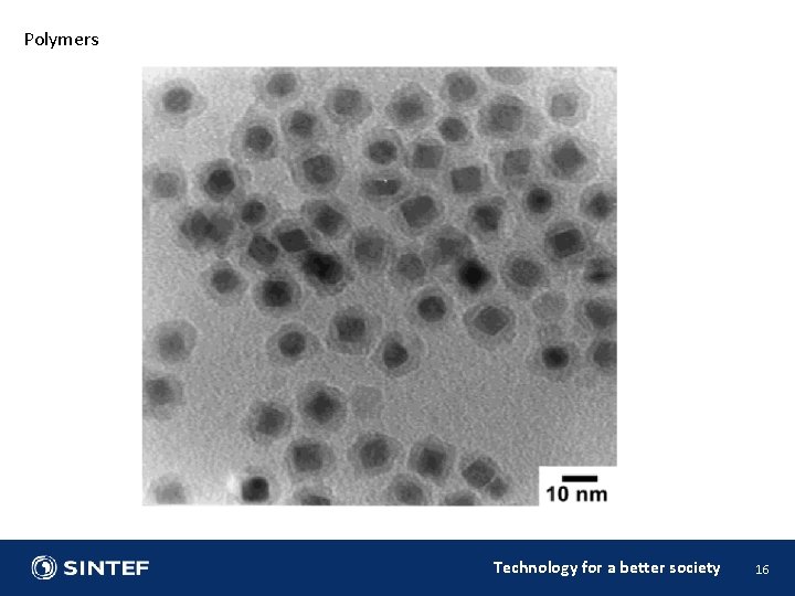
Polymers Technology for a better society 16

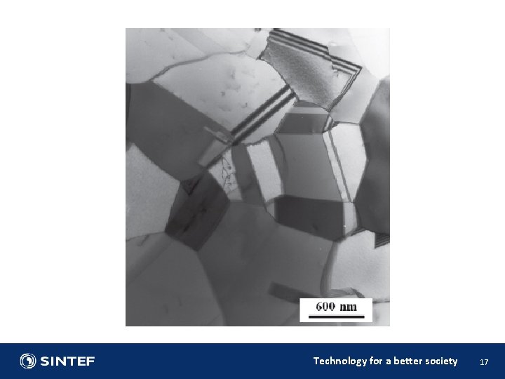
Technology for a better society 17

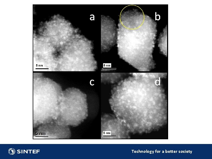
Technology for a better society

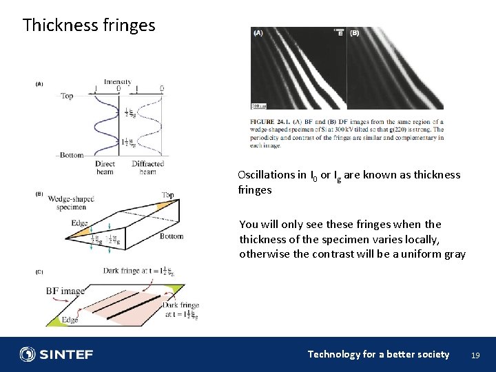
Thickness fringes Oscillations in I 0 or Ig are known as thickness fringes You will only see these fringes when the thickness of the specimen varies locally, otherwise the contrast will be a uniform gray Technology for a better society 19

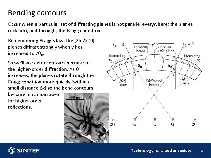
Bending contours Occur when a particular set of diffracting planes is not parallel everywhere; the planes rock into, and through, the Bragg condition. Remembering Bragg’s law, the (2 h 2 k 2 l) planes diffract strongly when y has increased to 2θB. So we’ll see extra contours because of the higher-order diffraction. As θ increases, the planes rotate through the Bragg condition more quickly (within a small distance Δx) so the bend contours become much narrower for higher order reflections. Technology for a better society 20

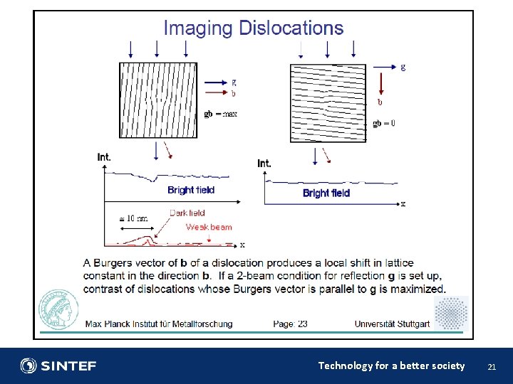
Technology for a better society 21

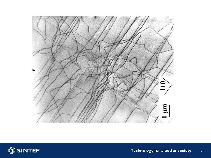
Technology for a better society 22

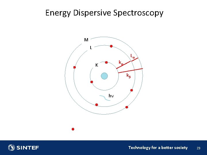
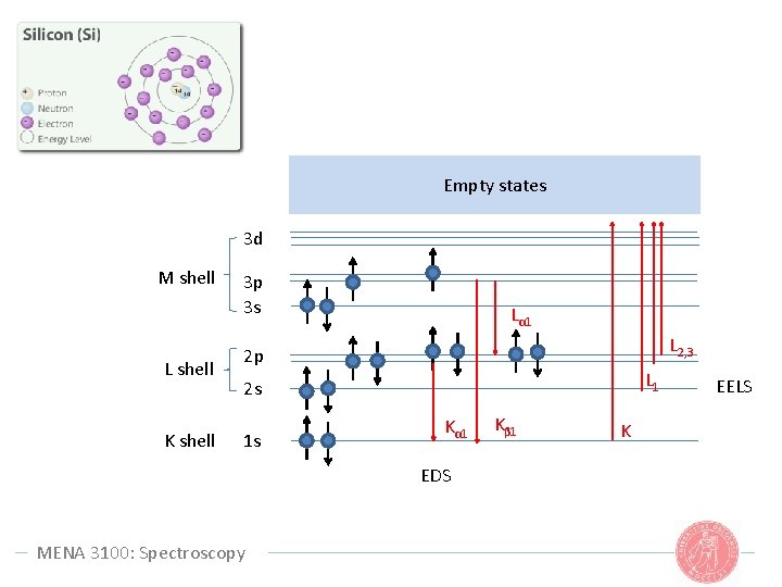
Energy Dispersive Spectroscopy M L kα K Lα kβ hν Technology for a better society 23

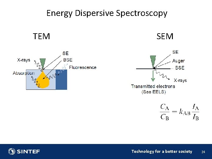
Energy Dispersive Spectroscopy TEM SEM Technology for a better society 24

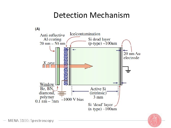
Detection Mechanism MENA 3100: Spectroscopy

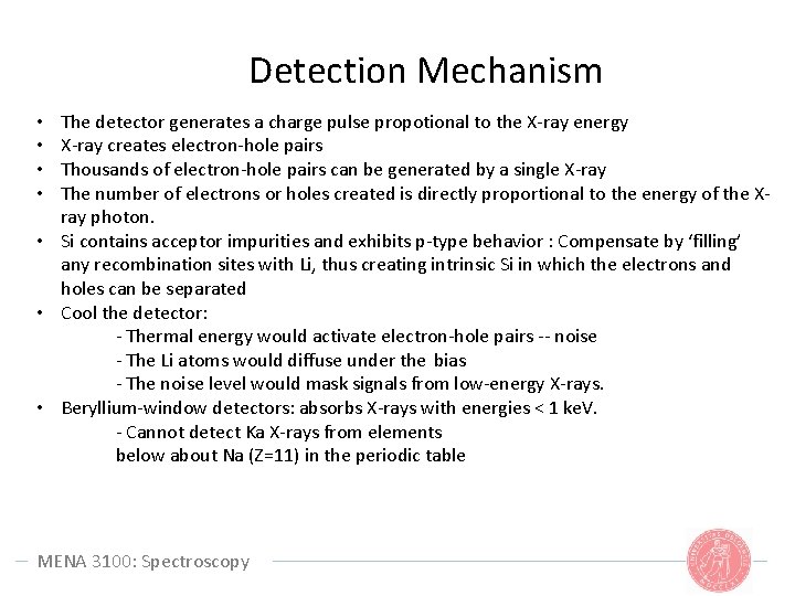
Detection Mechanism The detector generates a charge pulse propotional to the X-ray energy X-ray creates electron-hole pairs Thousands of electron-hole pairs can be generated by a single X-ray The number of electrons or holes created is directly proportional to the energy of the Xray photon. • Si contains acceptor impurities and exhibits p-type behavior : Compensate by ‘filling’ any recombination sites with Li, thus creating intrinsic Si in which the electrons and holes can be separated • Cool the detector: - Thermal energy would activate electron-hole pairs -- noise - The Li atoms would diffuse under the bias - The noise level would mask signals from low-energy X-rays. • Beryllium-window detectors: absorbs X-rays with energies < 1 ke. V. - Cannot detect Ka X-rays from elements below about Na (Z=11) in the periodic table • • MENA 3100: Spectroscopy

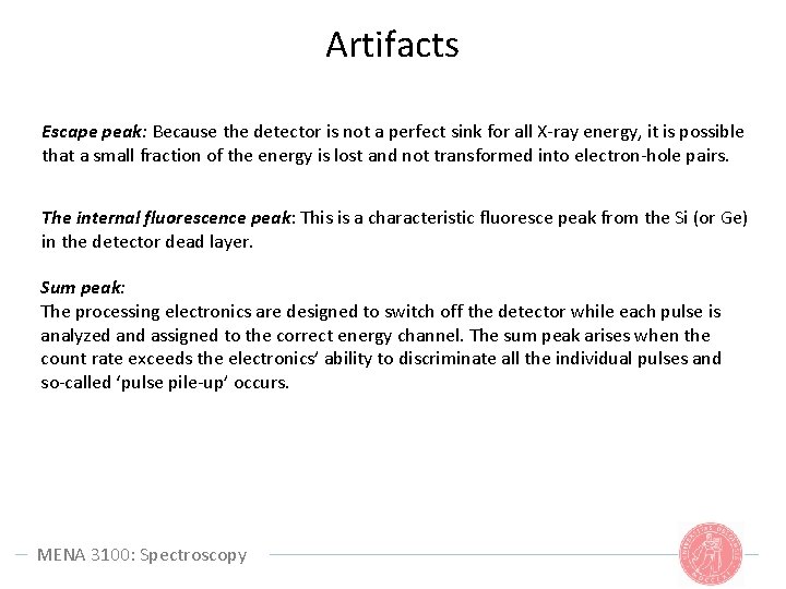
Artifacts Escape peak: Because the detector is not a perfect sink for all X-ray energy, it is possible that a small fraction of the energy is lost and not transformed into electron-hole pairs. The internal fluorescence peak: This is a characteristic fluoresce peak from the Si (or Ge) in the detector dead layer. Sum peak: The processing electronics are designed to switch off the detector while each pulse is analyzed and assigned to the correct energy channel. The sum peak arises when the count rate exceeds the electronics’ ability to discriminate all the individual pulses and so-called ‘pulse pile-up’ occurs. MENA 3100: Spectroscopy

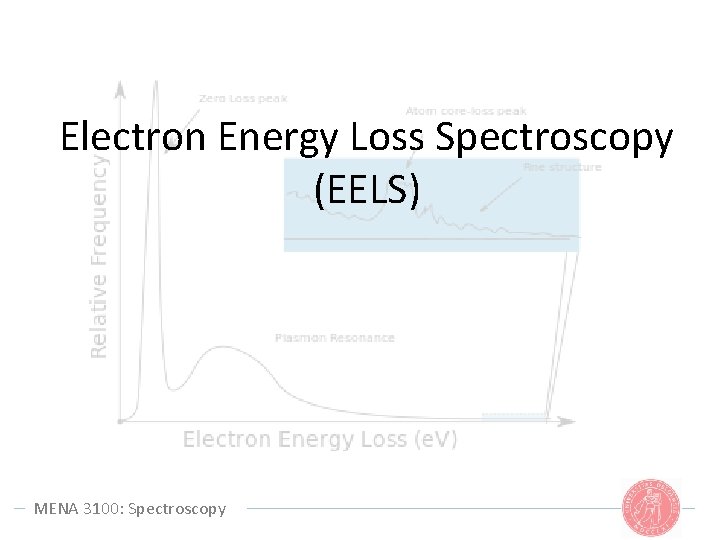
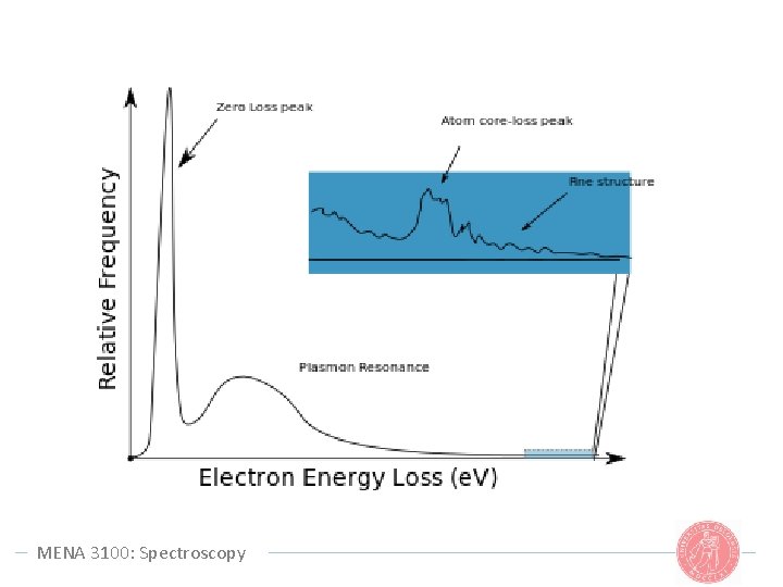
Electron Energy Loss Spectroscopy (EELS) MENA 3100: Spectroscopy

Empty states 3 d M shell L shell K shell 3 p 3 s Lα 1 L 2, 3 2 p L 1 2 s 1 s Kα 1 EDS MENA 3100: Spectroscopy Kβ 1 K EELS

MENA 3100: Spectroscopy