Analytical Transmissions Electron Microscopy TEM Part I The
- Slides: 54

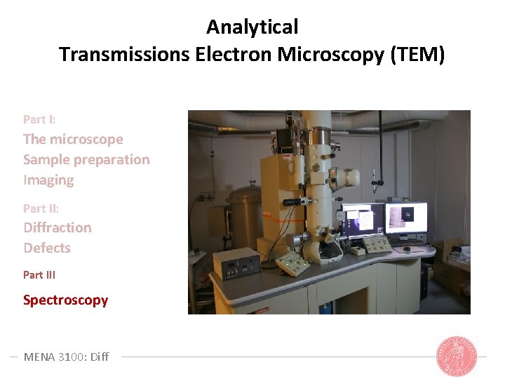
Analytical Transmissions Electron Microscopy (TEM) Part I: The microscope Sample preparation Imaging Part II: Diffraction Defects Part III Spectroscopy MENA 3100: Diff

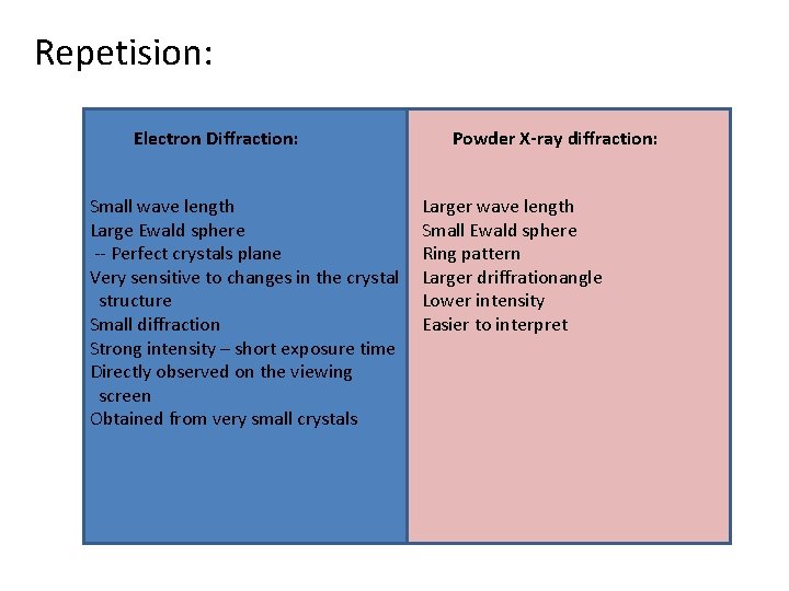
Repetision: Electron Diffraction: Small wave length Large Ewald sphere -- Perfect crystals plane Very sensitive to changes in the crystal structure Small diffraction Strong intensity – short exposure time Directly observed on the viewing screen Obtained from very small crystals Powder X-ray diffraction: Larger wave length Small Ewald sphere Ring pattern Larger driffrationangle Lower intensity Easier to interpret

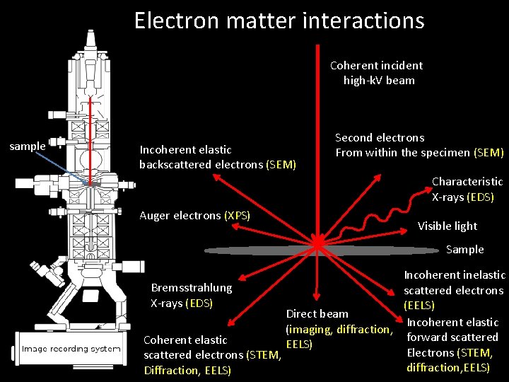
Electron matter interactions Coherent incident high-k. V beam sample Incoherent elastic backscattered electrons (SEM) Second electrons From within the specimen (SEM) Characteristic X-rays (EDS) Auger electrons (XPS) Visible light Sample Incoherent inelastic Bremsstrahlung scattered electrons X-rays (EDS) (EELS) Direct beam Incoherent elastic (imaging, diffraction, forward scattered Coherent elastic EELS) Electrons (STEM, scattered electrons (STEM, diffraction, EELS) Diffraction, EELS)

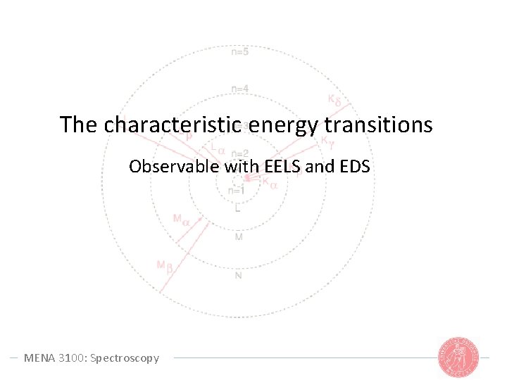
The characteristic energy transitions Observable with EELS and EDS MENA 3100: Spectroscopy

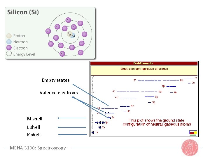
Empty states Valence electrons M shell L shell K shell MENA 3100: Spectroscopy

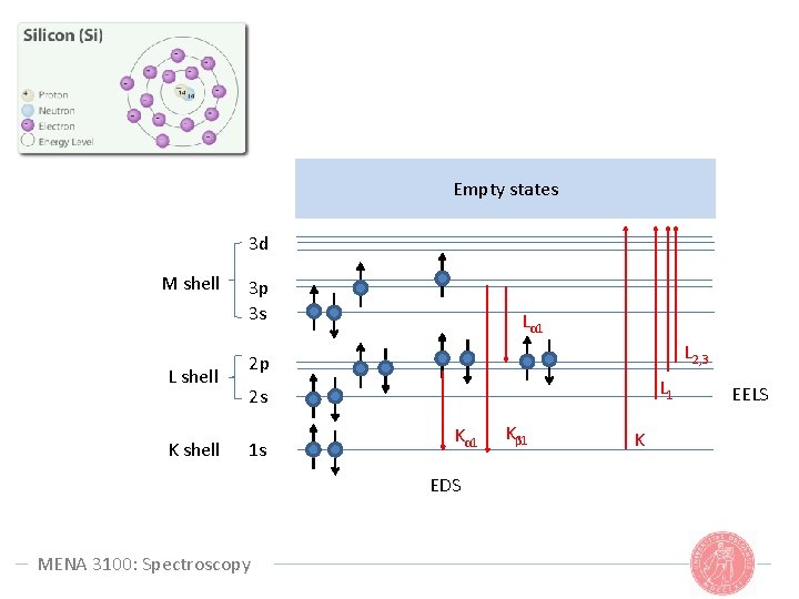
Empty states 3 d M shell L shell K shell 3 p 3 s Lα 1 L 2, 3 2 p L 1 2 s 1 s Kα 1 EDS MENA 3100: Spectroscopy Kβ 1 K EELS

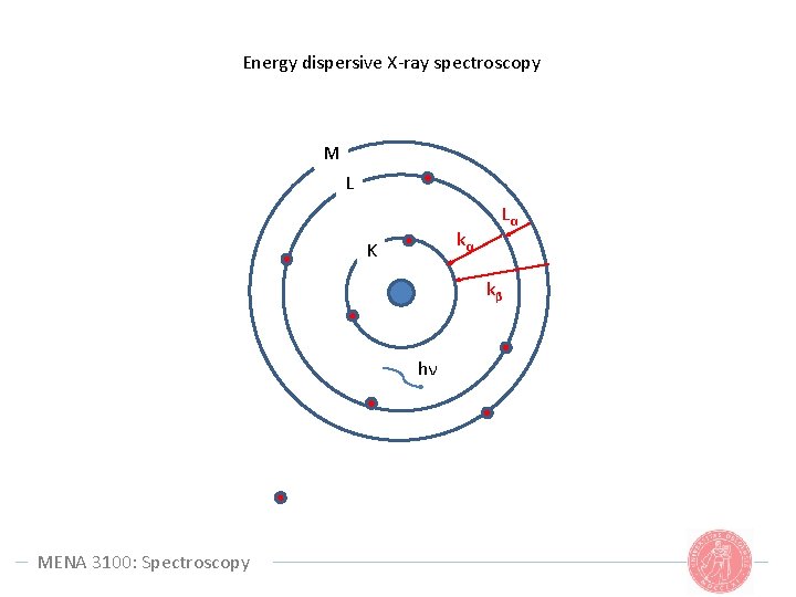
Energy dispersive X-ray spectroscopy M L kα K Lα kβ hν MENA 3100: Spectroscopy

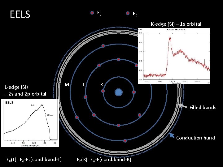
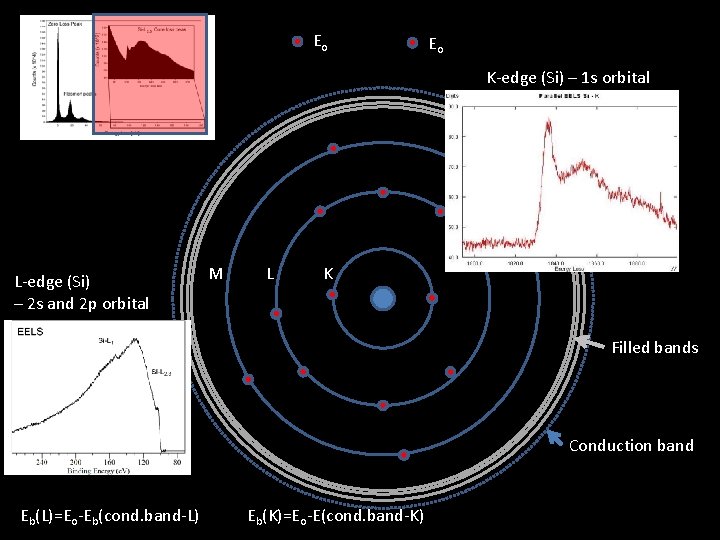
EELS L-edge (Si) – 2 s and 2 p orbital Eo Eo K-edge (Si) – 1 s orbital M L K Filled bands Conduction band Eb(L)=Eo-Eb(cond. band-L) Eb(K)=Eo-E(cond. band-K)

Energy Dispersive X-ray Spectroscopy (EDS) MENA 3100: Spectroscopy

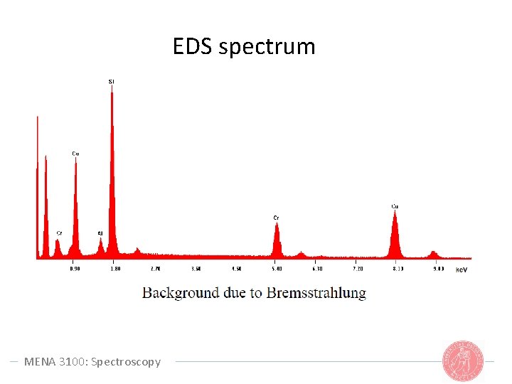
EDS spectrum MENA 3100: Spectroscopy

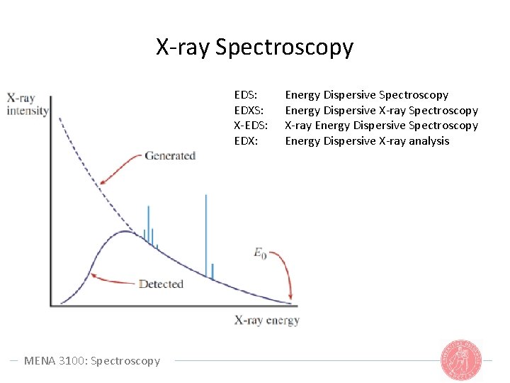
X-ray Spectroscopy EDS: EDXS: X-EDS: EDX: MENA 3100: Spectroscopy Energy Dispersive X-ray Spectroscopy X-ray Energy Dispersive Spectroscopy Energy Dispersive X-ray analysis

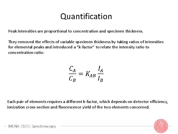
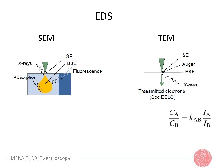
Quantification Peak intensities are proportional to concentration and specimen thickness. They removed the effects of variable specimen thickness by taking ratios of intensities for elemental peaks and introduced a “k-factor” to relate the intensity ratio to concentration ratio: Each pair of elements requires a different k-factor, which depends on detector efficiency, ionization cross-section and fluorescence yield of the two elements concerned. MENA 3100: Spectroscopy

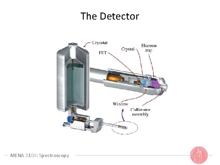
The Detector MENA 3100: Spectroscopy

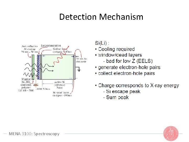
Detection Mechanism MENA 3100: Spectroscopy

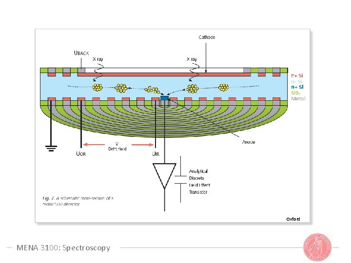
Oxford MENA 3100: Spectroscopy

EDS SEM MENA 3100: Spectroscopy TEM

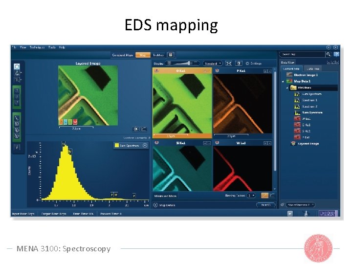
EDS mapping MENA 3100: Spectroscopy

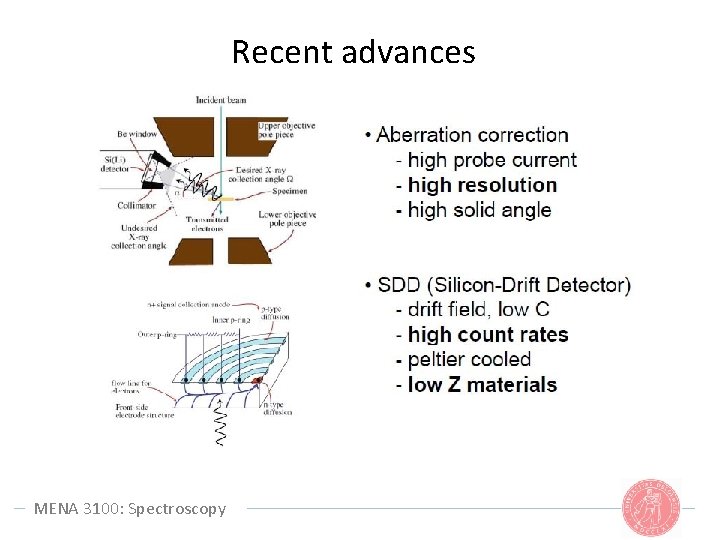
Recent advances MENA 3100: Spectroscopy

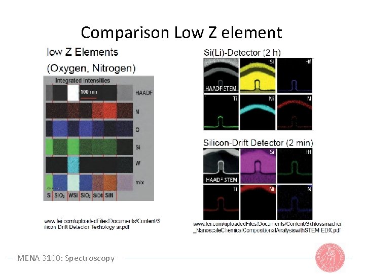
Comparison Low Z element MENA 3100: Spectroscopy

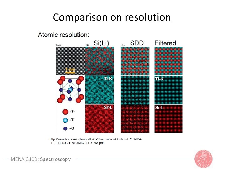
Comparison on resolution MENA 3100: Spectroscopy

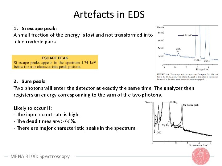
Artefacts in EDS 1. Si escape peak: A small fraction of the energy is lost and not transformed into electronhole pairs 2. Sum peak: Two photons will enter the detector at exactly the same time. The analyzer then registers an energy corresponding to the sum of the two photons. Likely to occur if: - The input count rate is high. - The dead times are > 60%. - There are major characteristic peaks in the spectrum. MENA 3100: Spectroscopy

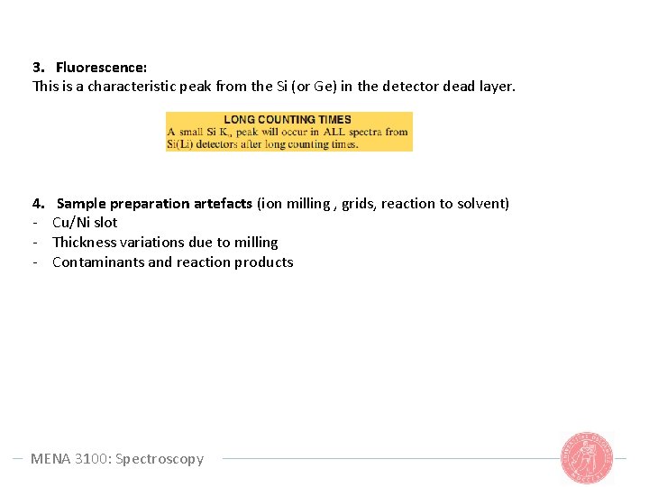
3. Fluorescence: This is a characteristic peak from the Si (or Ge) in the detector dead layer. 4. - Sample preparation artefacts (ion milling , grids, reaction to solvent) Cu/Ni slot Thickness variations due to milling Contaminants and reaction products MENA 3100: Spectroscopy

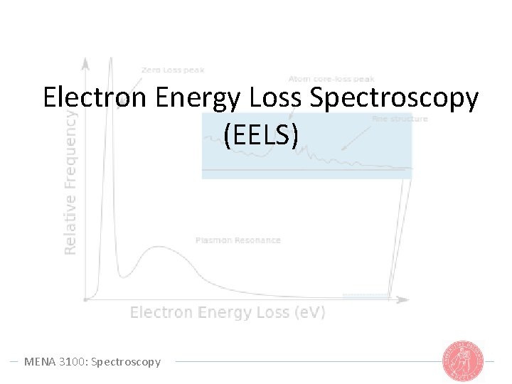
Electron Energy Loss Spectroscopy (EELS) MENA 3100: Spectroscopy

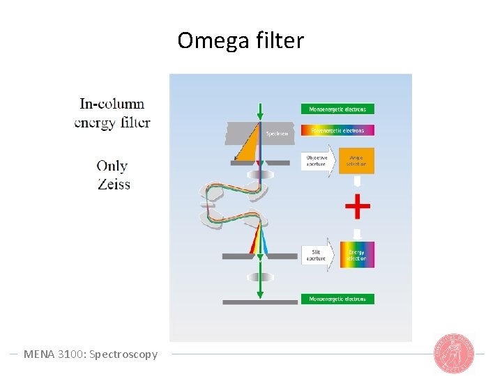
Omega filter MENA 3100: Spectroscopy

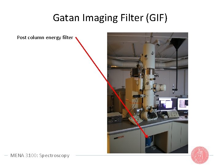
Gatan Imaging Filter (GIF) Post column energy filter MENA 3100: Spectroscopy

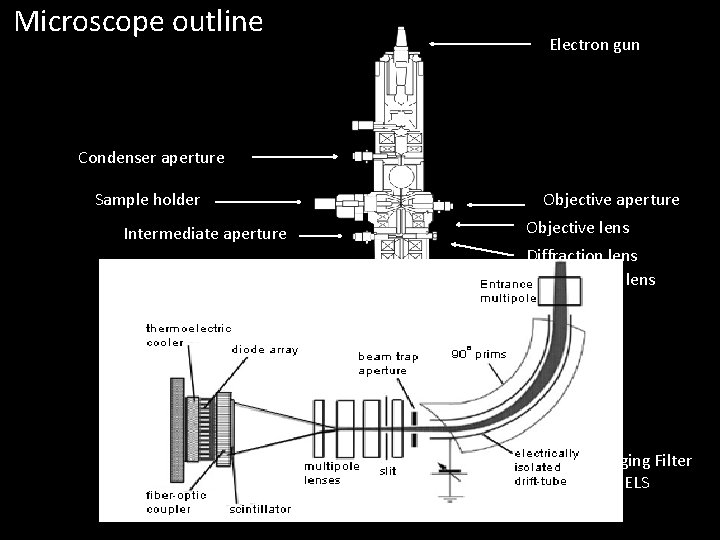
Microscope outline Electron gun Condenser aperture Sample holder Intermediate aperture Projector lenses Objective aperture Objective lens Diffraction lens Intermediate lens Fluorescent screen Gatan Imaging Filter For EELS

MENA 3100: Spectroscopy

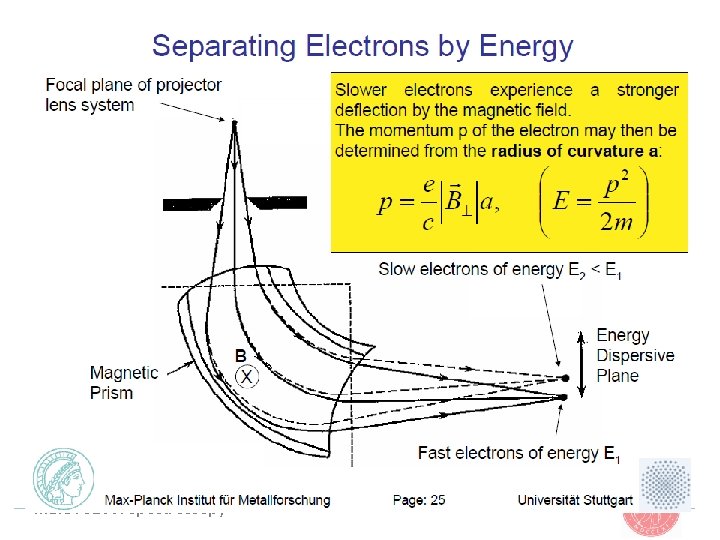
Projector crossover Viewing screen Slit Detector Multipole lenses 90 o magnetic prism Beam trap aperture

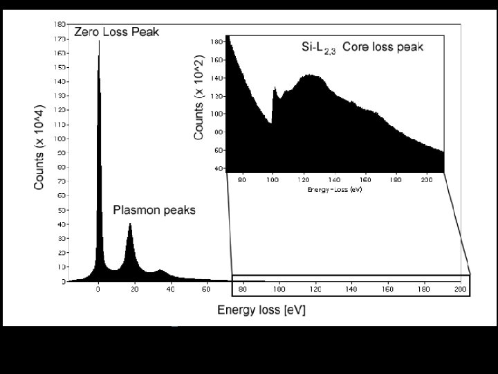
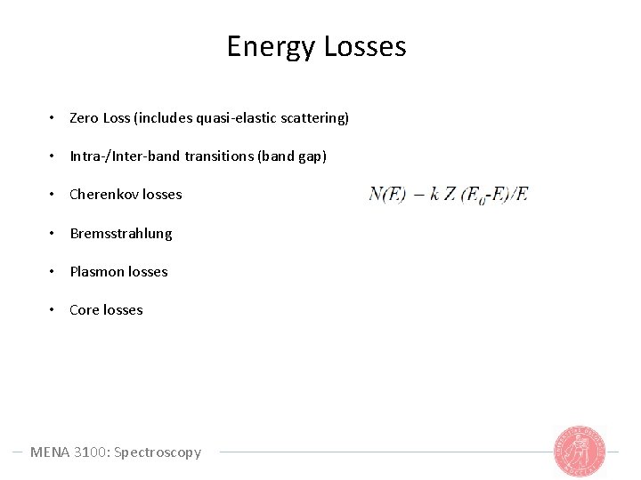
Energy Losses • Zero Loss (includes quasi-elastic scattering) • Intra-/Inter-band transitions (band gap) • Cherenkov losses • Bremsstrahlung • Plasmon losses • Core losses MENA 3100: Spectroscopy

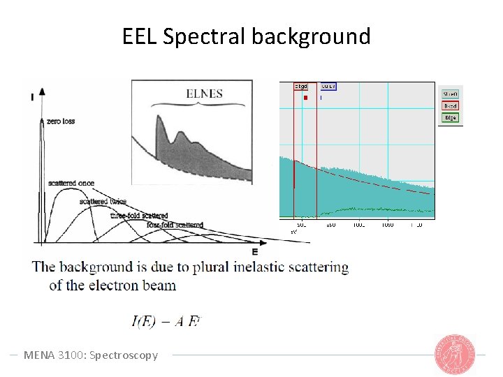
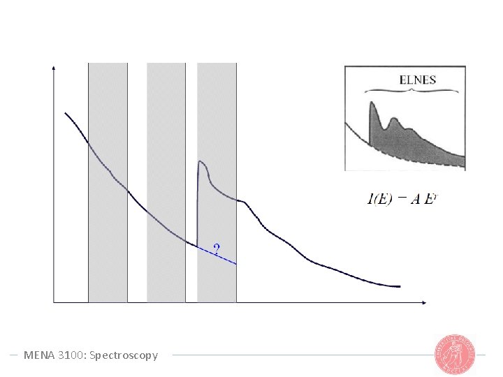
EEL Spectral background MENA 3100: Spectroscopy

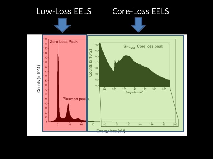
Low-Loss EELS Core-Loss EELS

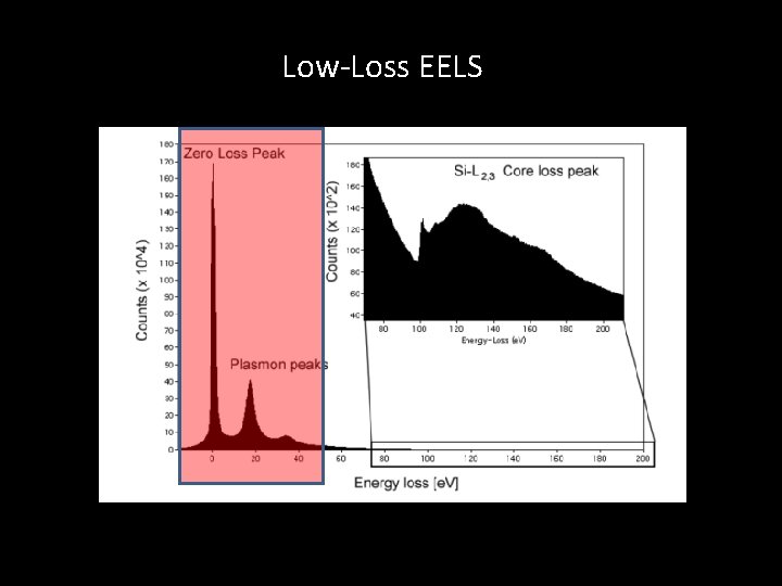
Low-Loss EELS

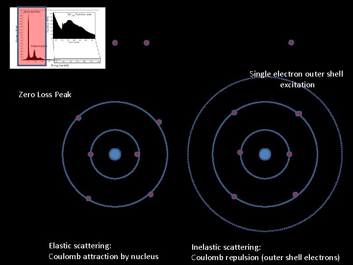
Zero Loss Peak Elastic scattering: Coulomb attraction by nucleus Single electron outer shell excitation Inelastic scattering: Coulomb repulsion (outer shell electrons)

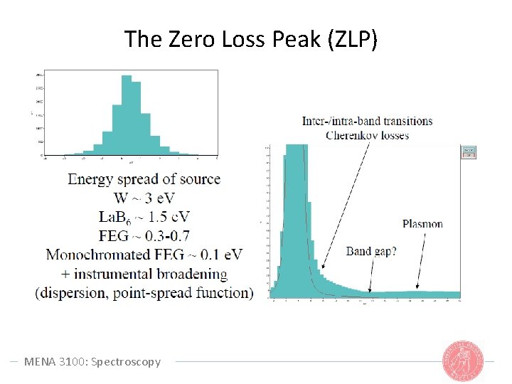
The Zero Loss Peak (ZLP) MENA 3100: Spectroscopy

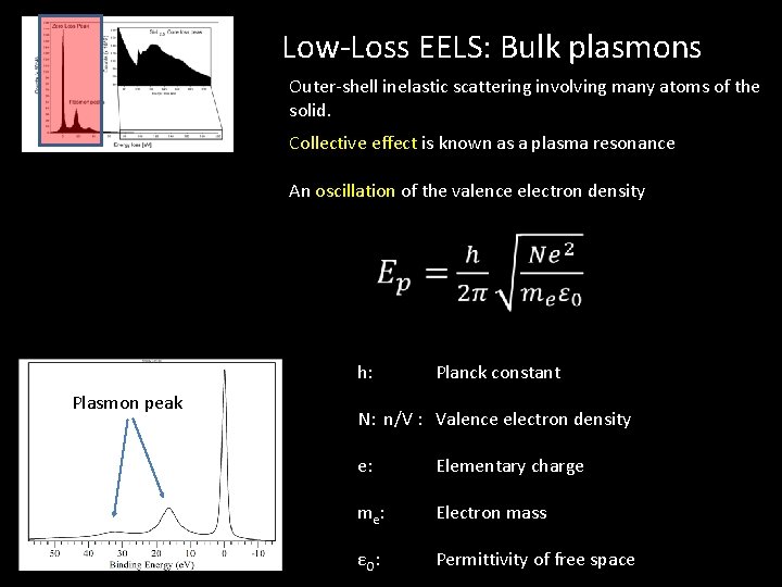
Low-Loss EELS: Bulk plasmons Outer-shell inelastic scattering involving many atoms of the solid. Collective effect is known as a plasma resonance An oscillation of the valence electron density h: Plasmon peak Planck constant N: n/V : Valence electron density e: Elementary charge me: Electron mass εO: Permittivity of free space

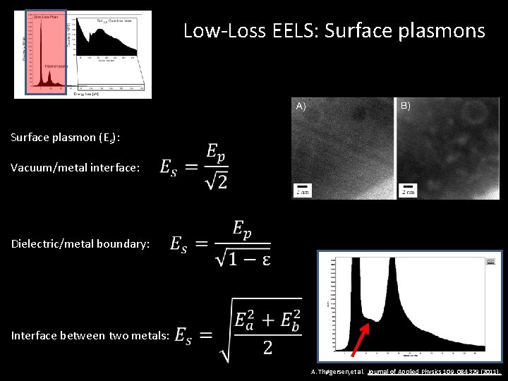
Low-Loss EELS: Surface plasmons Surface plasmon (Es): Vacuum/metal interface: ZLP Dielectric/metal boundary: Interface between two metals: A. Thøgersen, et al. Journal of Applied Physics 109, 084329 (2011).

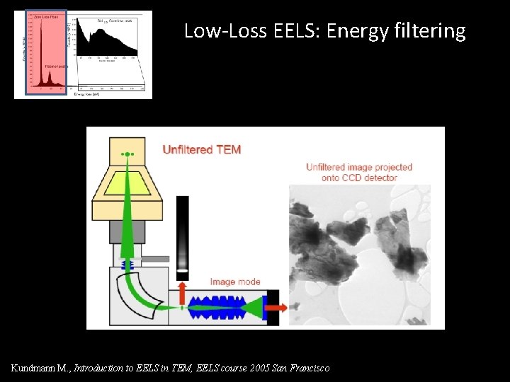
Low-Loss EELS: Energy filtering Kundmann M. , Introduction to EELS in TEM, EELS course 2005 San Francisco

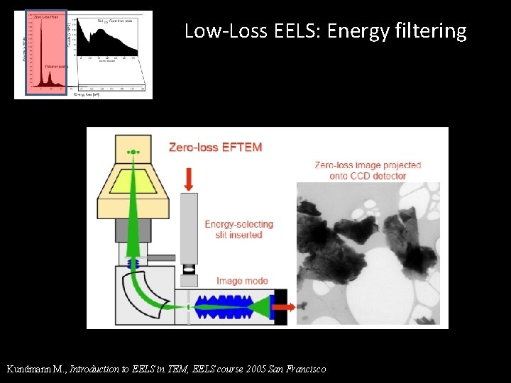
Low-Loss EELS: Energy filtering Kundmann M. , Introduction to EELS in TEM, EELS course 2005 San Francisco

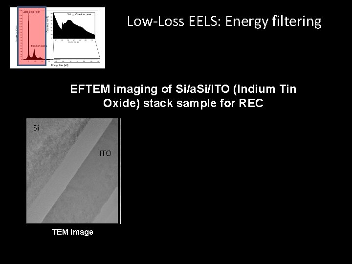
Low-Loss EELS: Energy filtering EFTEM imaging of Si/a. Si/ITO (Indium Tin Oxide) stack sample for REC Si ITO TEM image

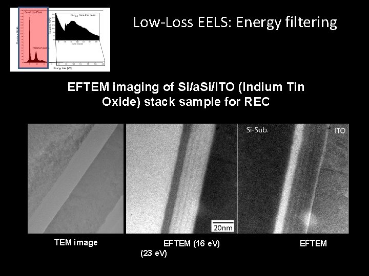
Low-Loss EELS: Energy filtering EFTEM imaging of Si/a. Si/ITO (Indium Tin Oxide) stack sample for REC TEM image EFTEM (16 e. V) (23 e. V) EFTEM

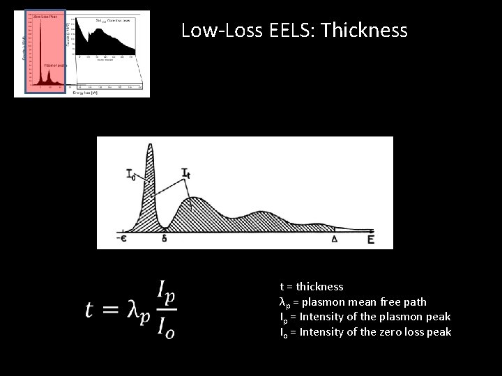
Low-Loss EELS: Thickness t = thickness λp = plasmon mean free path Ip = Intensity of the plasmon peak Io = Intensity of the zero loss peak

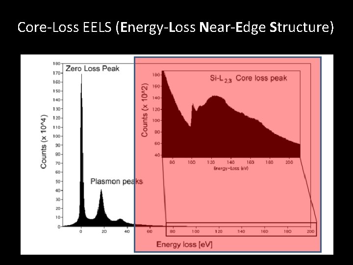
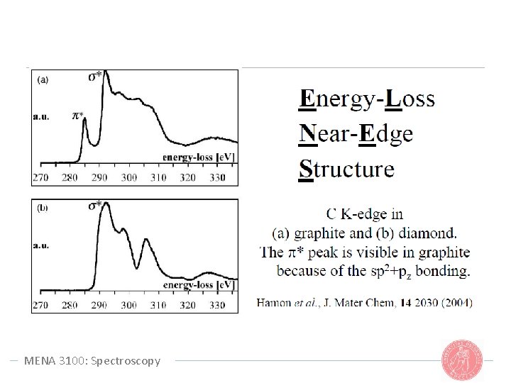
Core-Loss EELS (Energy-Loss Near-Edge Structure)

Eo Eo K-edge (Si) – 1 s orbital L-edge (Si) – 2 s and 2 p orbital M L K Filled bands Conduction band Eb(L)=Eo-Eb(cond. band-L) Eb(K)=Eo-E(cond. band-K)

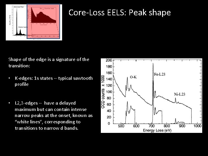
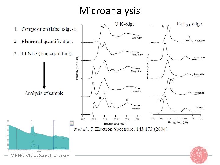
Core-Loss EELS: Peak shape Shape of the edge is a signature of the transition: • K-edges: 1 s states -- typical sawtooth profile • L 2, 3 -edges -- have a delayed maximum but can contain intense narrow peaks at the onset, known as “white lines”, corresponding to transitions to narrow d bands.

MENA 3100: Spectroscopy

Microanalysis MENA 3100: Spectroscopy

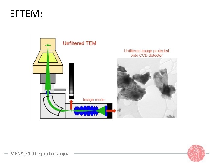
EFTEM: MENA 3100: Spectroscopy

MENA 3100: Spectroscopy

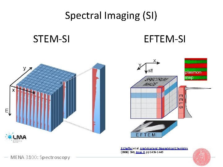
Spectral Imaging (SI) STEM-SI MENA 3100: Spectroscopy EFTEM-SI B. Chaffer et al. Analytical and Bioanalytical Chemistry (2008) 390, Issue 6, pp 1439 -1445

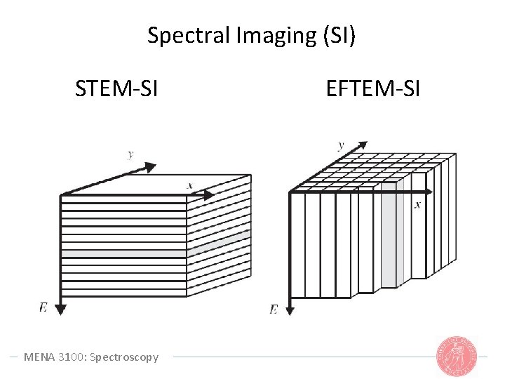
Spectral Imaging (SI) STEM-SI MENA 3100: Spectroscopy EFTEM-SI

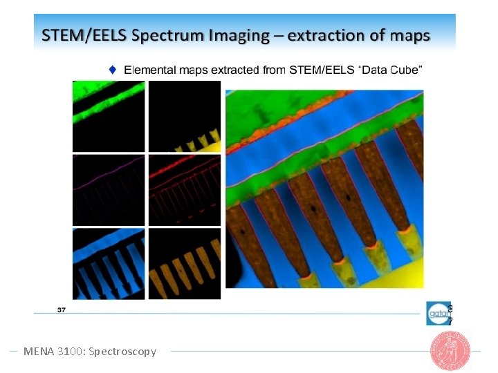
MENA 3100: Spectroscopy

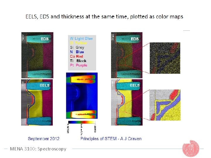
MENA 3100: Spectroscopy

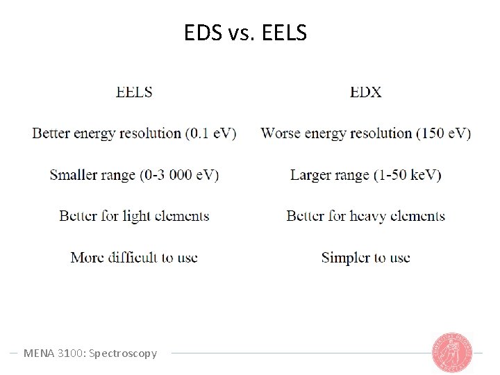
EDS vs. EELS MENA 3100: Spectroscopy

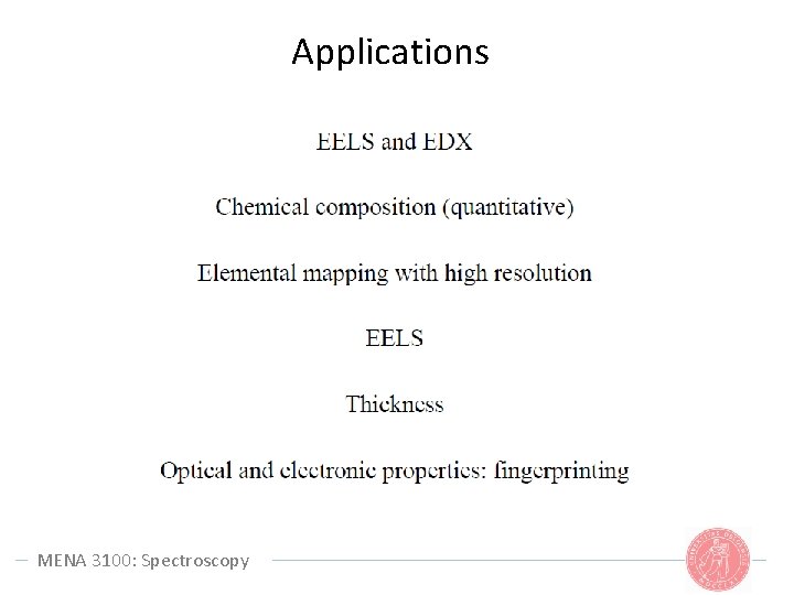
Applications MENA 3100: Spectroscopy