Analogue InputOutput n Many sensorstransducers produce voltages representing
- Slides: 12

Analogue Input/Output n Many sensors/transducers produce voltages representing physical data. ¨ To process transducer data in a computer requires conversion to digital form. Examples: n n n reading temperature from a thermocouple processing speech from a microphone Many output devices require variable control, not just two digital logic levels ¨ To control these devices from a computer requires conversion from digital to analogue form. 1

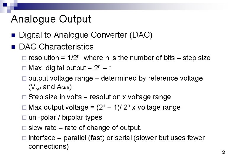
Analogue Output n n Digital to Analogue Converter (DAC) DAC Characteristics ¨ resolution = 1/2 n where n is the number of bits – step size ¨ Max. digital output = 2 n – 1 ¨ output voltage range – determined by reference voltage (Vref and AGND) ¨ Step size in volts = resolution x voltage range ¨ Max output voltage = (2 n – 1)/ 2 n x voltage range ¨ uni-polar / bipolar types ¨ slew rate – rate of change of output. ¨ interface – parallel (fast) or serial (slower but uses fewer connections) 2

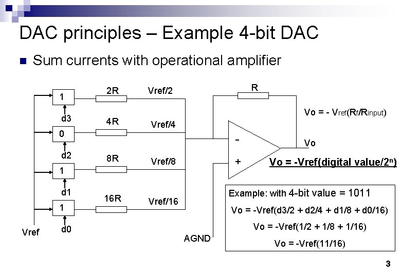
DAC principles – Example 4 -bit DAC n Sum currents with operational amplifier 1 d 3 2 R 4 R 0 d 2 1 Vref d 0 Vo = - Vref(Rf/Rinput) Vref/4 8 R 1 d 1 R Vref/2 16 R Vref/8 + Vo Vo = -Vref(digital value/2 n) Example: with 4 -bit value = 1011 Vref/16 Vo = -Vref(d 3/2 + d 2/4 + d 1/8 + d 0/16) Vo = -Vref(1/2 + 1/8 + 1/16) AGND Vo = -Vref(11/16) 3

Digital to Analogue conversion n Previous design needs many different precise resistor values Resisters need to have a tolerance less than the resolution. E. g. 8 -bit resolution = 1: 28 = 1/256 = 0. 00390625 resolution = 0. 390625% Alternative is R-2 R ladder arrangement ¨ R-2 R ladder - only requires 2 different resistor values. 4

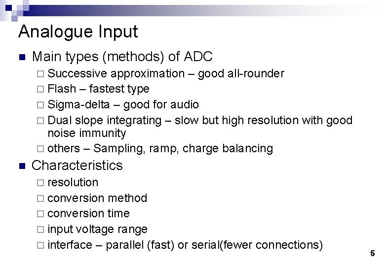
Analogue Input n Main types (methods) of ADC ¨ Successive approximation – good all-rounder ¨ Flash – fastest type ¨ Sigma-delta – good for audio ¨ Dual slope integrating – slow but high resolution with good noise immunity ¨ others – Sampling, ramp, charge balancing n Characteristics ¨ resolution ¨ conversion method ¨ conversion time ¨ input voltage range ¨ interface – parallel (fast) or serial(fewer connections) 5

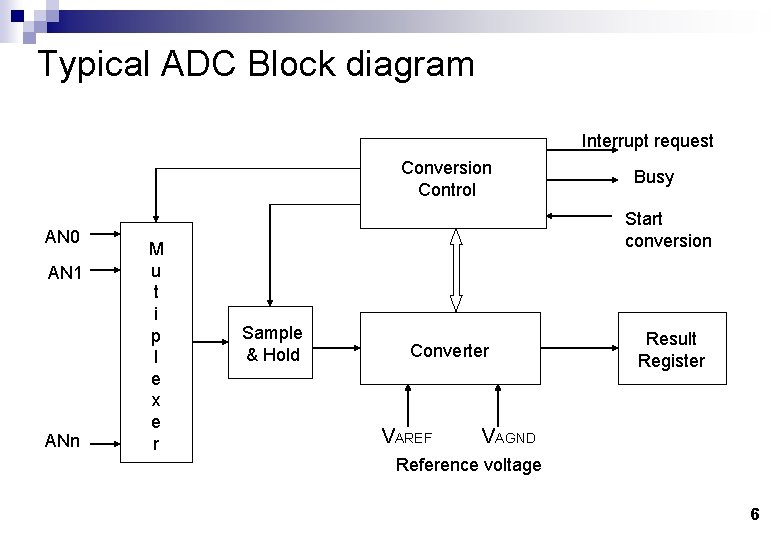
Typical ADC Block diagram Interrupt request Conversion Control AN 0 AN 1 ANn M u t i p l e x e r Busy Start conversion Sample & Hold Converter VAREF Result Register VAGND Reference voltage 6

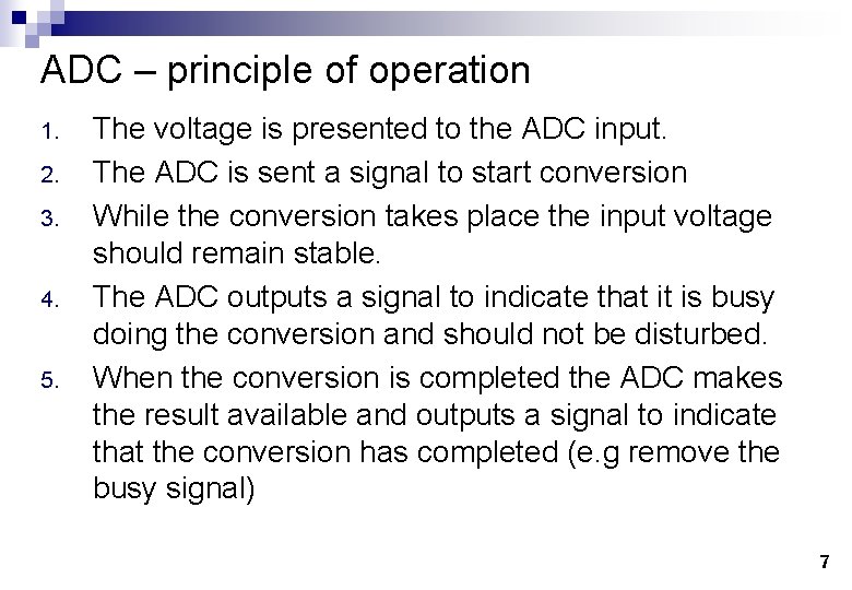
ADC – principle of operation 1. 2. 3. 4. 5. The voltage is presented to the ADC input. The ADC is sent a signal to start conversion While the conversion takes place the input voltage should remain stable. The ADC outputs a signal to indicate that it is busy doing the conversion and should not be disturbed. When the conversion is completed the ADC makes the result available and outputs a signal to indicate that the conversion has completed (e. g remove the busy signal) 7

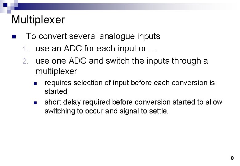
Multiplexer n To convert several analogue inputs 1. use an ADC for each input or … 2. use one ADC and switch the inputs through a multiplexer n n requires selection of input before each conversion is started short delay required before conversion started to allow switching to occur and signal to settle. 8

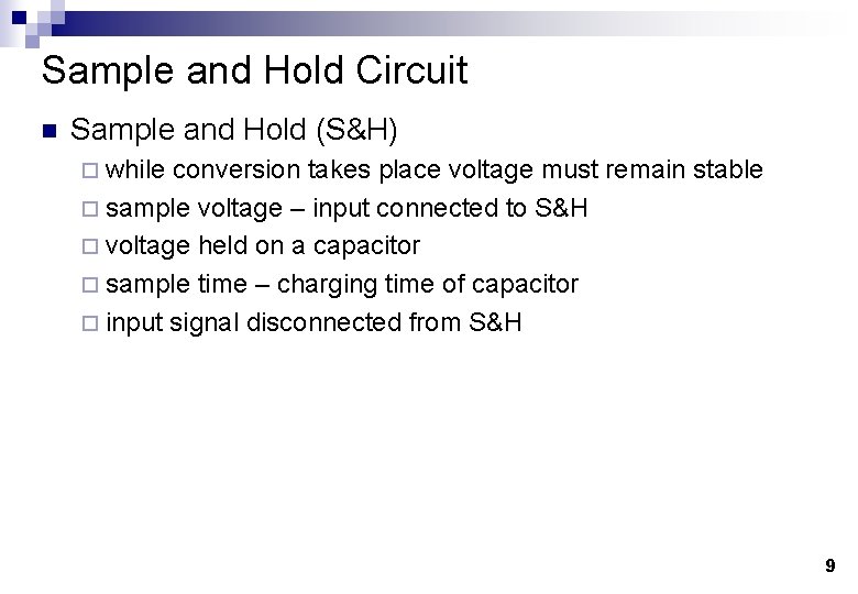
Sample and Hold Circuit n Sample and Hold (S&H) ¨ while conversion takes place voltage must remain stable ¨ sample voltage – input connected to S&H ¨ voltage held on a capacitor ¨ sample time – charging time of capacitor ¨ input signal disconnected from S&H 9

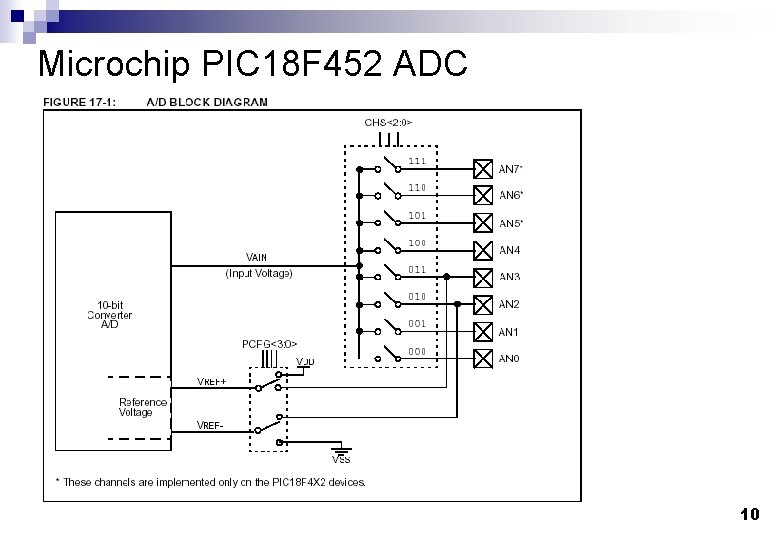
Microchip PIC 18 F 452 ADC 10

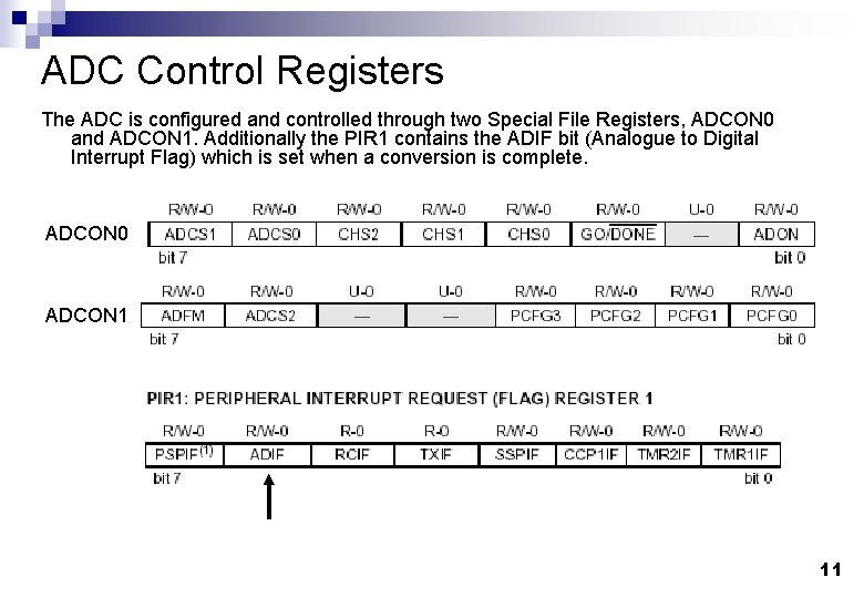
ADC Control Registers The ADC is configured and controlled through two Special File Registers, ADCON 0 and ADCON 1. Additionally the PIR 1 contains the ADIF bit (Analogue to Digital Interrupt Flag) which is set when a conversion is complete. ADCON 0 ADCON 1 11

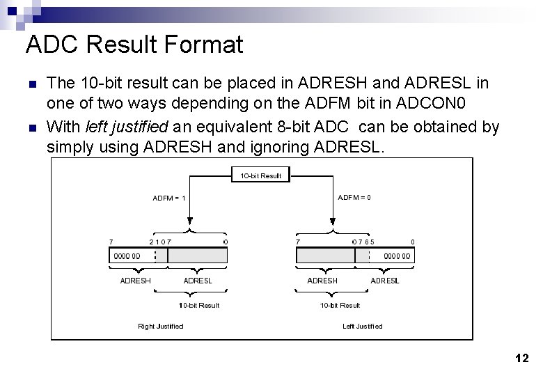
ADC Result Format n n The 10 -bit result can be placed in ADRESH and ADRESL in one of two ways depending on the ADFM bit in ADCON 0 With left justified an equivalent 8 -bit ADC can be obtained by simply using ADRESH and ignoring ADRESL. 12