Analog Interfacing ARM University Program Copyright ARM Ltd

![DAC Data Registers § These registers are only eight bits long § DATA[11: 0] DAC Data Registers § These registers are only eight bits long § DATA[11: 0]](https://slidetodoc.com/presentation_image/5c72899e83918ed1ad2c9b7a41650aeb/image-30.jpg)
![Input Channel Selection § Two modes, selected by SC 1 n[DIFF] bit § § Input Channel Selection § Two modes, selected by SC 1 n[DIFF] bit § §](https://slidetodoc.com/presentation_image/5c72899e83918ed1ad2c9b7a41650aeb/image-52.jpg)
- Slides: 60

Analog Interfacing ARM University Program Copyright © ARM Ltd 2013 1

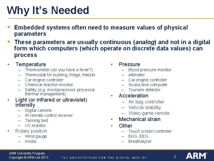
Why It’s Needed § § Embedded systems often need to measure values of physical parameters These parameters are usually continuous (analog) and not in a digital form which computers (which operate on discrete data values) can process • Temperature – – – • Light (or infrared or ultraviolet) intensity – – • Thermometer (do you have a fever? ) Thermostat for building, fridge, freezer Car engine controller Chemical reaction monitor Safety (e. g. microprocessor thermal management) Digital camera IR remote control receiver Tanning bed UV monitor Rotary position – Wind gauge – Knobs ARM University Program Copyright © ARM Ltd 2013 • Pressure – – – • Blood pressure monitor Altimeter Car engine controller Scuba dive computer Tsunami detector Acceleration – Air bag controller – Vehicle stability – Video game remote • • Mechanical strain Other – Touch screen controller – EKG, EEG – Breathalyzer 2

CONVERTING BETWEEN ANALOG AND DIGITAL VALUES ARM University Program Copyright © ARM Ltd 2013 3

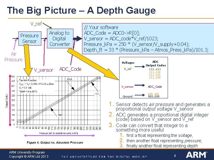
The Big Picture – A Depth Gauge V_ref Pressure Sensor Analog to Digital Converter Air Pressure // Your software ADC_Code = ADC 0 ->R[0]; V_sensor = ADC_code*V_ref/1023; Pressure_k. Pa = 250 * (V_sensor/V_supply+0. 04); Depth_ft = 33 * (Pressure_k. Pa – Atmos_Press_k. Pa)/101. 3; Voltages V_sensor ADC_Code V_ref V_sensor Ground 1. 2. 3. ADC_Code 000. . 001 000. . 000 Sensor detects air pressure and generates a proportional output voltage V_sensor ADC generates a proportional digital integer (code) based on V_sensor and V_ref Code can convert that integer to a something more useful 1. 2. 3. ARM University Program Copyright © ARM Ltd 2013 ADC Output Codes 111. . 110 111. . 101 111. . 100 first a float representing the voltage, then another float representing pressure, finally another float representing depth 4

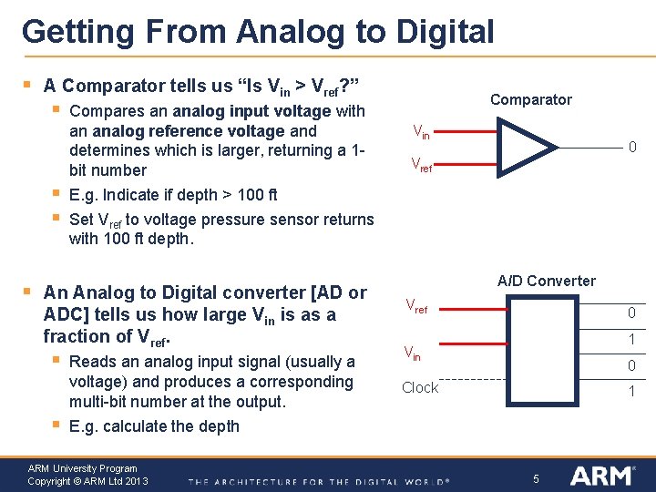
Getting From Analog to Digital § A Comparator tells us “Is Vin > Vref? ” § § Compares an analog input voltage with an analog reference voltage and determines which is larger, returning a 1 bit number E. g. Indicate if depth > 100 ft Set Vref to voltage pressure sensor returns with 100 ft depth. An Analog to Digital converter [AD or ADC] tells us how large Vin is as a fraction of Vref. § § Reads an analog input signal (usually a voltage) and produces a corresponding multi-bit number at the output. E. g. calculate the depth ARM University Program Copyright © ARM Ltd 2013 Comparator Vin 0 Vref A/D Converter Vref 0 1 Vin 0 Clock 1 5

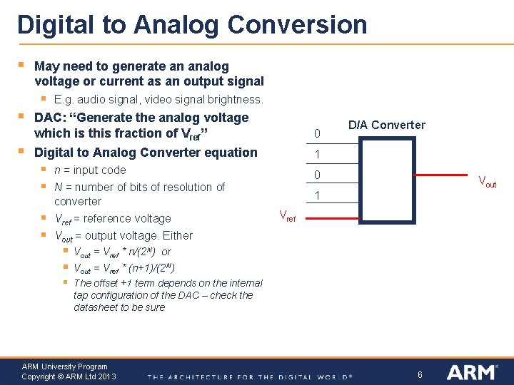
Digital to Analog Conversion § May need to generate an analog voltage or current as an output signal § § § E. g. audio signal, video signal brightness. DAC: “Generate the analog voltage which is this fraction of Vref” Digital to Analog Converter equation § § n = input code N = number of bits of resolution of converter Vref = reference voltage Vout = output voltage. Either § § § 0 D/A Converter 1 0 Vout 1 Vref Vout = Vref * n/(2 N) or Vout = Vref * (n+1)/(2 N) The offset +1 term depends on the internal tap configuration of the DAC – check the datasheet to be sure ARM University Program Copyright © ARM Ltd 2013 6

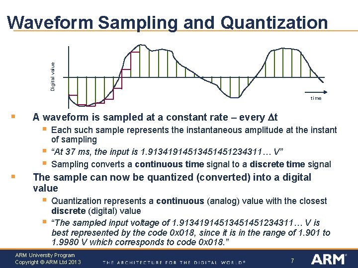
Digital value Waveform Sampling and Quantization time § § A waveform is sampled at a constant rate – every Dt § § § Each such sample represents the instantaneous amplitude at the instant of sampling “At 37 ms, the input is 1. 91341914513451451234311… V” Sampling converts a continuous time signal to a discrete time signal The sample can now be quantized (converted) into a digital value § § Quantization represents a continuous (analog) value with the closest discrete (digital) value “The sampled input voltage of 1. 91341914513451451234311… V is best represented by the code 0 x 018, since it is in the range of 1. 901 to 1. 9980 V which corresponds to code 0 x 018. ” ARM University Program Copyright © ARM Ltd 2013 7

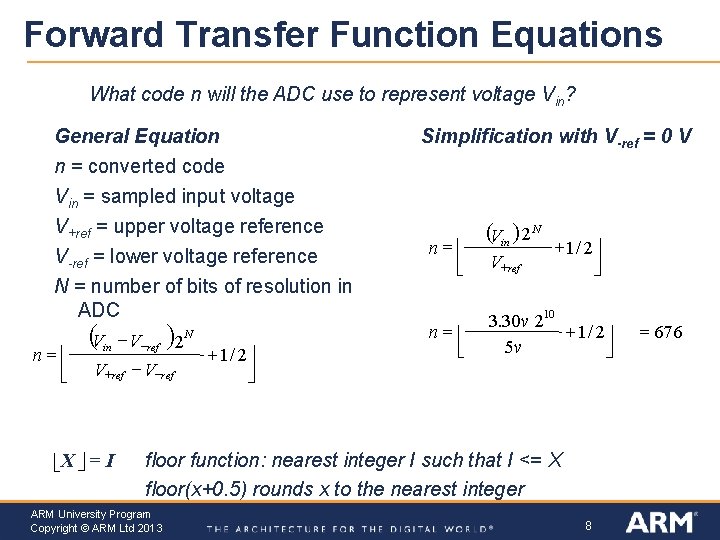
Forward Transfer Function Equations What code n will the ADC use to represent voltage Vin? General Equation n = converted code Simplification with V-ref = 0 V Vin = sampled input voltage V+ref = upper voltage reference V-ref = lower voltage reference N = number of bits of resolution in ADC n=ê êë (V in - V-ref ) 2 N V+ ref - V-ref ëX û = I + 1/ 2ú úû n=ê êë n=ê ë (Vin ) 2 N V+ ref + 1/ 2ú úû 3. 30 v 210 + 1 / 2ú 5 v û floor function: nearest integer I such that I <= X floor(x+0. 5) rounds x to the nearest integer ARM University Program Copyright © ARM Ltd 2013 8 = 676

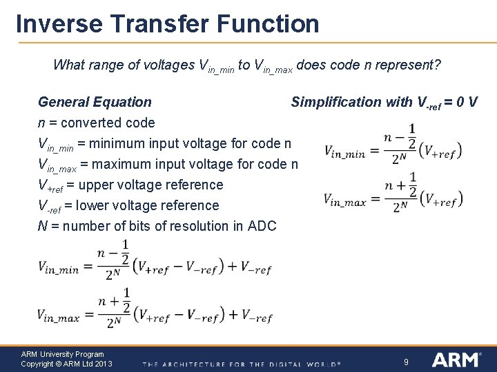
Inverse Transfer Function What range of voltages Vin_min to Vin_max does code n represent? General Equation n = converted code Simplification with V-ref = 0 V Vin_min = minimum input voltage for code n Vin_max = maximum input voltage for code n V+ref = upper voltage reference V-ref = lower voltage reference N = number of bits of resolution in ADC ARM University Program Copyright © ARM Ltd 2013 9

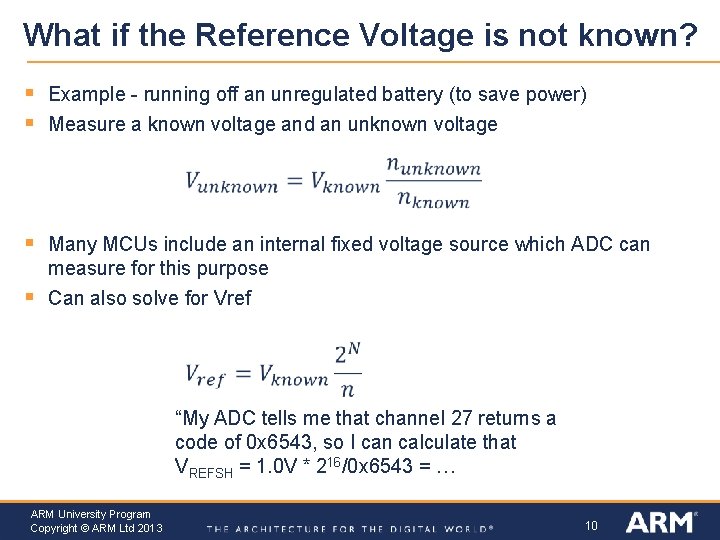
What if the Reference Voltage is not known? § § Example - running off an unregulated battery (to save power) Measure a known voltage and an unknown voltage § § Many MCUs include an internal fixed voltage source which ADC can measure for this purpose Can also solve for Vref “My ADC tells me that channel 27 returns a code of 0 x 6543, so I can calculate that VREFSH = 1. 0 V * 216/0 x 6543 = … ARM University Program Copyright © ARM Ltd 2013 10

ANALOG TO DIGITAL CONVERSION CONCEPTS ARM University Program Copyright © ARM Ltd 2013 11

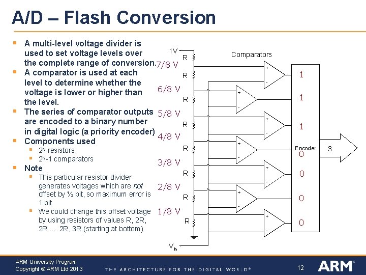
A/D – Flash Conversion § § § A multi-level voltage divider is 1 V used to set voltage levels over R the complete range of conversion. 7/8 V A comparator is used at each R level to determine whether the 6/8 V voltage is lower or higher than R the level. The series of comparator outputs 5/8 V are encoded to a binary number R in digital logic (a priority encoder) 4/8 V Components used § § 2 N resistors 2 N-1 comparators Note § § R Comparators + + 1 + + 0 + R This particular resistor divider generates voltages which are not 2/8 V offset by ½ bit, so maximum error is R 1 bit We could change this offset voltage 1/8 V by using resistors of values R, 2 R, R 2 R. . . 2 R, 3 R (starting at bottom) 1 Encoder - 3/8 V 1 0 + 0 - Vin ARM University Program Copyright © ARM Ltd 2013 12 3

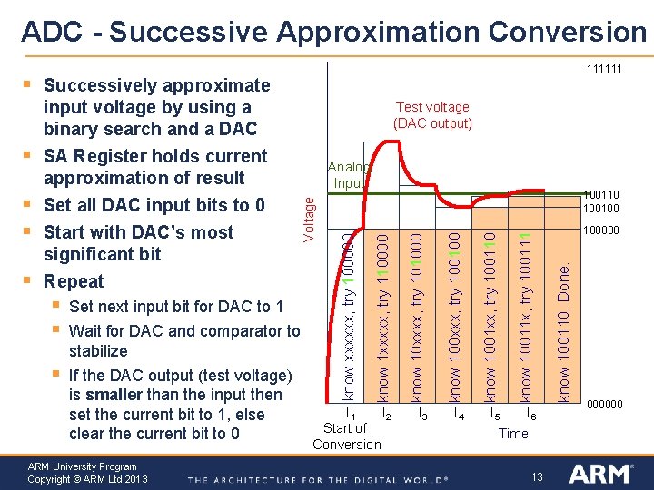
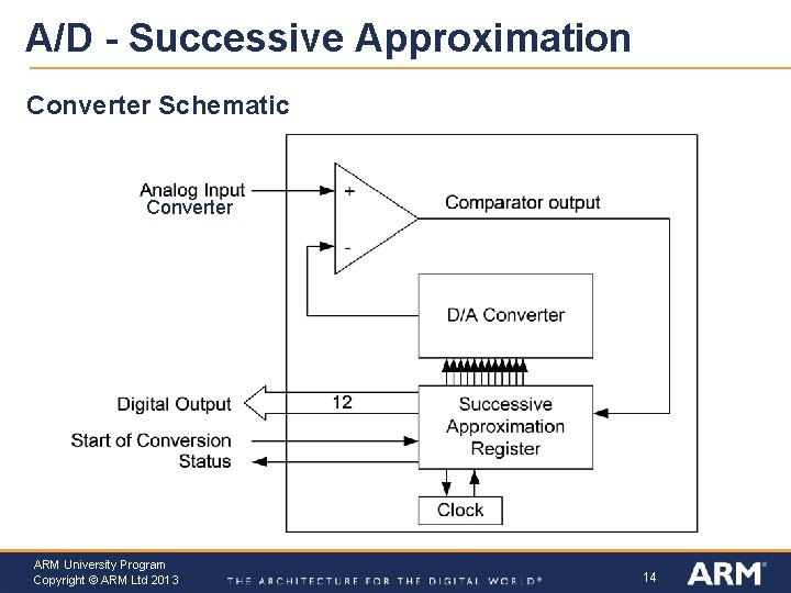
ADC - Successive Approximation Conversion ARM University Program Copyright © ARM Ltd 2013 know 10011 x, try 100111 T 2 Start of Conversion T 3 T 4 T 5 T 6 Time 13 100000 know 100110. Done. know 1001 xx, try 100110 § Set next input bit for DAC to 1 Wait for DAC and comparator to stabilize If the DAC output (test voltage) is smaller than the input then set the current bit to 1, else clear the current bit to 0 know 100 xxx, try 100100 § § 100110 100100 know 10 xxxx, try 101000 § Analog Input know 1 xxxxx, try 110000 § § Test voltage (DAC output) know xxxxxx, try 100000 § Successively approximate input voltage by using a binary search and a DAC SA Register holds current approximation of result Set all DAC input bits to 0 Start with DAC’s most significant bit Repeat Voltage § 111111 000000

A/D - Successive Approximation Converter Schematic Converter ARM University Program Copyright © ARM Ltd 2013 14

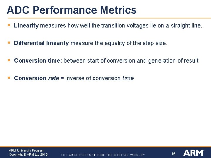
ADC Performance Metrics § Linearity measures how well the transition voltages lie on a straight line. § Differential linearity measure the equality of the step size. § Conversion time: between start of conversion and generation of result § Conversion rate = inverse of conversion time ARM University Program Copyright © ARM Ltd 2013 15

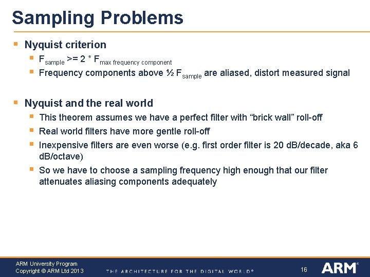
Sampling Problems § Nyquist criterion § § § Fsample >= 2 * Fmax frequency component Frequency components above ½ Fsample are aliased, distort measured signal Nyquist and the real world § § This theorem assumes we have a perfect filter with “brick wall” roll-off Real world filters have more gentle roll-off Inexpensive filters are even worse (e. g. first order filter is 20 d. B/decade, aka 6 d. B/octave) So we have to choose a sampling frequency high enough that our filter attenuates aliasing components adequately ARM University Program Copyright © ARM Ltd 2013 16

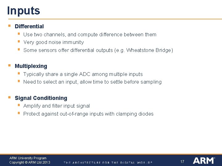
Inputs § Differential § § Multiplexing § § § Use two channels, and compute difference between them Very good noise immunity Some sensors offer differential outputs (e. g. Wheatstone Bridge) Typically share a single ADC among multiple inputs Need to select an input, allow time to settle before sampling Signal Conditioning § § Amplify and filter input signal Protect against out-of-range inputs with clamping diodes ARM University Program Copyright © ARM Ltd 2013 17

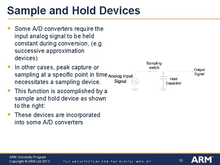
Sample and Hold Devices § § Some A/D converters require the input analog signal to be held constant during conversion, (e. g. successive approximation devices) In other cases, peak capture or sampling at a specific point in time necessitates a sampling device. This function is accomplished by a sample and hold device as shown to the right: These devices are incorporated into some A/D converters ARM University Program Copyright © ARM Ltd 2013 18

KL 25 ANALOG INTERFACING PERIPHERALS ARM University Program Copyright © ARM Ltd 2013 19

Sources of Information § KL 25 Subfamily Reference Manual (Rev. 1, June 2012) § § Describes architecture of peripherals and their control registers Digital to Analog Converter § § Analog Comparator § § Chapter 29 of KL 25 Subfamily Reference Manual Analog to Digital Converter § § Chapter 30 of KL 25 Subfamily Reference Manual Chapter 28 of KL 25 Subfamily Reference Manual KL 25 Sub-family Data Sheet (Rev. 3, 9/19/2012) § Describes circuit-specific performance parameters: operating voltages, min/max speeds, cycle times, delays, power and energy use ARM University Program Copyright © ARM Ltd 2013 20

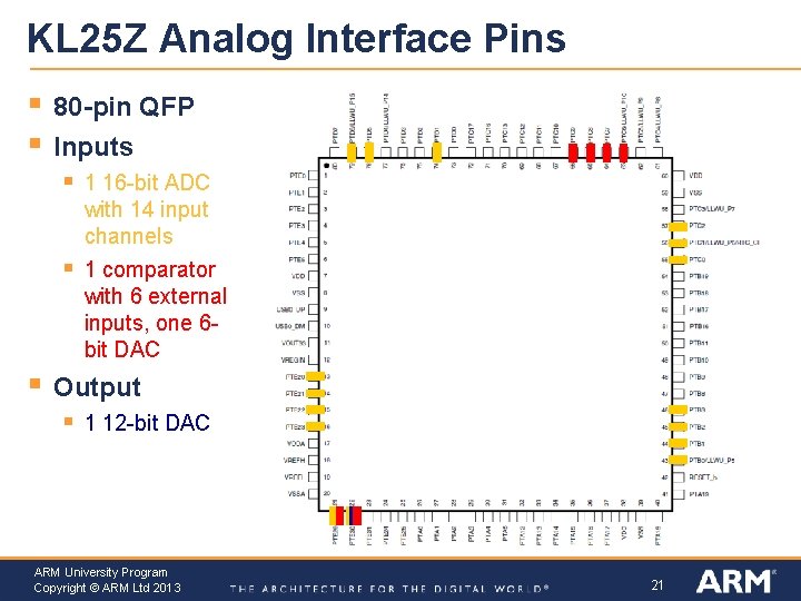
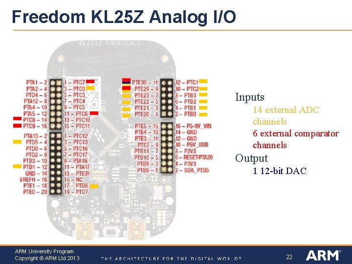
KL 25 Z Analog Interface Pins § § 80 -pin QFP Inputs § § § 1 16 -bit ADC with 14 input channels 1 comparator with 6 external inputs, one 6 bit DAC Output § 1 12 -bit DAC ARM University Program Copyright © ARM Ltd 2013 21

Freedom KL 25 Z Analog I/O Inputs 14 external ADC channels 6 external comparator channels Output 1 12 -bit DAC ARM University Program Copyright © ARM Ltd 2013 22

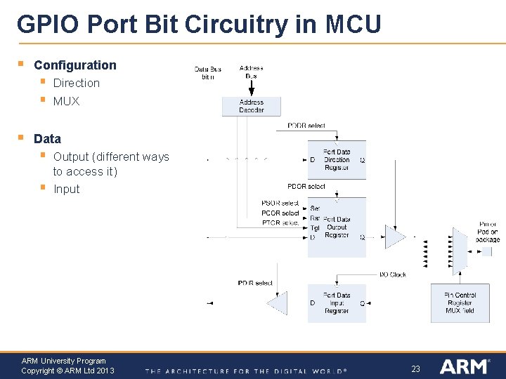
GPIO Port Bit Circuitry in MCU § Configuration § § § Direction MUX Data § § Output (different ways to access it) Input ARM University Program Copyright © ARM Ltd 2013 23

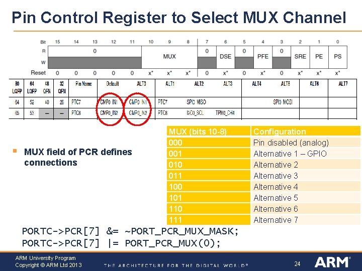
Pin Control Register to Select MUX Channel § MUX field of PCR defines connections MUX (bits 10 -8) 000 001 010 011 100 101 110 111 Configuration Pin disabled (analog) Alternative 1 – GPIO Alternative 2 Alternative 3 Alternative 4 Alternative 5 Alternative 6 Alternative 7 PORTC->PCR[7] &= ~PORT_PCR_MUX_MASK; PORTC->PCR[7] |= PORT_PCR_MUX(0); ARM University Program Copyright © ARM Ltd 2013 24

DIGITAL TO ANALOG CONVERTER ARM University Program Copyright © ARM Ltd 2013 25

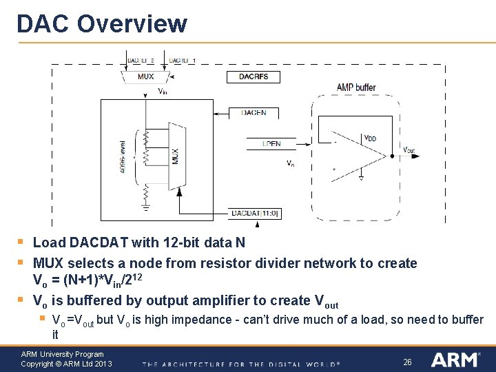
DAC Overview § § § Load DACDAT with 12 -bit data N MUX selects a node from resistor divider network to create Vo = (N+1)*Vin/212 Vo is buffered by output amplifier to create Vout § Vo =Vout but Vo is high impedance - can’t drive much of a load, so need to buffer it ARM University Program Copyright © ARM Ltd 2013 26

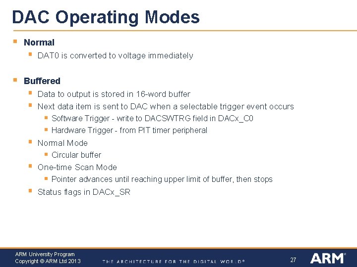
DAC Operating Modes § Normal § § DAT 0 is converted to voltage immediately Buffered § § Data to output is stored in 16 -word buffer Next data item is sent to DAC when a selectable trigger event occurs § § § Normal Mode § § Circular buffer One-time Scan Mode § § Software Trigger - write to DACSWTRG field in DACx_C 0 Hardware Trigger - from PIT timer peripheral Pointer advances until reaching upper limit of buffer, then stops Status flags in DACx_SR ARM University Program Copyright © ARM Ltd 2013 27

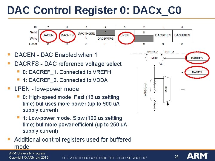
DAC Control Register 0: DACx_C 0 § § DACEN - DAC Enabled when 1 DACRFS - DAC reference voltage select § § § 1: DACREF_2. Connected to VDDA LPEN - low-power mode § § § 0: DACREF_1. Connected to VREFH 0: High-speed mode. Fast (15 us settling time) but uses more power (up to 900 u. A supply current) 1: Low-power mode. Slow (100 us settling time) but more power-efficient (up to 250 u. A supply current) Additional control registers used for buffered mode ARM University Program Copyright © ARM Ltd 2013 28

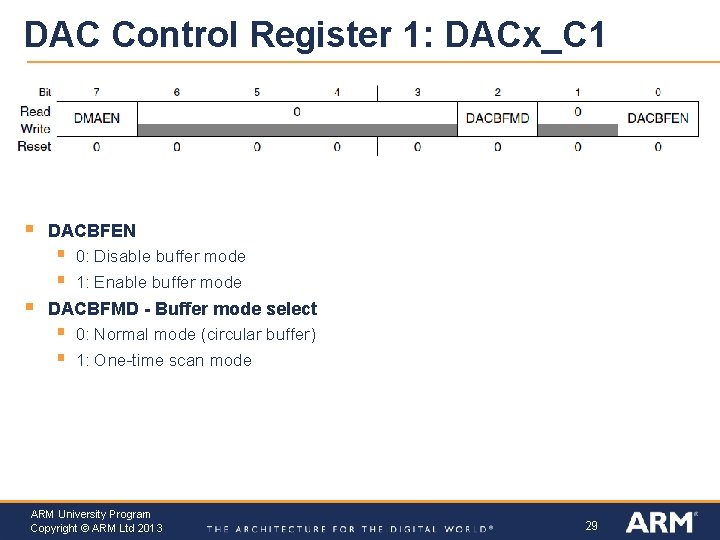
DAC Control Register 1: DACx_C 1 § DACBFEN § § § 0: Disable buffer mode 1: Enable buffer mode DACBFMD - Buffer mode select § § 0: Normal mode (circular buffer) 1: One-time scan mode ARM University Program Copyright © ARM Ltd 2013 29
![DAC Data Registers These registers are only eight bits long DATA11 0 DAC Data Registers § These registers are only eight bits long § DATA[11: 0]](https://slidetodoc.com/presentation_image/5c72899e83918ed1ad2c9b7a41650aeb/image-30.jpg)
DAC Data Registers § These registers are only eight bits long § DATA[11: 0] stored in two registers § § DATA 0: Low byte [7: 0] in DACx_DATn. L DATA 1: High nibble [11: 0] in DACx_DATn. H ARM University Program Copyright © ARM Ltd 2013 30

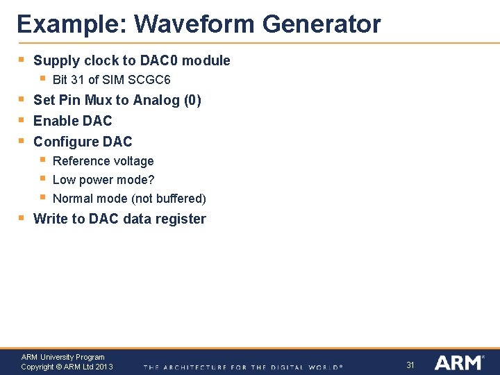
Example: Waveform Generator § Supply clock to DAC 0 module § § Set Pin Mux to Analog (0) Enable DAC Configure DAC § § Bit 31 of SIM SCGC 6 Reference voltage Low power mode? Normal mode (not buffered) Write to DAC data register ARM University Program Copyright © ARM Ltd 2013 31

ANALOG COMPARATOR ARM University Program Copyright © ARM Ltd 2013 32

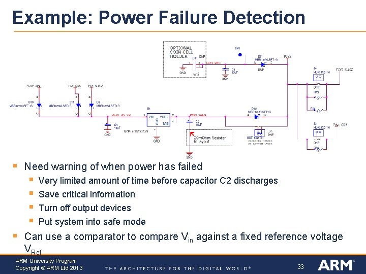
Example: Power Failure Detection § Need warning of when power has failed § § § Very limited amount of time before capacitor C 2 discharges Save critical information Turn off output devices Put system into safe mode Can use a comparator to compare Vin against a fixed reference voltage VRef ARM University Program Copyright © ARM Ltd 2013 33

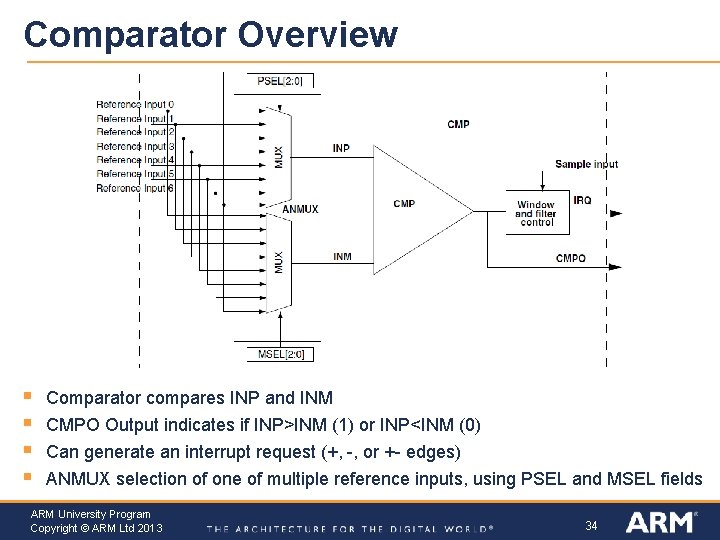
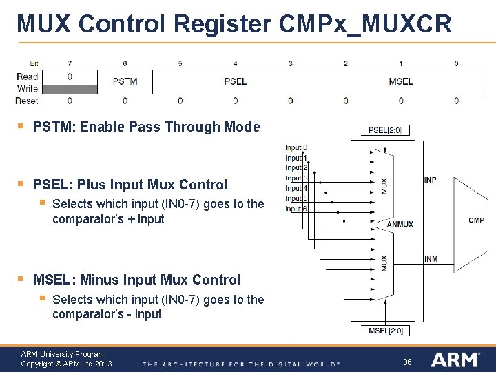
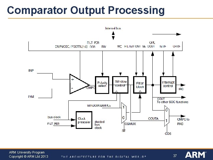
Comparator Overview § § Comparator compares INP and INM CMPO Output indicates if INP>INM (1) or INP<INM (0) Can generate an interrupt request (+, -, or +- edges) ANMUX selection of one of multiple reference inputs, using PSEL and MSEL fields ARM University Program Copyright © ARM Ltd 2013 34

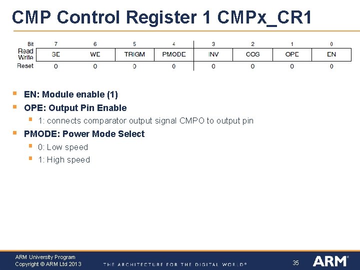
CMP Control Register 1 CMPx_CR 1 § § EN: Module enable (1) OPE: Output Pin Enable § § 1: connects comparator output signal CMPO to output pin PMODE: Power Mode Select § § 0: Low speed 1: High speed ARM University Program Copyright © ARM Ltd 2013 35

MUX Control Register CMPx_MUXCR § PSTM: Enable Pass Through Mode § PSEL: Plus Input Mux Control § § Selects which input (IN 0 -7) goes to the comparator’s + input MSEL: Minus Input Mux Control § Selects which input (IN 0 -7) goes to the comparator’s - input ARM University Program Copyright © ARM Ltd 2013 36

Comparator Output Processing ARM University Program Copyright © ARM Ltd 2013 37

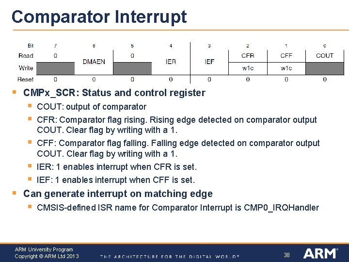
Comparator Interrupt § CMPx_SCR: Status and control register § § COUT: output of comparator CFR: Comparator flag rising. Rising edge detected on comparator output COUT. Clear flag by writing with a 1. § CFF: Comparator flag falling. Falling edge detected on comparator output COUT. Clear flag by writing with a 1. IER: 1 enables interrupt when CFR is set. IEF: 1 enables interrupt when CFF is set. § § § Can generate interrupt on matching edge § CMSIS-defined ISR name for Comparator Interrupt is CMP 0_IRQHandler ARM University Program Copyright © ARM Ltd 2013 38

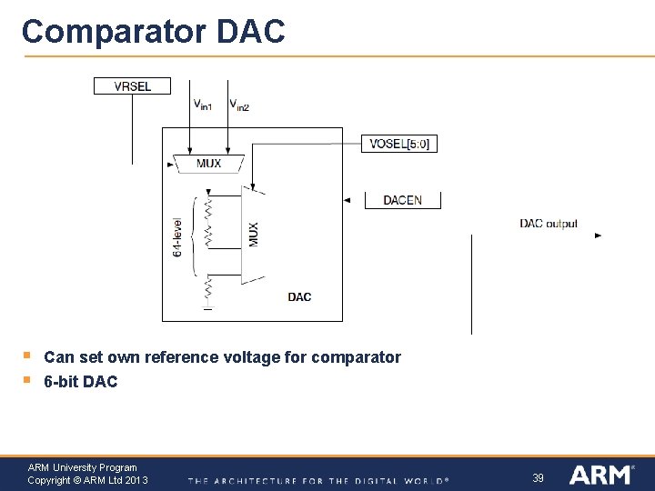
Comparator DAC § § Can set own reference voltage for comparator 6 -bit DAC ARM University Program Copyright © ARM Ltd 2013 39

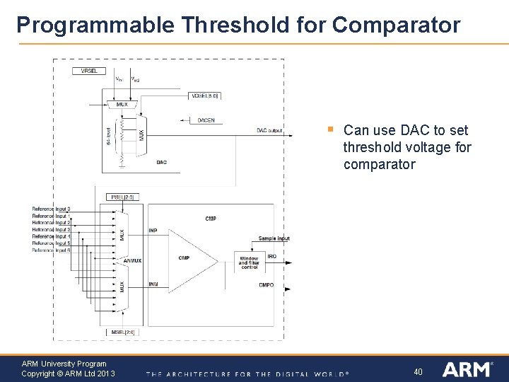
Programmable Threshold for Comparator § ARM University Program Copyright © ARM Ltd 2013 Can use DAC to set threshold voltage for comparator 40

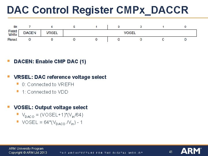
DAC Control Register CMPx_DACCR § DACEN: Enable CMP DAC (1) § VRSEL: DAC reference voltage select § § § 0: Connected to VREFH 1: Connected to VDD VOSEL: Output voltage select § § VDACO = (VOSEL+1)*(Vin/64) VOSEL = 64*(VDACO /Vin) - 1 ARM University Program Copyright © ARM Ltd 2013 41

ANALOG TO DIGITAL CONVERTER ARM University Program Copyright © ARM Ltd 2013 42

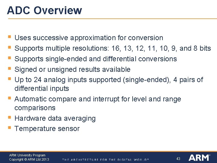
ADC Overview § § § § Uses successive approximation for conversion Supports multiple resolutions: 16, 13, 12, 11, 10, 9, and 8 bits Supports single-ended and differential conversions Signed or unsigned results available Up to 24 analog inputs supported (single-ended), 4 pairs of differential inputs Automatic compare and interrupt for level and range comparisons Hardware data averaging Temperature sensor ARM University Program Copyright © ARM Ltd 2013 43

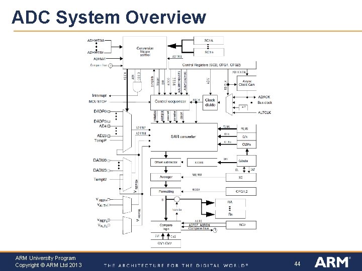
ADC System Overview ARM University Program Copyright © ARM Ltd 2013 44

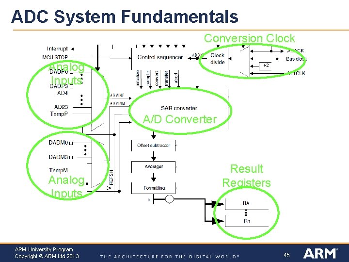
ADC System Fundamentals Conversion Clock Analog Inputs A/D Converter Analog Inputs ARM University Program Copyright © ARM Ltd 2013 Result Registers 45

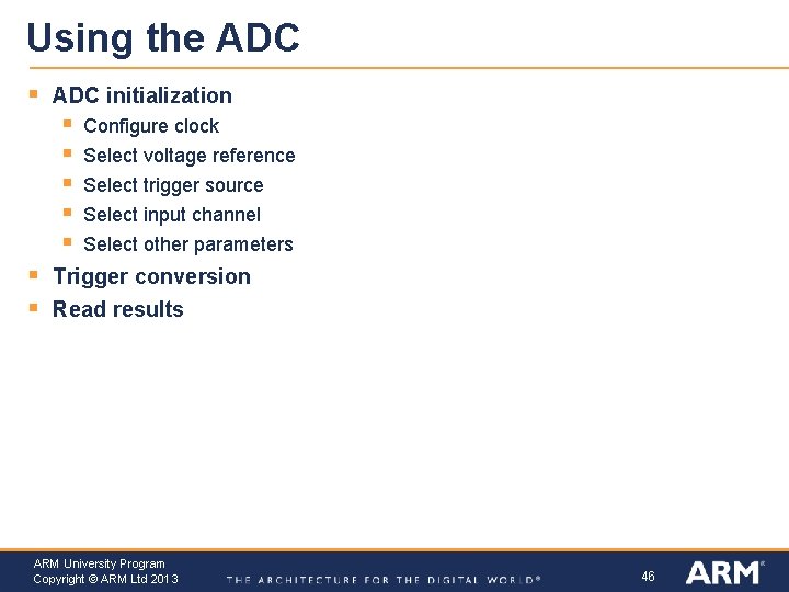
Using the ADC § ADC initialization § § § § Configure clock Select voltage reference Select trigger source Select input channel Select other parameters Trigger conversion Read results ARM University Program Copyright © ARM Ltd 2013 46

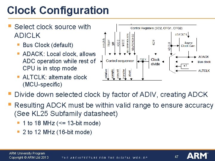
Clock Configuration § Select clock source with ADICLK § § § Bus Clock (default) ADACK: Local clock, allows ADC operation while rest of CPU is in stop mode ALTCLK: alternate clock (MCU-specific) Divide down selected clock by factor of ADIV, creating ADCK Resulting ADCK must be within valid range to ensure accuracy (See KL 25 Subfamily datasheet) § § 1 to 18 MHz (<= 13 -bit mode) 2 to 12 MHz (16 -bit mode) ARM University Program Copyright © ARM Ltd 2013 47

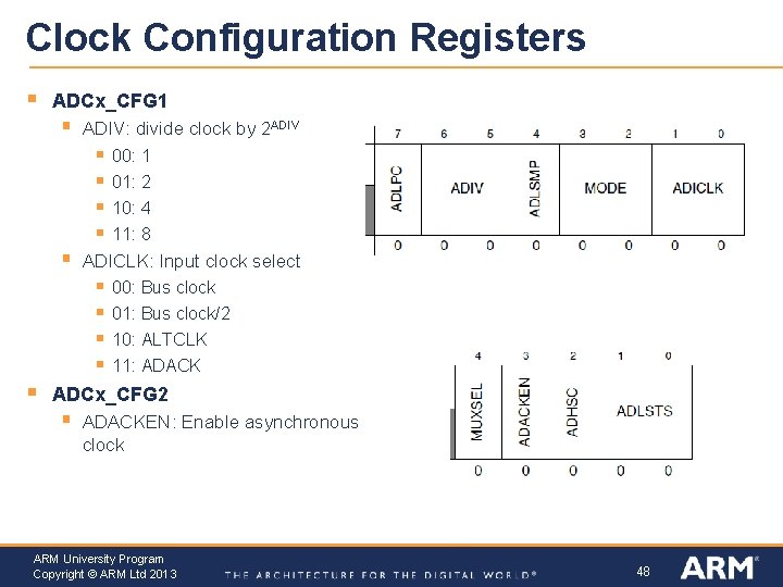
Clock Configuration Registers § ADCx_CFG 1 § ADIV: divide clock by 2 ADIV § § § 01: 2 10: 4 11: 8 ADICLK: Input clock select § § § 00: 1 00: Bus clock 01: Bus clock/2 10: ALTCLK 11: ADACK ADCx_CFG 2 § ADACKEN: Enable asynchronous clock ARM University Program Copyright © ARM Ltd 2013 48

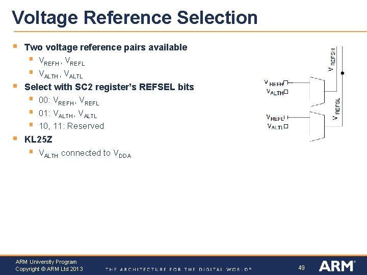
Voltage Reference Selection § Two voltage reference pairs available § § § Select with SC 2 register’s REFSEL bits § § VREFH, VREFL VALTH, VALTL 00: VREFH, VREFL 01: VALTH, VALTL 10, 11: Reserved KL 25 Z § VALTH connected to VDDA ARM University Program Copyright © ARM Ltd 2013 49

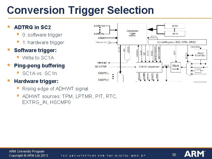
Conversion Trigger Selection § ADTRG in SC 2 § § § Software trigger: § § Write to SC 1 A Ping-pong buffering § § 0: software trigger 1: hardware trigger SC 1 A vs. SC 1 n Hardware trigger: § § Rising edge of ADHWT signal ADHWT sources: TPM, LPTMR, PIT, RTC, EXTRG_IN, HSCMP 0 ARM University Program Copyright © ARM Ltd 2013 50

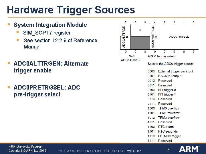
Hardware Trigger Sources § System Integration Module § § SIM_SOPT 7 register See section 12. 2. 6 of Reference Manual § ADC 0 ALTTRGEN: Alternate trigger enable § ADC 0 PRETRGSEL: ADC pre-trigger select ARM University Program Copyright © ARM Ltd 2013 51
![Input Channel Selection Two modes selected by SC 1 nDIFF bit Input Channel Selection § Two modes, selected by SC 1 n[DIFF] bit § §](https://slidetodoc.com/presentation_image/5c72899e83918ed1ad2c9b7a41650aeb/image-52.jpg)
Input Channel Selection § Two modes, selected by SC 1 n[DIFF] bit § § 0: Single-ended 1: Differential § Input channel selected by value of ADCH § Extras § § § Reference voltages Temperature Band Gap ARM University Program Copyright © ARM Ltd 2013 52

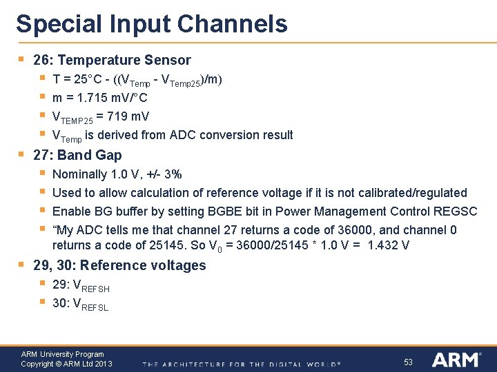
Special Input Channels § 26: Temperature Sensor § § § VTEMP 25 = 719 m. V VTemp is derived from ADC conversion result 27: Band Gap § § § T = 25°C - ((VTemp - VTemp 25)/m) m = 1. 715 m. V/°C Nominally 1. 0 V, +/- 3% Used to allow calculation of reference voltage if it is not calibrated/regulated Enable BG buffer by setting BGBE bit in Power Management Control REGSC “My ADC tells me that channel 27 returns a code of 36000, and channel 0 returns a code of 25145. So V 0 = 36000/25145 * 1. 0 V = 1. 432 V 29, 30: Reference voltages § § 29: VREFSH 30: VREFSL ARM University Program Copyright © ARM Ltd 2013 53

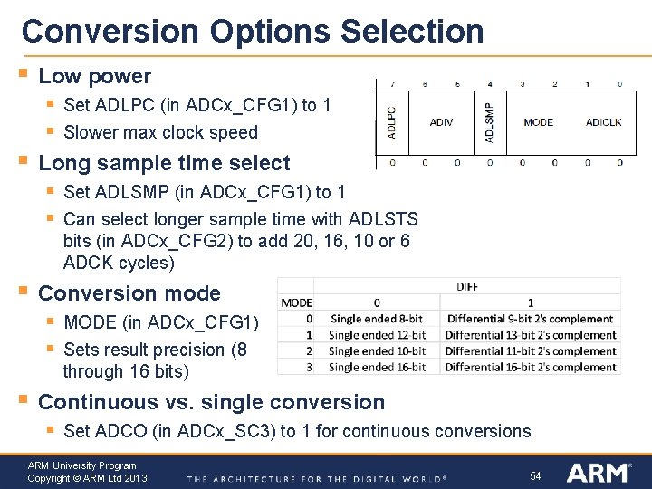
Conversion Options Selection § Low power § § § Set ADLSMP (in ADCx_CFG 1) to 1 Can select longer sample time with ADLSTS bits (in ADCx_CFG 2) to add 20, 16, 10 or 6 ADCK cycles) Conversion mode § § § Slower max clock speed Long sample time select § § § Set ADLPC (in ADCx_CFG 1) to 1 MODE (in ADCx_CFG 1) Sets result precision (8 through 16 bits) Continuous vs. single conversion § Set ADCO (in ADCx_SC 3) to 1 for continuous conversions ARM University Program Copyright © ARM Ltd 2013 54

Conversion Completion § Signaled by COCO bit in SC 1 n § Can generate conversion complete interrupt if AIEN in SC 1 is set § CMSIS-defined ISR name for ADC Interrupt is ADC 0_IRQHandler ARM University Program Copyright © ARM Ltd 2013 55

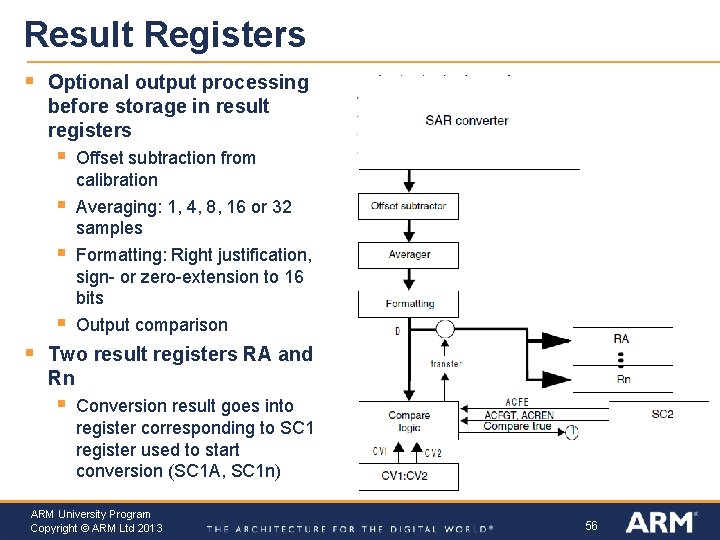
Result Registers § Optional output processing before storage in result registers § § § Offset subtraction from calibration Averaging: 1, 4, 8, 16 or 32 samples Formatting: Right justification, sign- or zero-extension to 16 bits Output comparison Two result registers RA and Rn § Conversion result goes into register corresponding to SC 1 register used to start conversion (SC 1 A, SC 1 n) ARM University Program Copyright © ARM Ltd 2013 56

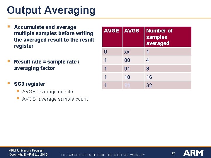
Output Averaging § § § Accumulate and average multiple samples before writing the averaged result to the result register Result rate = sample rate / averaging factor SC 3 register § § AVGE AVGS Number of samples averaged 0 xx 1 1 00 4 1 01 8 1 10 16 1 11 32 AVGE: average enable AVGS: average sample count ARM University Program Copyright © ARM Ltd 2013 57

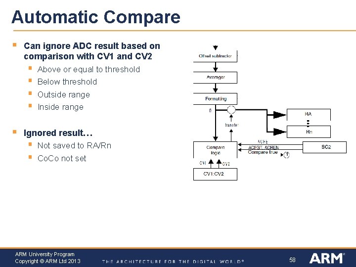
Automatic Compare § Can ignore ADC result based on comparison with CV 1 and CV 2 § § § Above or equal to threshold Below threshold Outside range Inside range Ignored result… § § Not saved to RA/Rn Co. Co not set ARM University Program Copyright © ARM Ltd 2013 58

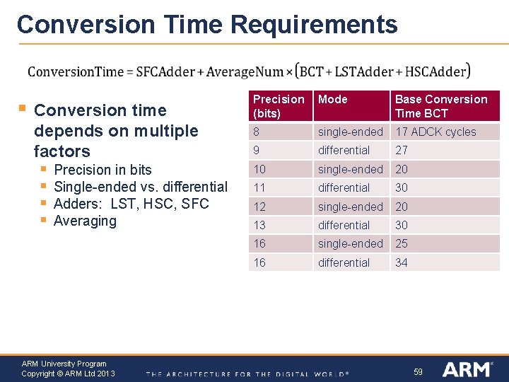
Conversion Time Requirements § Conversion time depends on multiple factors § § Precision in bits Single-ended vs. differential Adders: LST, HSC, SFC Averaging ARM University Program Copyright © ARM Ltd 2013 Precision (bits) Mode Base Conversion Time BCT 8 single-ended 17 ADCK cycles 9 differential 27 10 single-ended 20 11 differential 30 12 single-ended 20 13 differential 30 16 single-ended 25 16 differential 34 59

Using ADC Values § § The ADC gives an integer representing the input voltage relative to the reference voltages Several conversions may be needed § § § Vin = … For some sensor-based applications you will need to compute the physical parameter value based on that voltage (e. g. pressure) – this depends on the sensor’s transfer function You will likely need to do additional computations based on this physical parameter (e. g. compute depth based on pressure) Data type § § § For many applications you will need to compute the approximate input voltage It’s likely that doing these conversions with integer math will lead to excessive loss of precision, so use floating point math AFTER you have the application working, you can think about accelerating the program using fixed-point math (scaled integers). Sometimes you will want to output ASCII characters (to the LCD, for example). You will need to convert the floating point number to ASCII using sprintf, ftoa, or another method. ARM University Program Copyright © ARM Ltd 2013 60