
ANALOG ELECTRONIC CIRCUITS 1 EKT 204 Frequency Response
- Slides: 22
ANALOG ELECTRONIC CIRCUITS 1 EKT 204 Frequency Response of BJT Amplifiers (Part 2) 1
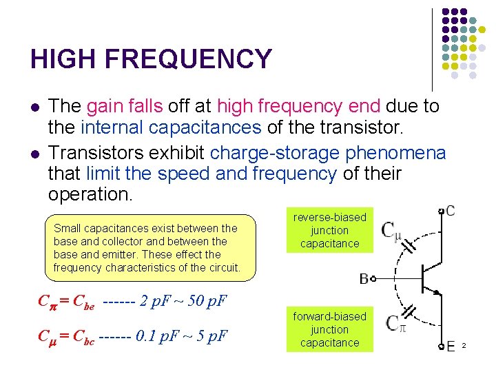
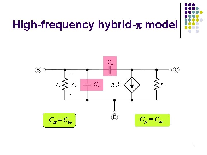
HIGH FREQUENCY l l The gain falls off at high frequency end due to the internal capacitances of the transistor. Transistors exhibit charge-storage phenomena that limit the speed and frequency of their operation. Small capacitances exist between the base and collector and between the base and emitter. These effect the frequency characteristics of the circuit. C = Cbe ------ 2 p. F ~ 50 p. F C = Cbc ------ 0. 1 p. F ~ 5 p. F reverse-biased junction capacitance forward-biased junction capacitance 2
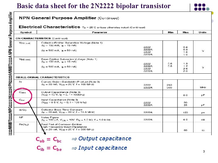
Basic data sheet for the 2 N 2222 bipolar transistor Cob = Cbc Output capacitance Cib = Cbe Input capacitance 3
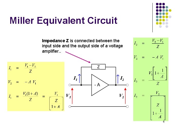
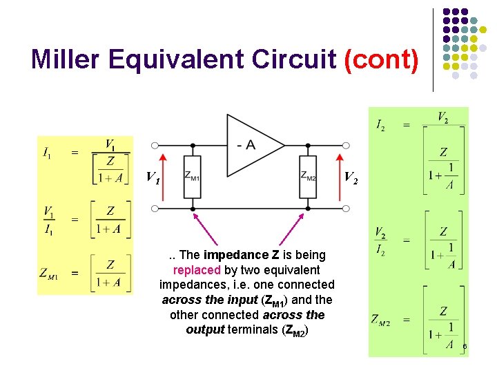
Miller’s Theorem l l This theorem simplifies the analysis of feedback amplifiers. The theorem states that if an impedance is connected between the input side and the output side of a voltage amplifier, this impedance can be replaced by two equivalent impedances, i. e. one connected across the input and the other connected across the output terminals. 4
Miller Equivalent Circuit Impedance Z is connected between the input side and the output side of a voltage amplifier. . I 1 V 1 I 2 V 2 5
Miller Equivalent Circuit (cont) V 1 V 2 . . The impedance Z is being replaced by two equivalent impedances, i. e. one connected across the input (ZM 1) and the other connected across the output terminals (ZM 2) 6
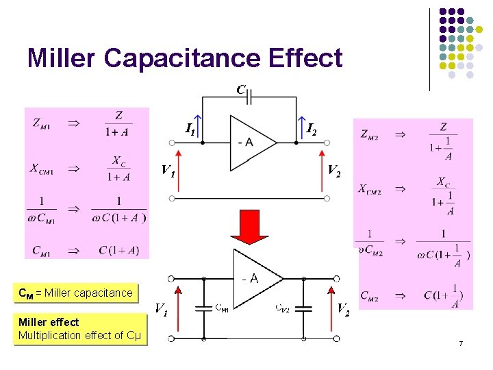
Miller Capacitance Effect C I 1 V 1 I 2 V 2 CM = Miller capacitance Miller effect Multiplication effect of Cµ 7
High-frequency hybrid- model C + r V C gm. V ro - C = Cbe C = Cbc 8
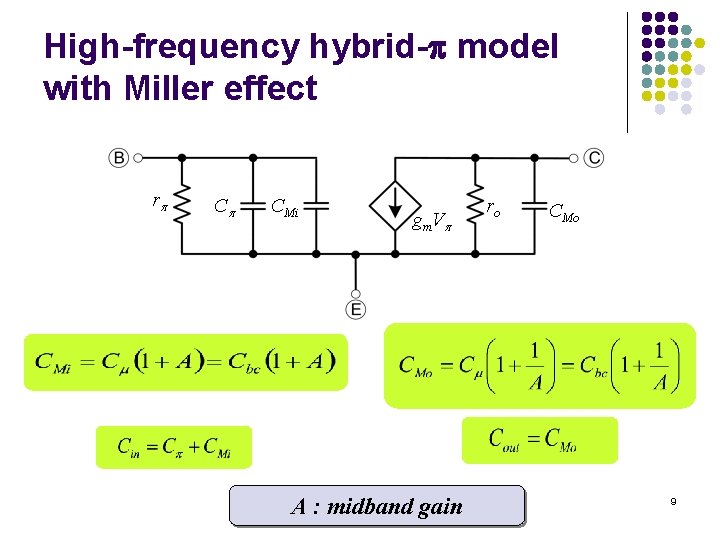
High-frequency hybrid- model with Miller effect r C CMi gm. V A : midband gain ro CMo 9
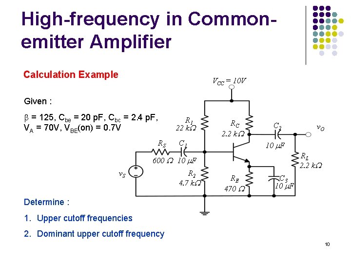
High-frequency in Commonemitter Amplifier Calculation Example VCC = 10 V Given : = 125, Cbe = 20 p. F, Cbc = 2. 4 p. F, VA = 70 V, VBE(on) = 0. 7 V RS R 1 22 k RC 2. 2 k C 1 C 2 10 F RL 2. 2 k 600 10 F v. S R 2 4. 7 k v. O RE 470 C 3 10 F Determine : 1. Upper cutoff frequencies 2. Dominant upper cutoff frequency 10
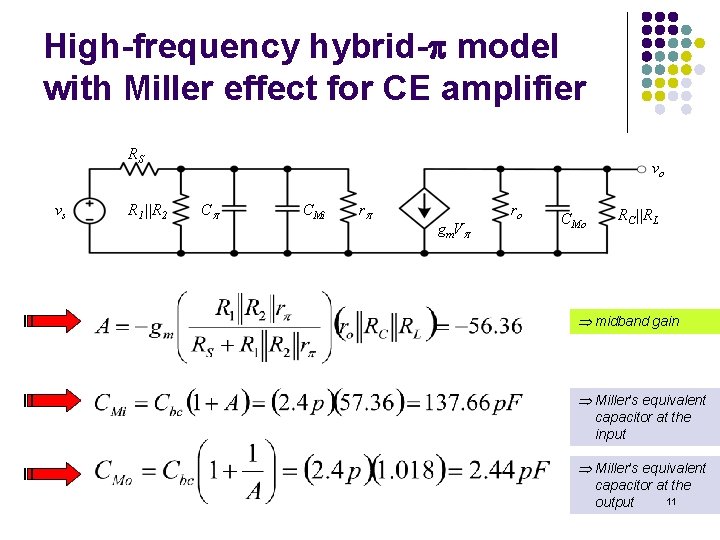
High-frequency hybrid- model with Miller effect for CE amplifier RS vs R 1||R 2 vo C CMi r gm. V ro CMo RC||RL midband gain Miller’s equivalent capacitor at the input Miller’s equivalent capacitor at the 11 output
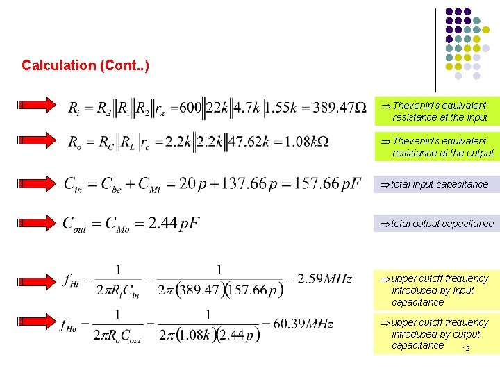
Calculation (Cont. . ) Thevenin’s equivalent resistance at the input Thevenin’s equivalent resistance at the output total input capacitance total output capacitance upper cutoff frequency introduced by input capacitance upper cutoff frequency introduced by output capacitance 12
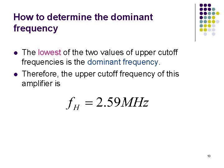
How to determine the dominant frequency l l The lowest of the two values of upper cutoff frequencies is the dominant frequency. Therefore, the upper cutoff frequency of this amplifier is 13
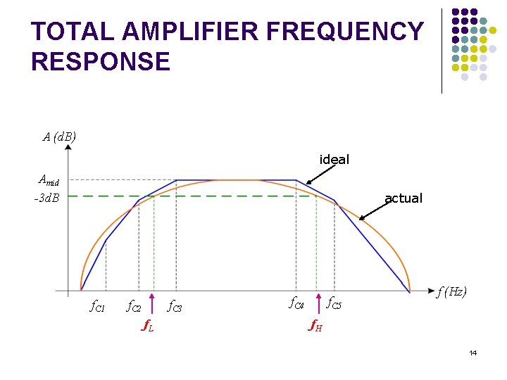
TOTAL AMPLIFIER FREQUENCY RESPONSE A (d. B) ideal Amid actual -3 d. B f. C 1 f. C 2 f. C 3 f. L f. C 4 f. C 5 f (Hz) f. H 14
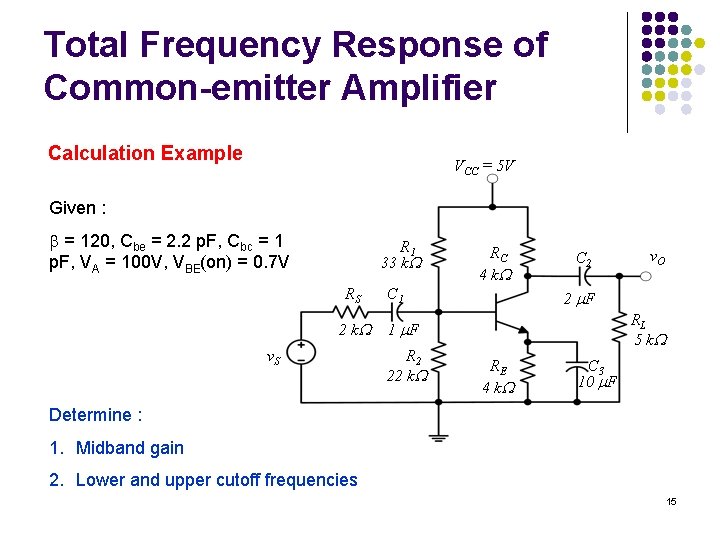
Total Frequency Response of Common-emitter Amplifier Calculation Example VCC = 5 V Given : = 120, Cbe = 2. 2 p. F, Cbc = 1 p. F, VA = 100 V, VBE(on) = 0. 7 V R 1 33 k RS 2 k v. S RC 4 k C 1 C 2 2 F RL 5 k 1 F R 2 22 k v. O RE 4 k C 3 10 F Determine : 1. Midband gain 2. Lower and upper cutoff frequencies 15
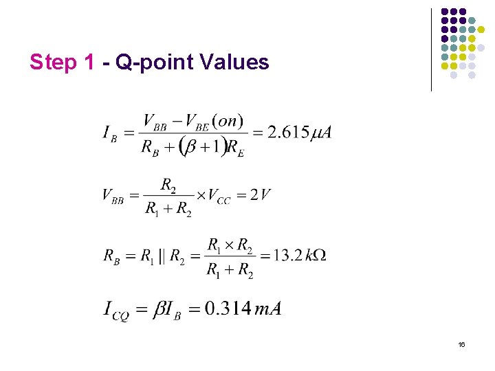
Step 1 - Q-point Values 16
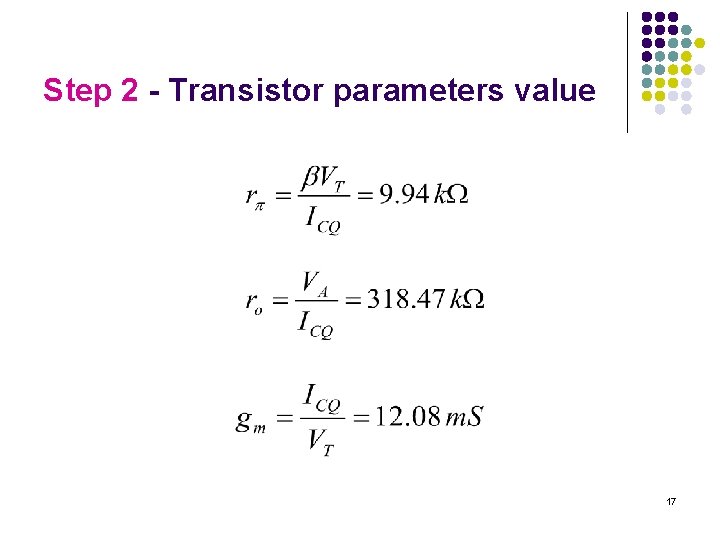
Step 2 - Transistor parameters value 17
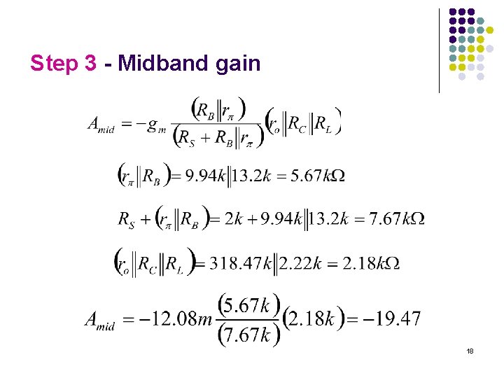
Step 3 - Midband gain 18
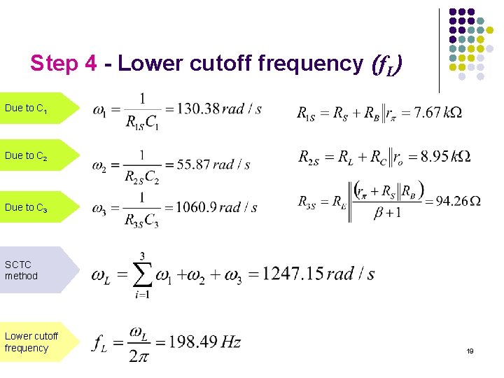
Step 4 - Lower cutoff frequency (f. L) Due to C 1 Due to C 2 Due to C 3 SCTC method Lower cutoff frequency 19
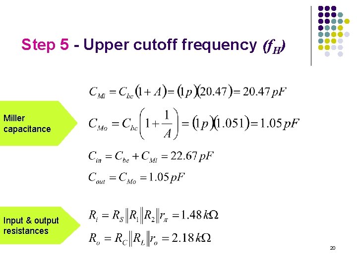
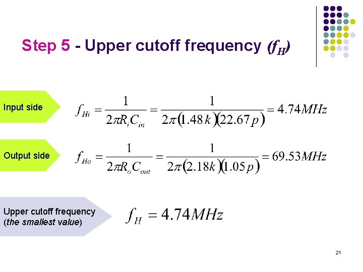
Step 5 - Upper cutoff frequency (f. H) Miller capacitance Input & output resistances 20
Step 5 - Upper cutoff frequency (f. H) Input side Output side Upper cutoff frequency (the smallest value) 21
Exercise Textbook: Donald A. Neamen, ‘MICROELECTRONICS Circuit Analysis & Design’, 3 rd Edition’, Mc. Graw Hill International Edition, 2007 q Exercise 7. 11 q 22