An Overview of IQ Modulation and Demodulation Techniques
- Slides: 10

An Overview of IQ Modulation and Demodulation Techniques for Cavity LLRF Control CI Lecture Series Summer 2010

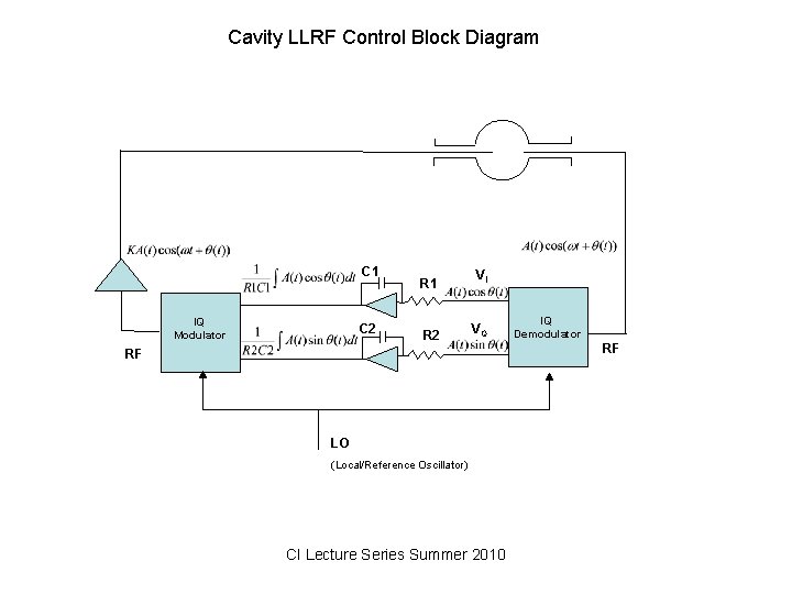
Cavity LLRF Control Block Diagram C 1 IQ Modulator C 2 R 1 R 2 VI VQ RF LO (Local/Reference Oscillator) CI Lecture Series Summer 2010 IQ Demodulator RF

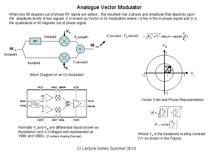
Analogue Vector Modulator When two 90 degrees out of phase RF signal are added , the resultant has a phase and amplitude that depends upon the amplitude levels of two signals. It is known as Vector or IQ modulation where I is the in-phase signal and Q is the quadrature or 90 degrees out of phase signal. VQ 90 o RFout RFin VQ 1 A VI өQ Block Diagram of an IQ modulator -1 I 1 VI -1 Vector Gain and Phase Representation Normally VI and VQ are differential Inputs known as Baseband I and Q Voltages and represented as VBBI and VBBQ. (Courtesy Analog Devices) CI Lecture Series Summer 2010 Where Vo is the baseband scaling constant (1 V as shown in the Figure).

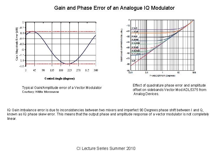
Gain and Phase Error of an Analogue IQ Modulator Control Angle (degrees) Typical Gain/Amplitude error of a Vector Modulator Courtesy: Hittite Microwaves Effect of quadrature phase error and amplitude offset on sidebands Vector Mod ADL 5375 from Analog Devices. IQ Gain imbalance error is due to inconsistencies between two mixers and imperfect 90 Degrees phase shift between I and Q, known as IQ phase skew error. This means that the output phase and amplitude response of a vector modulator is not completely linear. CI Lecture Series Summer 2010

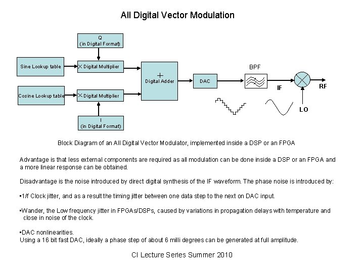
All Digital Vector Modulation Q (in Digital Format) Sine Lookup table BPF Digital Multiplier Digital Adder DAC RF IF Cosine Lookup table Digital Multiplier LO I (in Digital Format) Block Diagram of an All Digital Vector Modulator, implemented inside a DSP or an FPGA Advantage is that less external components are required as all modulation can be done inside a DSP or an FPGA and a more linear response can be obtained. Disadvantage is the noise introduced by direct digital synthesis of the IF waveform. The phase noise is introduced by: • 1/f Clock jitter, and as a result the timing jitter between one data step to the next on DAC input. • Wander, the Low frequency jitter in FPGAs/DSPs, caused by variations in propagation delays with temperature and close in noise of the clock. • DAC nonlinearities. Using a 16 bit fast DAC, ideally a phase step of about 6 milli degrees can be generated at full amplitude. CI Lecture Series Summer 2010

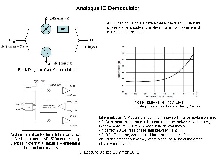
Analogue IQ Demodulator VQ An IQ demodulator is a device that extracts an RF signal’s phase and amplitude information in terms of in-phase and quadrature components. 90 o LOin RFin VI Block Diagram of an IQ demodulator Noise Figure vs RF Input Level Courtesy: Device datasheet from Analog Devices Architecture of an IQ demodulator as shown In Device datasheet ADL 5380 from Analog Devices. Note that all Inputs are differential in order to keep the noise low. Like analogue IQ Modulators, common issues with IQ Demodulators are; • IQ Gain imbalance error due to inconsistencies between two mixers, is of the order of +/-0. 2 db in modern IQ demodulators. • Imperfect 90 Degrees phase shift between I and Q. • IQ DC offset error, which is residual error and I and Q outputs, and of the order of a few m. V, where signal could be of the order of a few micro volts. CI Lecture Series Summer 2010

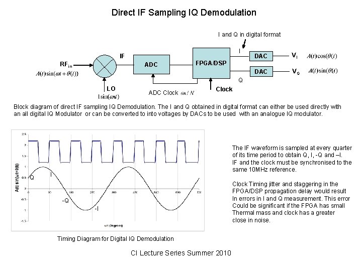
Direct IF Sampling IQ Demodulation I and Q in digital format I IF RFin ADC DAC VI DAC VQ FPGA/DSP Q LO ADC Clock Block diagram of direct IF sampling IQ Demodulation. The I and Q obtained in digital format can either be used directly with an all digital IQ Modulator or can be converted to into voltages by DACs to be used with an analogue IQ modulator. Q The IF waveform is sampled at every quarter of its time period to obtain Q, I, -Q and –I. IF and the clock must be synchronised to the same 10 MHz reference. I Clock Timing jitter and staggering in the FPGA/DSP propagation delay would result In errors in I and Q measurement. This error Could be significant if the FPGA has small Thermal mass and clock has a greater close in noise. -Q -I Timing Diagram for Digital IQ Demodulation CI Lecture Series Summer 2010

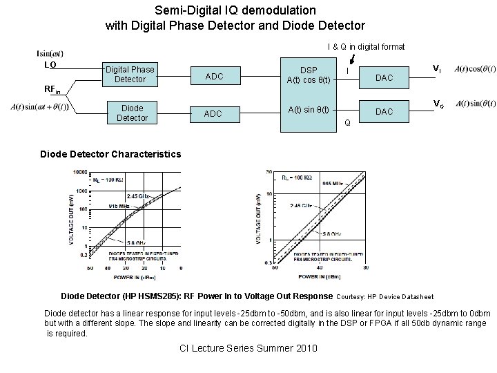
Semi-Digital IQ demodulation with Digital Phase Detector and Diode Detector I & Q in digital format LO Digital Phase Detector ADC RFin Diode Detector ADC DSP A(t) cos θ(t) I A(t) sin θ(t) DAC VI VQ Q Diode Detector Characteristics Diode Detector (HP HSMS 285): RF Power In to Voltage Out Response Courtesy: HP Device Datasheet Diode detector has a linear response for input levels -25 dbm to -50 dbm, and is also linear for input levels -25 dbm to 0 dbm but with a different slope. The slope and linearity can be corrected digitally in the DSP or FPGA if all 50 db dynamic range is required. CI Lecture Series Summer 2010

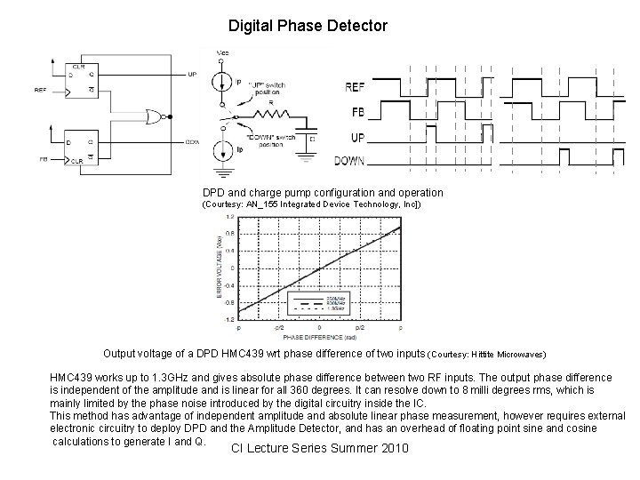
Digital Phase Detector DPD and charge pump configuration and operation (Courtesy: AN_155 Integrated Device Technology, Inc]) Output voltage of a DPD HMC 439 wrt phase difference of two inputs (Courtesy: Hittite Microwaves) HMC 439 works up to 1. 3 GHz and gives absolute phase difference between two RF inputs. The output phase difference is independent of the amplitude and is linear for all 360 degrees. It can resolve down to 8 milli degrees rms, which is mainly limited by the phase noise introduced by the digital circuitry inside the IC. This method has advantage of independent amplitude and absolute linear phase measurement, however requires external electronic circuitry to deploy DPD and the Amplitude Detector, and has an overhead of floating point sine and cosine calculations to generate I and Q. CI Lecture Series Summer 2010

All different techniques of IQ modulation and demodulation mentioned above have their own advantages and disadvantages in terms of linearity, noise and ease of implementation. What method is best suited for a low level RF control, would depend upon the requirements of a particular application, CI Lecture Series Summer 2010