An Oscillating Active CMOS Pixel for Subretinal Stimulation

An Oscillating Active CMOS Pixel for Subretinal Stimulation D. Ziegler, S. Ferazzutti, D. Bertrand, A. M. Ionescu and Ph. Renaud EPFL Microsystems Laboratory (Lausanne, Switzerland) Published at Eurosensors XVI DMS Group Meeting: October 18, 2002
An Oscillating Active CMOS Pixel for Subretinal Stimulation • This article presents a photodiode circuit whose output is intended to simulate the input necessary to replace biological photoreceptors in stimulating the first-stage processing circuitry in the retina. • The circuits are intended to be powered remotely, via RF control, and to become a true “replacement” for failed photoreceptors in the human retina
An Oscillating Active CMOS Pixel for Subretinal Stimulation • Pieces of the Puzzle – Photoreceptor = PIN photodiode fabricated in a standard 0. 35 micron CMOS process • sensitivie between 1 m. W/cm 2 to 10 m. W/cm 2 – Oscillator circuitry = converts light intensity to a pulse stream, whose frequency is proportional to intensity • frequencies between 4 and 400 Hz (low to high intensity) – RF interface = remote powering of photoreceptors, oscillator circuits and other support circuitry. – Single pixel (75 X 75 mm 2 and 100 X 100 mm 2) results presented in this work.
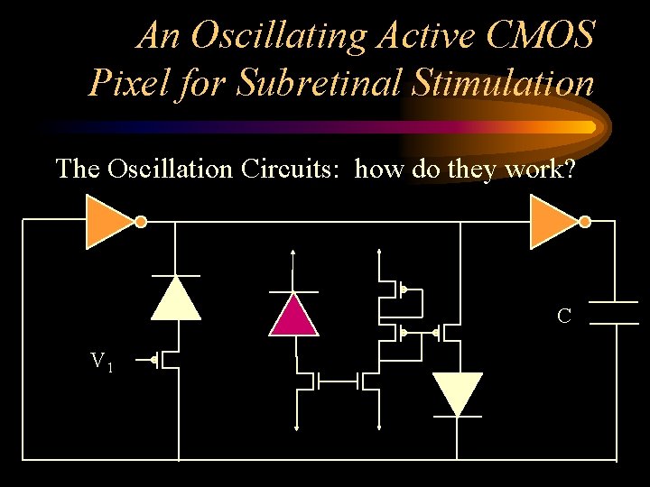
An Oscillating Active CMOS Pixel for Subretinal Stimulation The Oscillation Circuits: how do they work? C V 1
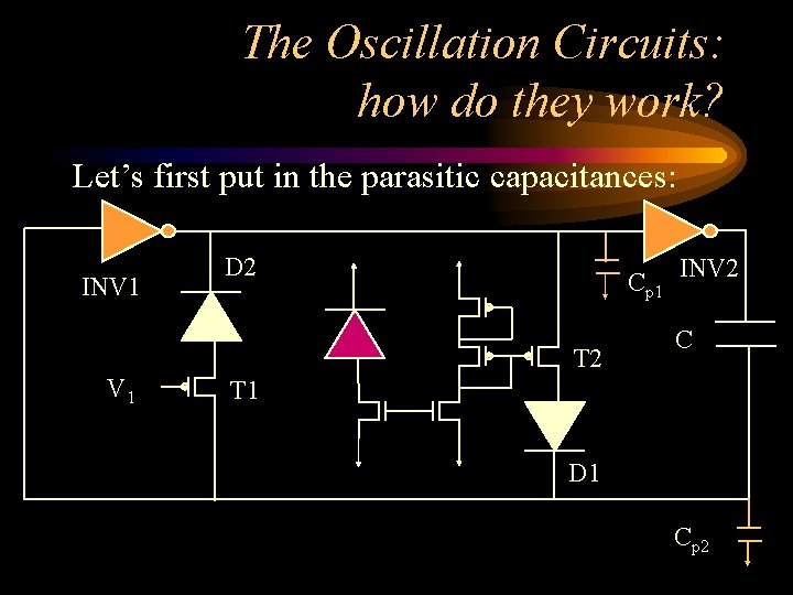
The Oscillation Circuits: how do they work? Let’s first put in the parasitic capacitances: INV 1 D 2 Cp 1 T 2 V 1 INV 2 C T 1 D 1 Cp 2
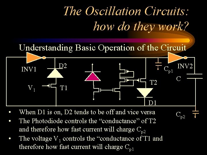
The Oscillation Circuits: how do they work? Understanding Basic Operation of the Circuit INV 1 • • • D 2 T 1 T 2 D 1 When D 1 is on, D 2 tends to be off and vice versa The Photodiode controls the “conductance” of T 2 and therefore how fast current will charge Cp 2 The voltage V 1 controls the “conductance of T 1 and therefore how fast current will charge Cp 1 INV 2 C Cp 2
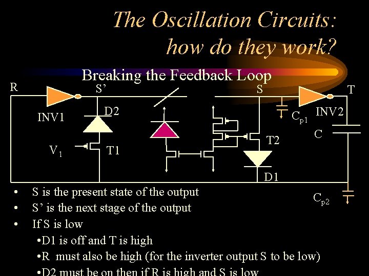
The Oscillation Circuits: how do they work? Breaking the Feedback Loop R S’ INV 1 S D 2 T 1 T 2 T Cp 1 INV 2 C D 1 • • • S is the present state of the output Cp 2 S’ is the next stage of the output If S is low • D 1 is off and T is high • R must also be high (for the inverter output S to be low)
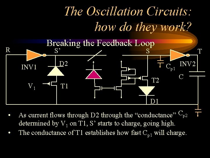
The Oscillation Circuits: how do they work? Breaking the Feedback Loop R S’ INV 1 S D 2 T 1 T 2 T Cp 1 INV 2 C D 1 • • As current flows through D 2 through the “conductance” Cp 2 determined by V 1 on T 1, S’ starts to charge, going high. The conductance of T 1 establishes how fast Cp 1 will charge.

The Oscillation Circuits: how do they work? Breaking the Feedback Loop R S’ INV 1 S D 2 T 1 T 2 T Cp 1 INV 2 C D 1 • If S is high Cp 2 • D 1 is on and T is low • R must also be low (for the inverter output S to be high) • D 2 must be off then if R is low and S is high
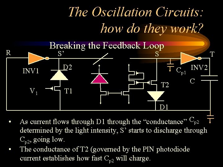
The Oscillation Circuits: how do they work? Breaking the Feedback Loop R S’ INV 1 S D 2 T 1 T 2 T Cp 1 INV 2 C D 1 • • As current flows through D 1 through the “conductance” Cp 2 determined by the light intensity, S’ starts to discharge through Cp 2, going low. The conductance of T 2 (governed by the PIN photodiode current establishes how fast Cp 2 will charge.
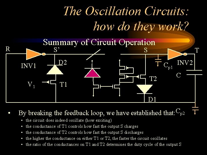
The Oscillation Circuits: how do they work? Summary of Circuit Operation R S’ INV 1 S D 2 T 1 T 2 T Cp 1 INV 2 C D 1 • By breaking the feedback loop, we have established that: Cp 2 • • • the circuit does indeed oscillate (how exciting) the conductance of T 1 controls how fast the output S charges the conductance of T 2 controls how fast the output S discharges the higher the conductance on either T 1 or T 2, the faster the circuit oscillates the ratio of the conductances on T 1 and T 2 determines the duty cycle of the output S
An Oscillating Active CMOS Pixel for Subretinal Stimulation • Issues with the Oscillator Circuit – It is very noisy at low light intesn ities (less than 0. 5 X 10 -5 W/cm 2. – The duty cycle changes with frequency – Parasitic light limits the minimum duty cycle – Oscillations stop at high light intensities – Other Issues or Advantages to this circuit?
- Slides: 12