An Introduction to Matching and Layout Alan Hastings

- Slides: 21

An Introduction to Matching and Layout Alan Hastings Texas Instruments 1

Overview of Matching u Two devices with the same physical layout never have quite the same electrical properties. n n n Variations between devices are called mismatches. Mismatches may have large impacts on certain circuit parameters, for example common mode rejection ratio (CMRR). By default, simulators such as SPICE do not model mismatches. The designer must deliberately insert mismatches to see their effects. 2

Kinds of Mismatch u Mismatches may be either random or systematic, or a combination of both. n n n Suppose two matched devices have parameters P 1 and P 2. Then let the mismatch between the devices equal P = P 2 – P 1. For a sample of units, measure P. Compute sample mean m( P ) and standard deviation s( P ). m( P ) is a measure of systematic mismatch. s( P) is a measure of random mismatch. 3

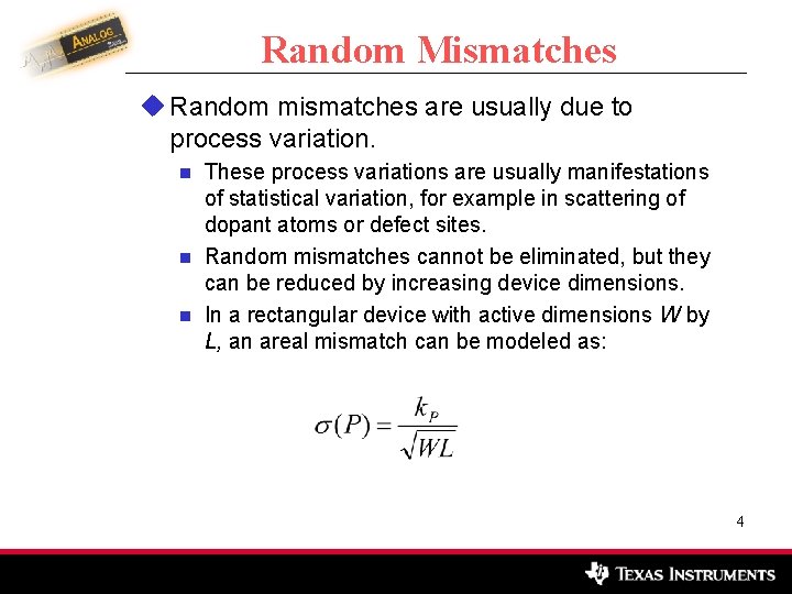
Random Mismatches u Random mismatches are usually due to process variation. n n n These process variations are usually manifestations of statistical variation, for example in scattering of dopant atoms or defect sites. Random mismatches cannot be eliminated, but they can be reduced by increasing device dimensions. In a rectangular device with active dimensions W by L, an areal mismatch can be modeled as: 4

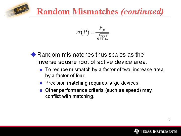
Random Mismatches (continued) u Random mismatches thus scales as the inverse square root of active device area. n n n To reduce mismatch by a factor of two, increase area by a factor of four. Precision matching requires large devices. Other performance criteria (such as speed) may conflict with matching. 5

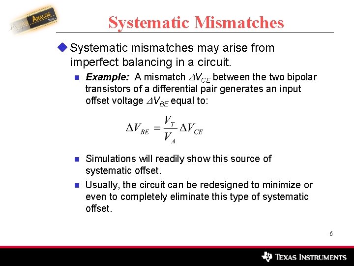
Systematic Mismatches u Systematic mismatches may arise from imperfect balancing in a circuit. n Example: A mismatch VCE between the two bipolar transistors of a differential pair generates an input offset voltage VBE equal to: n Simulations will readily show this source of systematic offset. Usually, the circuit can be redesigned to minimize or even to completely eliminate this type of systematic offset. n 6

Gradients u Systematic mismatches may also arise from gradients. n Certain physical parameters may vary gradually across an integrated circuit, for example: w Temperature w Pressure w Oxide thickness n n These types of variations are usually treated as 2 D fields, the gradients of which can (at least theoretically) be computed or measured. Because of the way we mathematically treat these variations, they are called gradients. 7

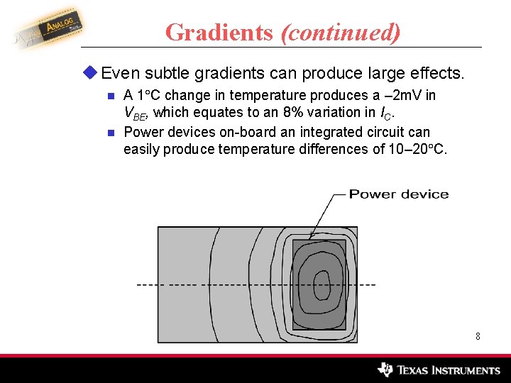
Gradients (continued) u Even subtle gradients can produce large effects. n n A 1 C change in temperature produces a – 2 m. V in VBE, which equates to an 8% variation in IC. Power devices on-board an integrated circuit can easily produce temperature differences of 10– 20 C. 8

Analyzing Gradients u For a simplified analysis of gradients: n Make the following assumptions of linearity: w The gradient is constant over the area of interest. w Electrical parameters depend linearly upon physical parameters. n Although neither assumption is strictly true, they are usually approximately true, at least for properly laid out devices. 9

Analyzing Gradients (continued) u Assuming linearity, n n n We can reduce each distributed device to a lumped device located at the centroid of the device area. The magnitude of the mismatch equals the product of the distance between the centroids and the magnitude of the gradient along the axis of separation. Therefore we can reduce the impact of the mismatch by reducing the separation of the centroids. 10

How to Find a Centroid (Easily) u Rules for finding a centroid (assuming linearity): n n If a geometric figure has an axis of symmetry, then the centroid lies on it. If a geometric figure has two or more axes of symmetry, then the centroid must lie at their intersection. 11

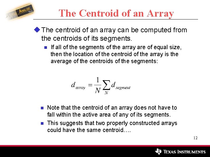
The Centroid of an Array u The centroid of an array can be computed from the centroids of its segments. n n n If all of the segments of the array are of equal size, then the location of the centroid of the array is the average of the centroids of the segments: Note that the centroid of an array does not have to fall within the active area of any of its segments. This suggests that two properly constructed arrays could have the same centroid…. 12

Common-centroid Arrays u Arrays whose centroids coincide are called common-centroid arrays. n n Theoretically, a common-centroid array should entirely cancel systematic mismatches due to gradients. In practice, this doesn’t happen because the assumptions of linearity are only approximately true. Common-centroids don’t help random mismatches at all. Neither are they a cure for sloppy circuit design! Virtually all precisely matched components in integrated circuits use common centroids. 13

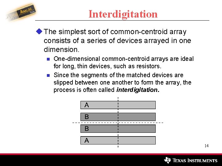
Interdigitation u The simplest sort of common-centroid array consists of a series of devices arrayed in one dimension. n n One-dimensional common-centroid arrays are ideal for long, thin devices, such as resistors. Since the segments of the matched devices are slipped between one another to form the array, the process is often called interdigitation. 14

Interdigitation (continued) u Not all interdigitated arrays are made equal! n n Certain arrays precisely align the centroids of the matched devices (A, C). These provide superior matching. Other arrays only approximately align the centroids (B). These provide inferior matching. 15

2 D Cross-coupled Arrays u A more elaborate sort of common-centroid array involves devices cross-coupled in a rectangular two-dimensional array. n This type of array is ideal for roughly square devices, such as capacitors and bipolars. 16

2 D Cross-coupled Arrays (cont’d) u The simplest two-dimensional cross-coupled array contains four segments. n n n This type of array is called a cross-coupled pair. For many devices, particularly smaller ones, the cross-coupled pair provides the best possible layout. More complicated 2 D arrays containing more segments provide better matching for large devices because they minimize the impact of nonlinearities. 17

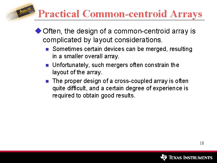
Practical Common-centroid Arrays u Often, the design of a common-centroid array is complicated by layout considerations. n n n Sometimes certain devices can be merged, resulting in a smaller overall array. Unfortunately, such mergers often constrain the layout of the array. The proper design of a cross-coupled array is often quite difficult, and a certain degree of experience is required to obtain good results. 18

2: 1: 2 Bipolar Array u This array matches a 4 X and a 1 X bipolar transistor using interdigitation. 19

4: 1: 4 Bipolar Array u This array matches an 8 X and a 1 X bipolar transistor using interdigitation. 20

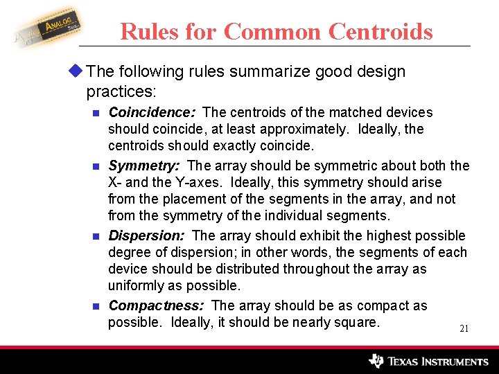
Rules for Common Centroids u The following rules summarize good design practices: n n Coincidence: The centroids of the matched devices should coincide, at least approximately. Ideally, the centroids should exactly coincide. Symmetry: The array should be symmetric about both the X- and the Y-axes. Ideally, this symmetry should arise from the placement of the segments in the array, and not from the symmetry of the individual segments. Dispersion: The array should exhibit the highest possible degree of dispersion; in other words, the segments of each device should be distributed throughout the array as uniformly as possible. Compactness: The array should be as compact as possible. Ideally, it should be nearly square. 21