An Introduction to FPGA and SOPC Development Board
An Introduction to FPGA and SOPC Development Board Yong Wang
Outline • • • What are Programmable Logic Devices? Architecture and Examples Why FPGA? Vendors and Devices Development on Altera Device Summary
Programmable Logic Devices • Programmable digital integrated circuit • Desired functionality is implemented by configuring on-chip logic blocks and interconnections • Developers only care about the logic design but not the internal hard-wire connection ( softwarelize the hardware design)
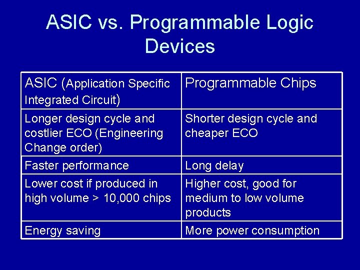
ASIC vs. Programmable Logic Devices ASIC (Application Specific Integrated Circuit) Programmable Chips Longer design cycle and costlier ECO (Engineering Change order) Faster performance Lower cost if produced in high volume > 10, 000 chips Shorter design cycle and cheaper ECO Energy saving More power consumption Long delay Higher cost, good for medium to low volume products
Type of Programmable Logic Devices • PLA (Programmable Logic Array) • CPLD (Complex Programmable Logic Device) • FPGA (Field Programmable Gate Array)
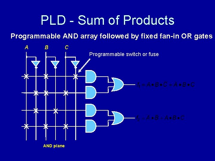
PLD - Sum of Products Programmable AND array followed by fixed fan-in OR gates A B C Programmable switch or fuse AND plane
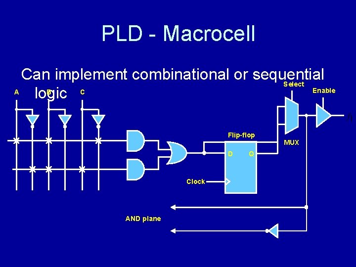
PLD - Macrocell Can implement combinational or sequential Select Enable B A C logic Flip-flop MUX D Clock AND plane Q
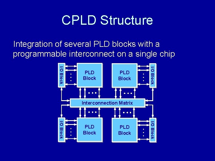
CPLD Structure Integration of several PLD blocks with a programmable interconnect on a single chip PLD Block • • • I/O Block PLD Block I/O Block • • • Interconnection Matrix I/O Block • • • PLD Block
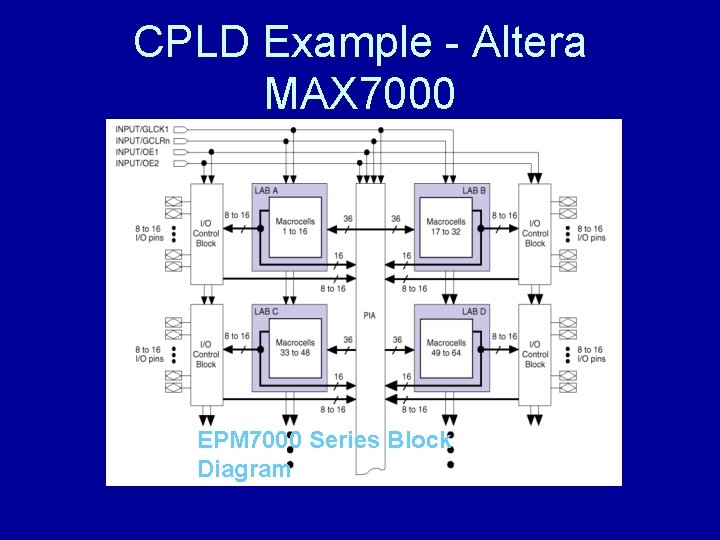
CPLD Example - Altera MAX 7000 EPM 7000 Series Block Diagram
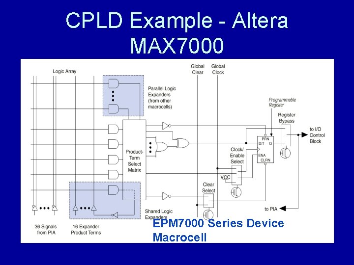
CPLD Example - Altera MAX 7000 EPM 7000 Series Device Macrocell
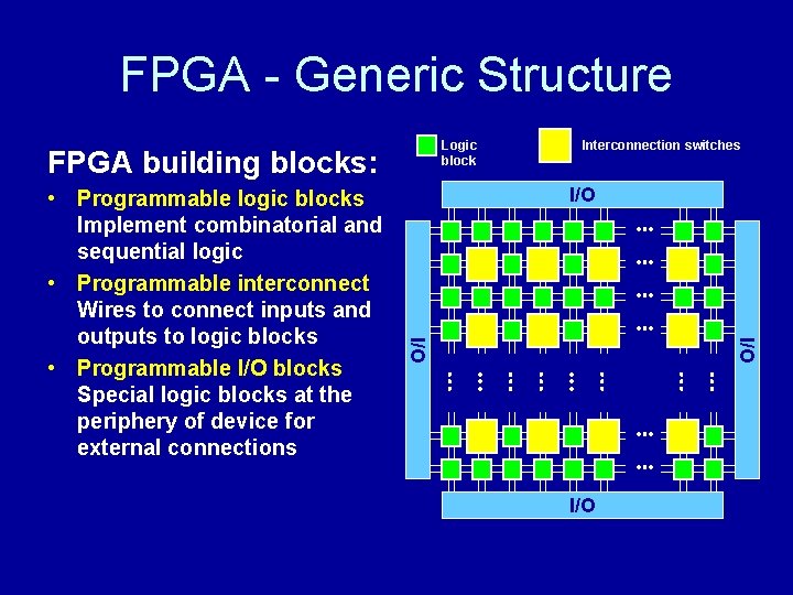
FPGA - Generic Structure Logic block FPGA building blocks: I/O I/O • Programmable logic blocks Implement combinatorial and sequential logic • Programmable interconnect Wires to connect inputs and outputs to logic blocks • Programmable I/O blocks Special logic blocks at the periphery of device for external connections Interconnection switches I/O
Other FPGA Building Blocks • Clock distribution • Embedded memory blocks • Special purpose blocks: – DSP blocks: • Hardware multipliers, adders and registers – Embedded microprocessors/microcontrollers – High-speed serial transceivers
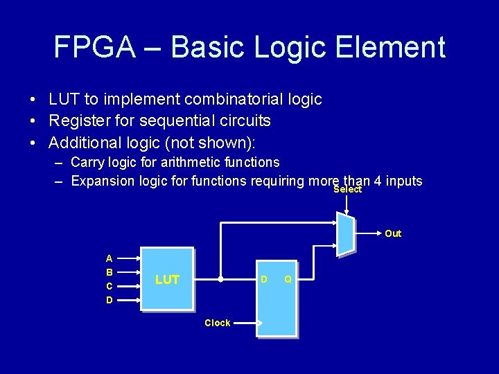
FPGA – Basic Logic Element • LUT to implement combinatorial logic • Register for sequential circuits • Additional logic (not shown): – Carry logic for arithmetic functions – Expansion logic for functions requiring more than 4 inputs Select Out A B C D LUT D Clock Q
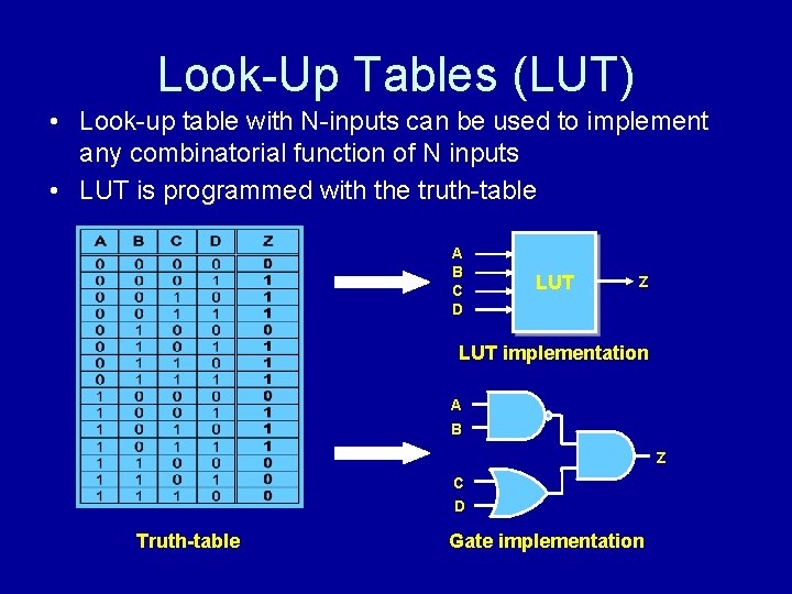
Look-Up Tables (LUT) • Look-up table with N-inputs can be used to implement any combinatorial function of N inputs • LUT is programmed with the truth-table A B C D LUT Z LUT implementation A B Z C D Truth-table Gate implementation
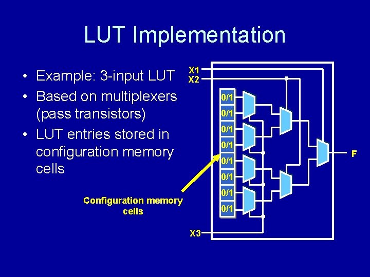
LUT Implementation • Example: 3 -input LUT • Based on multiplexers (pass transistors) • LUT entries stored in configuration memory cells X 1 X 2 0/1 0/1 Configuration memory cells 0/1 X 3 F
Other FPGA Building Blocks • Clock distribution • Embedded memory blocks • Special purpose blocks: – DSP blocks: • Hardware multipliers, adders and registers – Embedded microprocessors/microcontrollers – High-speed serial transceivers
Special Features • Clock management – PLL, DLL – Eliminate clock skew between external clock input and on-chip clock – Low-skew global clock distribution network • • Support for various interface standards High-speed serial I/Os Embedded processor cores DSP blocks
Configuration Storage Elements • Static Random Access Memory (SRAM) – Logical configuration is controlled by the state of SRAM bits – FPGA needs to be configured at power-on by another separated ROM • Flash Erasable Programmable ROM (Flash) – – Logical configuration is implemented by floatinggate transistors that can be turned off by injecting charge onto its gate. FPGA itself holds the program – reprogrammable, even in-circuit
Example: Altera Stratix Series
Why FPGA? • FPGA chips handle dense logic and memory elements offering very high logic capacity • Uncommitted logic blocks are replicated in an FPGA with interconnects and I/O blocks • Complete integrated design environment (IDE) • Easy to learn and use • Low cost of ownership
FPGA Vendors • Altera • Xilinx – Virtex-II/Virtex-4: Feature-packed highperformance SRAM-based FPGA – Spartan 3: low-cost feature reduced version – Cool. Runner: CPLDs • Actel • Lattice • Quick. Logic
Introduction to Altera Devices • Programmable Logic Families – High & Medium Density FPGAs • Stratix™ II, Stratix, APEX™ II, APEX 20 K, & FLEX® 10 K – Low-Cost FPGAs • Cyclone™ & ACEX® 1 K – FPGAs with Clock Data Recovery • Stratix GX & Mercury™ – CPLDs • MAX® 7000 & MAX 3000 – Embedded Processor Solutions • Nios™, Excalibur. T™ – Configuration Devices • EPC
Nios: The processor in software • a user-configurable, 16 -bit instruction set architecture (ISA), general-purpose RISC embedded processor • designers can use the SOPC (system-onaprogrammable-chip) Builder system development tool to very easily create custom processor-based systems
What is available • Altera Stratix Nios Development Board • Altera UP 2 Development Board
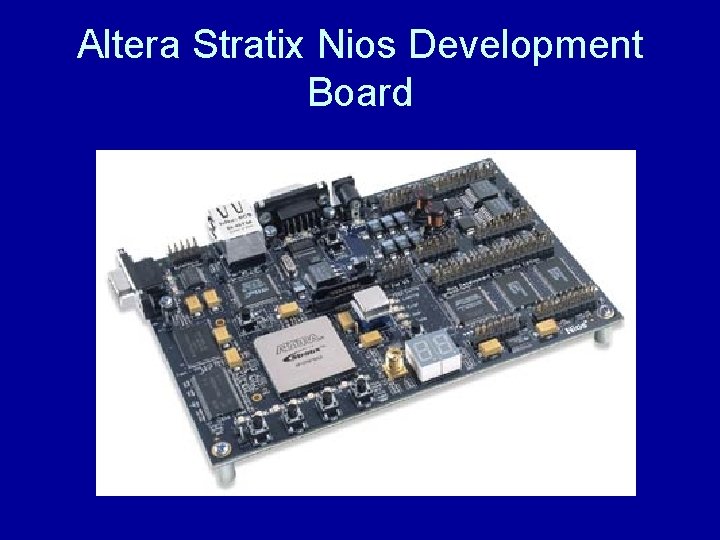
Altera Stratix Nios Development Board
Altera Stratix Nios Development Board • Stratix EP 1 S 10 F 780 C 6 – 10, 570 Logic Elements – 920 Kb on-chip memory • Provide hardware platform for developing embedded system – Comes pre-programmed with a 32 -bit Nios processor reference design
Altera Staratix Nios Development Board • 8 MB of flash Memory, 1 MB of static RAM, 16 MB of SDRAM • On-board Ethernet MAC/PHY device • Compact Flash connector hearder • Two RS-232 DB 9 serial ports • 50 MHz oscillator and zero-skew clock distribution circuitry • Four push-button switches • Dual 7 -segment LED display
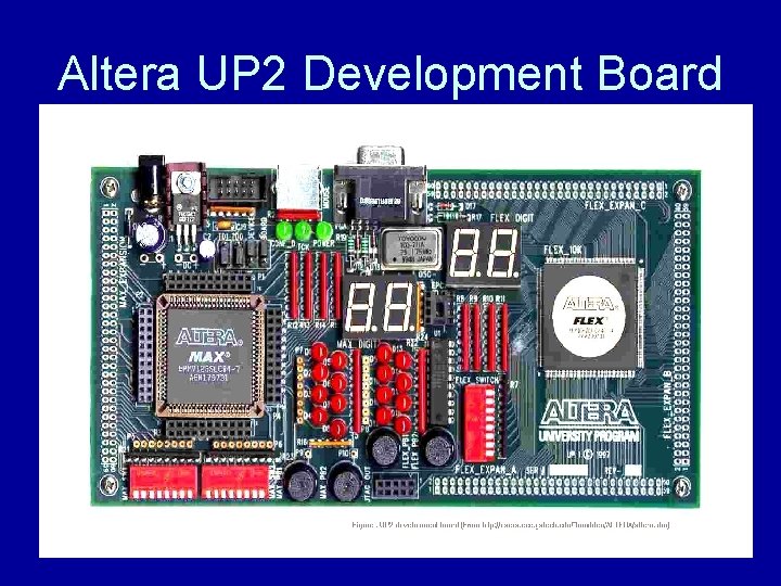
Altera UP 2 Development Board
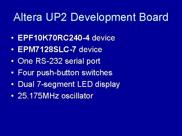
Altera UP 2 Development Board • • • EPF 10 K 70 RC 240 -4 device EPM 7128 SLC-7 device One RS-232 serial port Four push-button switches Dual 7 -segment LED display 25. 175 MHz oscillator
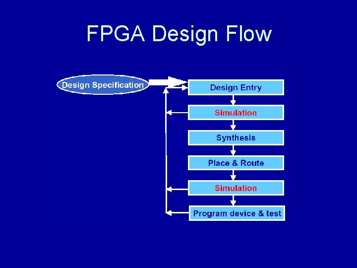
FPGA Design Flow
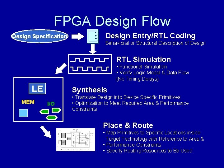
FPGA Design Flow Design Specification Design Entry/RTL Coding Behavioral or Structural Description of Design RTL Simulation • Functional Simulation • Verify Logic Model & Data Flow (No Timing Delays) LE MEM Synthesis I/O • Translate Design into Device Specific Primitives • Optimization to Meet Required Area & Performance Constraints Place & Route • Map Primitives to Specific Locations inside Target Technology with Reference to Area & • Performance Constraints • Specify Routing Resources to Be Used
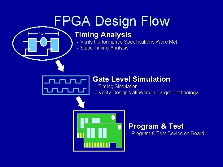
FPGA Design Flow tclk Timing Analysis - Verify Performance Specifications Were Met - Static Timing Analysis Gate Level Simulation - Timing Simulation - Verify Design Will Work in Target Technology Program & Test - Program & Test Device on Board
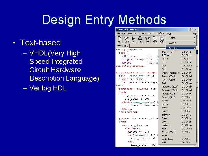
Design Entry Methods • Text-based – VHDL(Very High Speed Integrated Circuit Hardware Description Language) – Verilog HDL
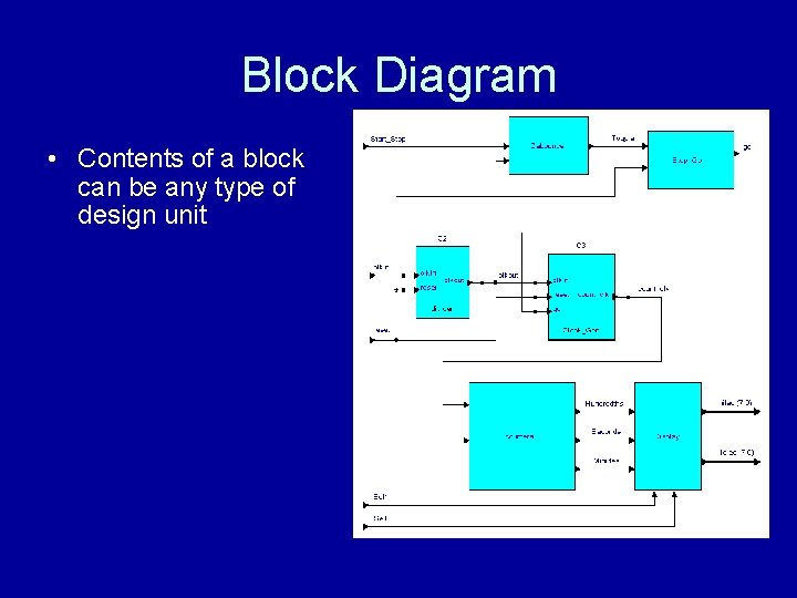
Block Diagram • Contents of a block can be any type of design unit
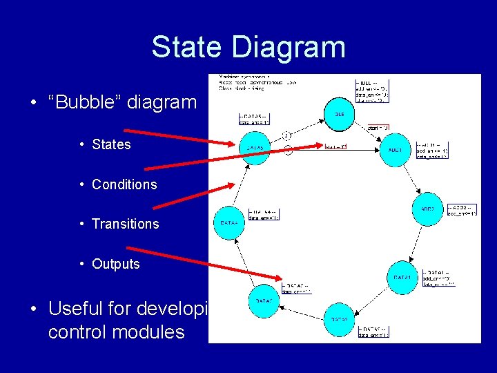
State Diagram • “Bubble” diagram • States • Conditions • Transitions • Outputs • Useful for developing control modules
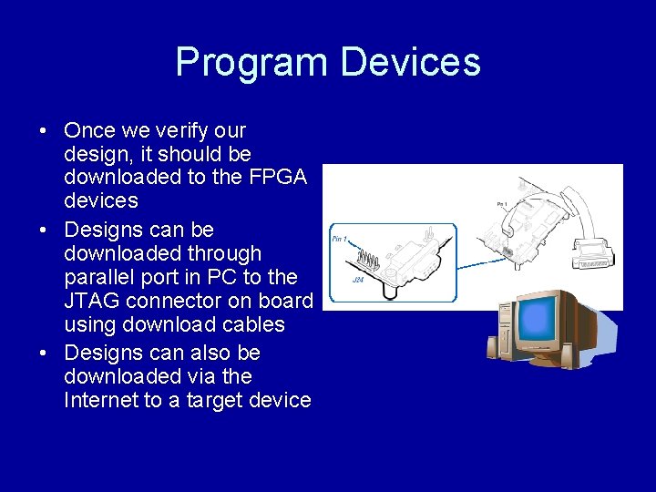
Program Devices • Once we verify our design, it should be downloaded to the FPGA devices • Designs can be downloaded through parallel port in PC to the JTAG connector on board using download cables • Designs can also be downloaded via the Internet to a target device
Introduction to Altera Design Software • Software & Development Tools: – Quartus II • Stratix II, Stratix GX, Cyclone, APEX II, APEX 20 K/E/C, Excalibur, & Mercury Devices • FLEX 10 K/A/E, ACEX 1 K, FLEX 6000, MAX 7000 S/AE/B, MAX 3000 A Devices – Quartus II Web Edition • Free Version • Not All Features & Devices Included – MAX+PLUS® II • All FLEX, ACEX, & MAX Devices
Quartus II Development System • • Fully-Integrated Design Tool Multiple Design Entry Methods Logic Synthesis Place & Route Simulation Timing & Power Analysis Device Programming
More Features • • Mega. Wizard® & SOPC Builder Design Tools Logic. Lock™ Optimization Tool Native. Link® 3 rd-Party EDA Tool Integration Integrated Embedded Software Development Signal. Tap® II & Signal. Probe™ Debug Tools Windows, Solaris, HPUX, & Linux Support Node-Locked & Network Licensing Options Revision Control Interface
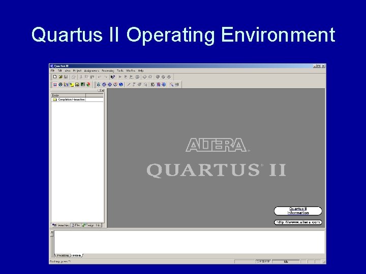
Quartus II Operating Environment
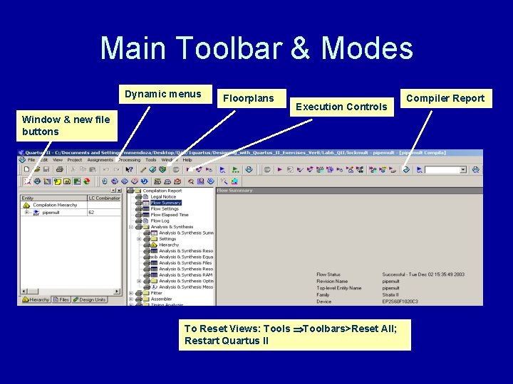
Main Toolbar & Modes Dynamic menus Floorplans Execution Controls Window & new file buttons To Reset Views: Tools Toolbars>Reset All; Restart Quartus II Compiler Report
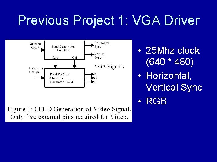
Previous Project 1: VGA Driver • 25 Mhz clock (640 * 480) • Horizontal, Vertical Sync • RGB
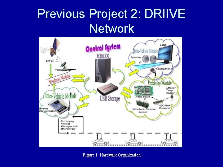
Previous Project 2: DRIIVE Network Figure 1: Hardware Organization
Summary • Prerequisite – Electronics and circuits – Digital logic design – VHDL (VHSIC Hardware Description Language) • FPGA – Combine technologies in hardware & software – Benefits
- Slides: 44