An Implementation of the Discrete Fourier Transform on

- Slides: 20

An Implementation of the Discrete Fourier Transform on a Reconfigurable Processor By Michael J. White 1, 2* and Clay Gloster, Jr. , Ph. D. , P. E. 1 1 Department of Electrical & Computer Engineering Howard University 2300 Sixth Street, NW Washington, DC 20059 2 NASA/ Goddard Space Flight Center Code 564 Greenbelt, MD 20771 Michael. J. White@nasa. gov, cgloster@howard. edu *Member, AIAA MAPLD Conference Washington, DC September 9 -11, 2003 White and Gloster 1 P 74

Outline of the Presentation • Introduction • The Discrete Fourier Transform (DFT) • A Sample Reconfigurable Processor • A Floating Point DFT Core • Experimental Results • Conclusions and Future Work White and Gloster 2 P 74

Introduction • A reconfigurable computing (RC) system is a hardware/software data processing system that combines the flexibility of a general purpose processors with the speed of application specific processors. • Several applications have been mapped onto RC systems demonstrating an order of magnitude speedup over existing solutions running on a general purpose processor. • In the past, RC systems contained very limited hardware resources. As a result, few complex applications, i. e. floating point arithmetic, could benefit from the potential speedup offered by RC systems. • To the knowledge of the authors, few have published papers on implementing the DFT on a Field Programmable Gate Array(FPGA) using floating point arithmetic. White and Gloster 3 P 74

Motivation • At Goddard, there is an interest in control algorithms, that in part use the DFT. • These algorithm should not be constrained to require the input data to be of size 2^n. • The goal is to be able to process a 512 x 512 floating point array in 0. 01 seconds. White and Gloster 4 P 74

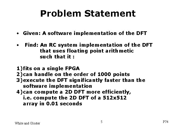
Problem Statement • Given: A software implementation of the DFT • Find: An RC system implementation of the DFT that uses floating point arithmetic such that it : 1) fits on a single FPGA 2) can handle on the order of 1000 points 3) execute the DFT significantly faster than the software implementation 4) can compute a 2 D DFT more efficiently, i. e. compute the 2 D DFT of a 512 x 512 array in 0. 01 seconds White and Gloster 5 P 74

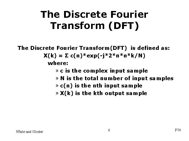
The Discrete Fourier Transform (DFT) The Discrete Fourier Transform(DFT) is defined as: X(k) = Σ c(n)*exp(-j*2*π*n*k/N) where: » c is the complex input sample » N is the total number of input samples » c(n) is the nth input sample » X(k) is the kth output sample White and Gloster 6 P 74

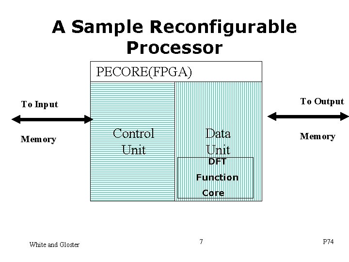
A Sample Reconfigurable Processor PECORE(FPGA) To Output To Input Memory Control Unit Data Unit Memory DFT Function Core White and Gloster 7 P 74

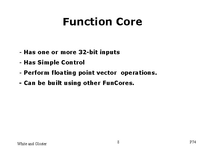
Function Core - Has one or more 32 -bit inputs - Has Simple Control - Perform floating point vector operations. - Can be built using other Fun. Cores. White and Gloster 8 P 74

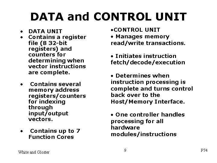
DATA and CONTROL UNIT • DATA UNIT • Contains a register file (8 32 -bit registers) and counters for determining when vector instructions are complete. • • Contains several memory address registers/counters for indexing through input/output vectors. Contains up to 7 Function Cores White and Gloster • CONTROL UNIT • Manages memory read/write transactions. • Initiates instruction fetch/decode/execution • Determines when instruction processing is complete and turns control back over to the Host/Memory Interface. • One controller handles processing for all hardware modules/instructions 9 P 74

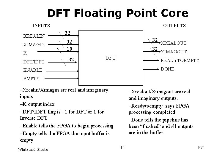
DFT Floating Point Core INPUTS XREALIN XIMAGIN K DFT/IDFT OUTPUTS 32 32 32 10 32 XREALOUT 32 XIMAGOUT DFT READYTOEMPTY DONE ENABLE EMPTY –Xrealin/Ximagin are real and imaginary inputs –K output index –DFT/IDFT flag is – 1 for DFT or 1 for Inverse DFT –Enable tells the FPGA to begin processing –Empty tells the FPGA the input buffer is empty White and Gloster –Xrealout/Ximagout are real and imaginary outputs. –Readytoempty says FPGA processing completed –Done tells the pipeline has been “flushed” and all outputs are in the buffer. 10 P 74

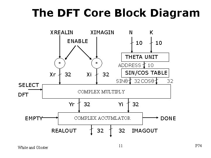
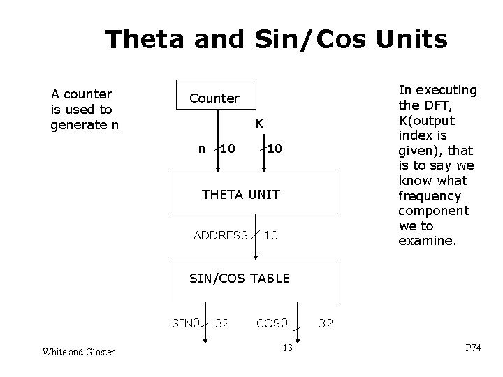
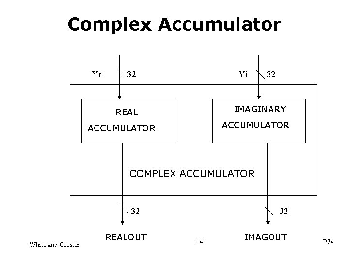
The DFT Core Block Diagram XREALIN XIMAGIN N ENABLE K 10 10 THETA UNIT * Xr * 32 Xi ADDRESS SINθ Yr 32 Yi 32 32 DONE COMPLEX ACCUMLATOR REALOUT White and Gloster 32 COSθ COMPLEX MULTIPLY DFT EMPTY SIN/COS TABLE 32 SELECT 10 32 32 11 IMAGOUT P 74

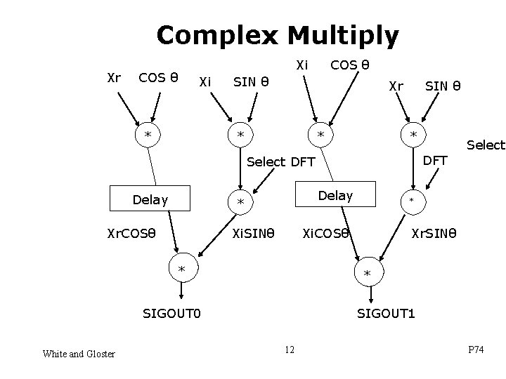
Complex Multiply Xr COS θ Xi Xi * COS θ SIN θ Xr * * SIN θ * DFT Select DFT Delay * Xr. COSθ Xi. SINθ Xr. SINθ * SIGOUT 0 White and Gloster * Xi. COSθ * Select SIGOUT 1 12 P 74

Theta and Sin/Cos Units A counter is used to generate n In executing the DFT, K(output index is given), that is to say we know what frequency component we to examine. Counter K n 10 10 THETA UNIT ADDRESS 10 SIN/COS TABLE SINθ White and Gloster 32 COSθ 13 32 P 74

Complex Accumulator Yr 32 Yi 32 IMAGINARY REAL ACCUMULATOR COMPLEX ACCUMULATOR 32 White and Gloster REALOUT 32 14 IMAGOUT P 74

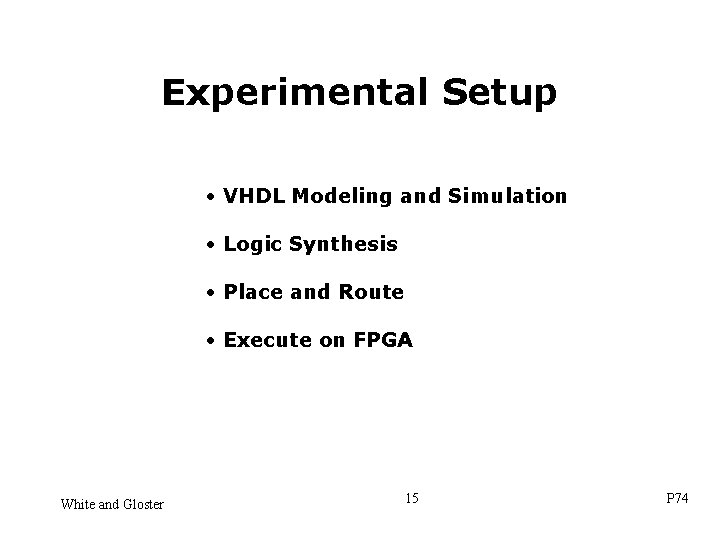
Experimental Setup • VHDL Modeling and Simulation • Logic Synthesis • Place and Route • Execute on FPGA White and Gloster 15 P 74

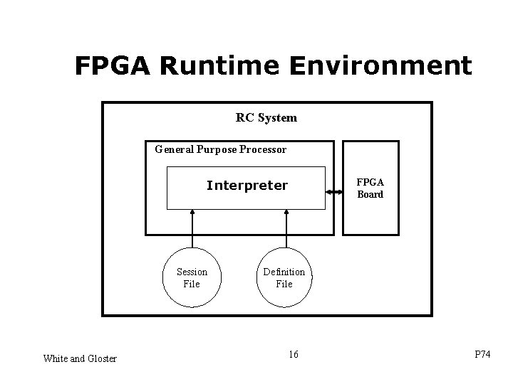
FPGA Runtime Environment RC System General Purpose Processor FPGA Board Interpreter Session File White and Gloster Definition File 16 P 74

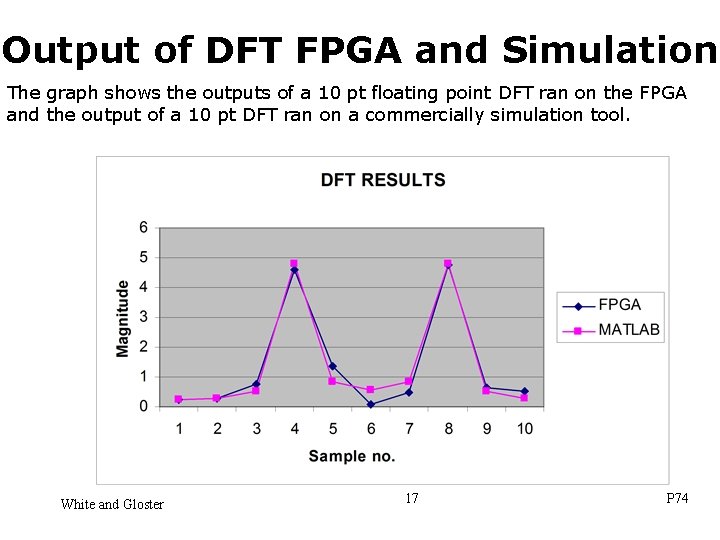
Output of DFT FPGA and Simulation The graph shows the outputs of a 10 pt floating point DFT ran on the FPGA and the output of a 10 pt DFT ran on a commercially simulation tool. White and Gloster 17 P 74

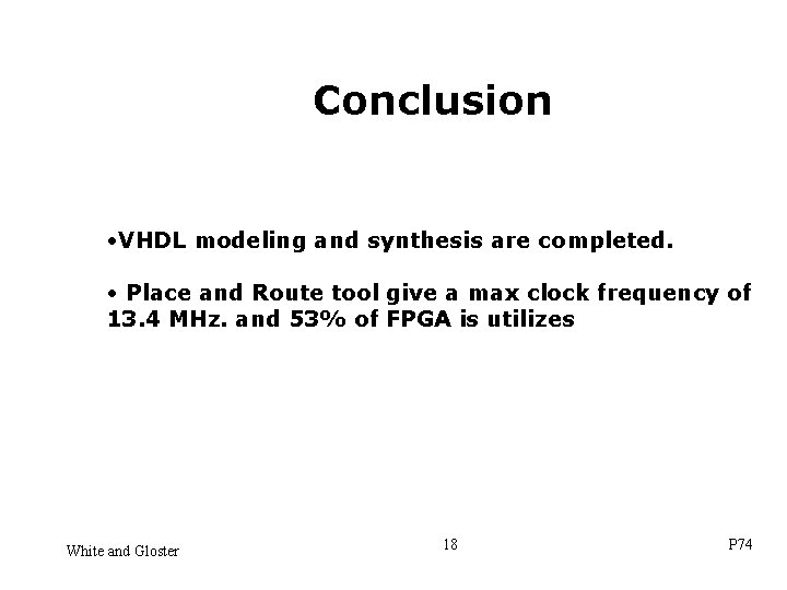
Conclusion • VHDL modeling and synthesis are completed. • Place and Route tool give a max clock frequency of 13. 4 MHz. and 53% of FPGA is utilizes White and Gloster 18 P 74

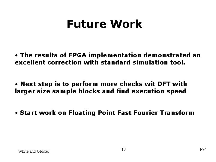
Future Work • The results of FPGA implementation demonstrated an excellent correction with standard simulation tool. • Next step is to perform more checks wit DFT with larger size sample blocks and find execution speed • Start work on Floating Point Fast Fourier Transform White and Gloster 19 P 74

Acknowledgement • The authors would like to thank NASA/ Goddard Space Flight Center for its support of this project. In particular, we give thanks to: • Mr. Thomas Flatley and Mr. Semion Kizhner for initiating the project. • Mr. Robert Kasa and Mr. Wesley Powell for their management support. • Dr. John Day for providing the spark that put everything together. White and Gloster 20 P 74