An Experimental Study of Tester Yield and Defect

- Slides: 20

An Experimental Study of Tester Yield and Defect Coverage Jose T. de Sousa INESC/IST, Technical University of Lisbon 1000 Lisboa, Portugal jose. desousa@inesc. pt Vishwani D. Agrawal Circuit and Systems Research Lab Agere Systems, Murray Hill, NJ 07974 USA va@agere. com IEEE International Test Synthesis Workshop, Santa Barbara, CA March 25, 2001 de Sousa-Agrawal/ITSW 01 1

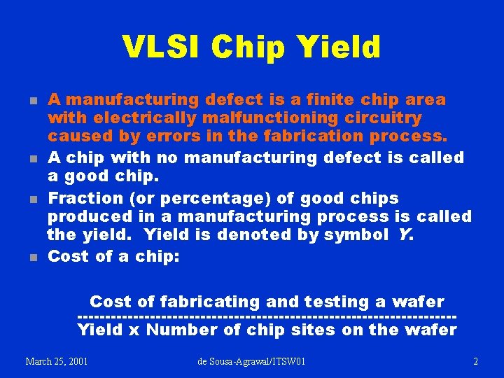
VLSI Chip Yield n n A manufacturing defect is a finite chip area with electrically malfunctioning circuitry caused by errors in the fabrication process. A chip with no manufacturing defect is called a good chip. Fraction (or percentage) of good chips produced in a manufacturing process is called the yield. Yield is denoted by symbol Y. Cost of a chip: Cost of fabricating and testing a wafer ----------------------------------Yield x Number of chip sites on the wafer March 25, 2001 de Sousa-Agrawal/ITSW 01 2

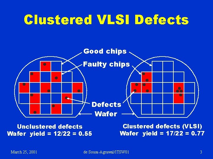
Clustered VLSI Defects Good chips Faulty chips Defects Wafer Unclustered defects Wafer yield = 12/22 = 0. 55 March 25, 2001 Clustered defects (VLSI) Wafer yield = 17/22 = 0. 77 de Sousa-Agrawal/ITSW 01 3

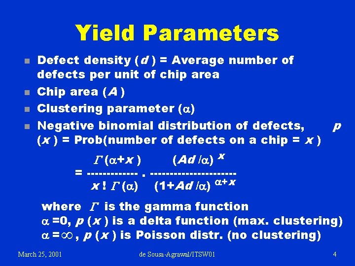
Yield Parameters n n Defect density (d ) = Average number of defects per unit of chip area Chip area (A ) Clustering parameter (a) Negative binomial distribution of defects, (x ) = Prob(number of defects on a chip = x ) p (Ad /a) x = -----------x ! G (a) (1+Ad /a) a+x G (a+x ) where G is the gamma function a =0, p (x ) is a delta function (max. clustering) a = ¥ , p (x ) is Poisson distr. (no clustering) March 25, 2001 de Sousa-Agrawal/ITSW 01 4

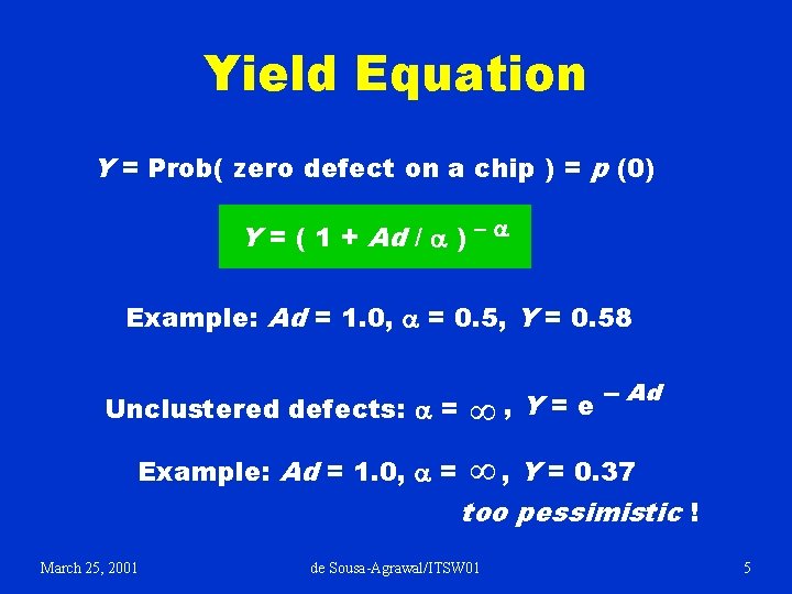
Yield Equation Y = Prob( zero defect on a chip ) = p (0) Y = ( 1 + Ad / a ) - a Example: Ad = 1. 0, a = 0. 5, Y = 0. 58 Unclustered defects: a = Example: Ad = 1. 0, a = ¥, Y=e -- Ad ¥ , Y = 0. 37 too pessimistic ! March 25, 2001 de Sousa-Agrawal/ITSW 01 5

Defect Level or Reject Ratio n n Defect level (DL) is the ratio of faulty chips among the chips that pass tests. DL is measured as parts per million (ppm). DL is a measure of the effectiveness of tests. DL is a quantitative measure of the manufactured product quality. For commercial VLSI chips a DL greater than 500 ppm is considered unacceptable. March 25, 2001 de Sousa-Agrawal/ITSW 01 6

Determination of DL n n From field return data: Chips failing in the field are returned to the manufacturer. The number of returned chips normalized to one million chips shipped is the DL. From test data: Fault coverage of tests and chip fallout rate are analyzed. A modified yield model is fitted to the fallout data to estimate the DL. March 25, 2001 de Sousa-Agrawal/ITSW 01 7

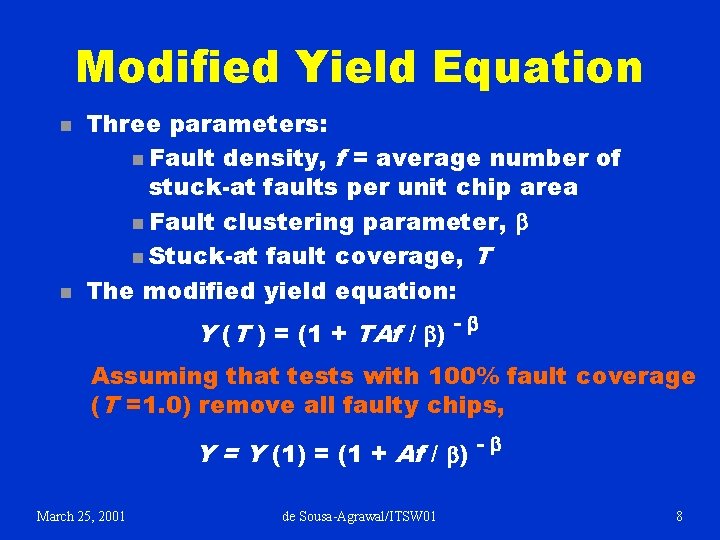
Modified Yield Equation n n Three parameters: n Fault density, f = average number of stuck-at faults per unit chip area n Fault clustering parameter, b n Stuck-at fault coverage, T The modified yield equation: Y (T ) = (1 + TAf / b) - b Assuming that tests with 100% fault coverage (T =1. 0) remove all faulty chips, Y = Y (1) = (1 + Af / b) - b March 25, 2001 de Sousa-Agrawal/ITSW 01 8

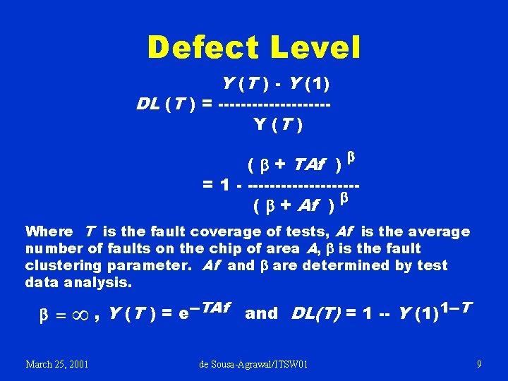
Defect Level Y (T ) - Y (1) DL (T ) = ----------Y (T ) b ( b + TAf ) = 1 - ----------b ( b + Af ) Where T is the fault coverage of tests, Af is the average number of faults on the chip of area A, b is the fault clustering parameter. Af and b are determined by test data analysis. b = ¥ , Y (T ) = e--TAf March 25, 2001 and DL(T) = 1 -- Y (1)1 --T de Sousa-Agrawal/ITSW 01 9

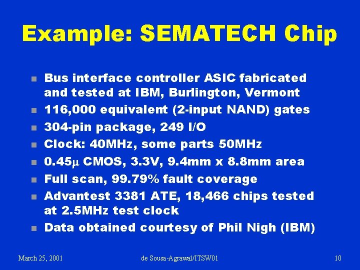
Example: SEMATECH Chip n n n n Bus interface controller ASIC fabricated and tested at IBM, Burlington, Vermont 116, 000 equivalent (2 -input NAND) gates 304 -pin package, 249 I/O Clock: 40 MHz, some parts 50 MHz 0. 45 m CMOS, 3. 3 V, 9. 4 mm x 8. 8 mm area Full scan, 99. 79% fault coverage Advantest 3381 ATE, 18, 466 chips tested at 2. 5 MHz test clock Data obtained courtesy of Phil Nigh (IBM) March 25, 2001 de Sousa-Agrawal/ITSW 01 10

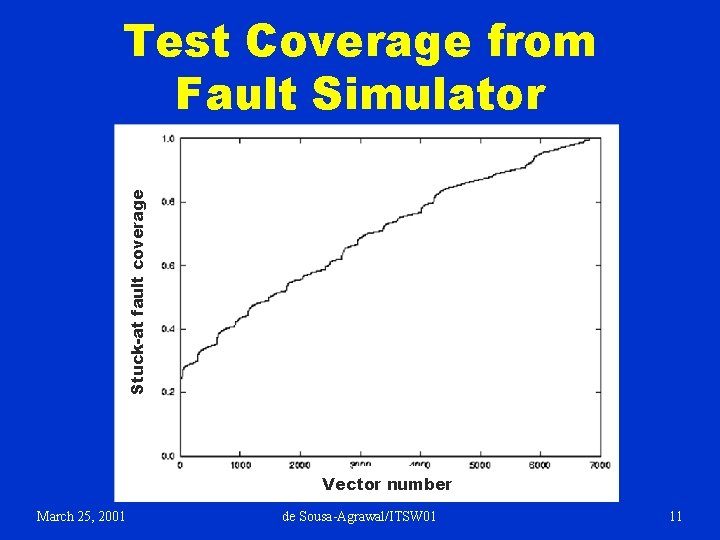
Stuck-at fault coverage Test Coverage from Fault Simulator Vector number March 25, 2001 de Sousa-Agrawal/ITSW 01 11

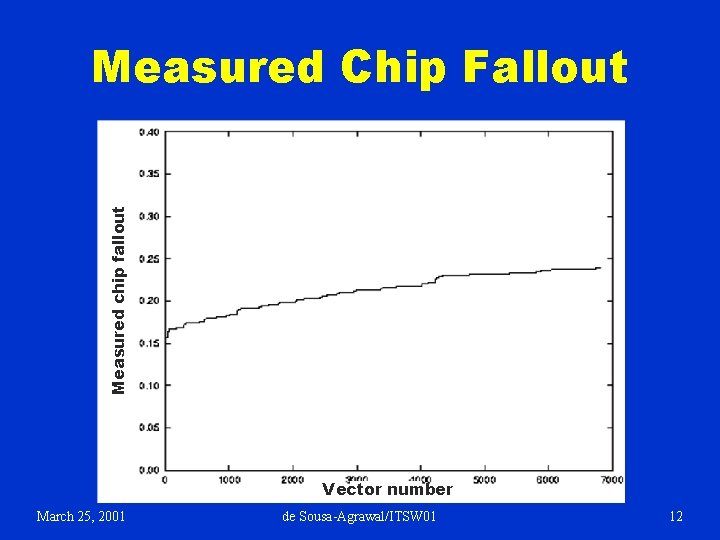
Measured chip fallout Measured Chip Fallout Vector number March 25, 2001 de Sousa-Agrawal/ITSW 01 12

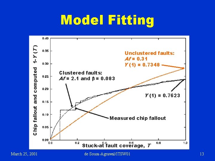
Chip fallout and computed 1 -Y (T ) Model Fitting Unclustered faults: Af = 0. 31 Y (1) = 0. 7348 Clustered faults: Af = 2. 1 and b = 0. 083 Y (1) = 0. 7623 Measured chip fallout Stuck-at fault coverage, T March 25, 2001 de Sousa-Agrawal/ITSW 01 13

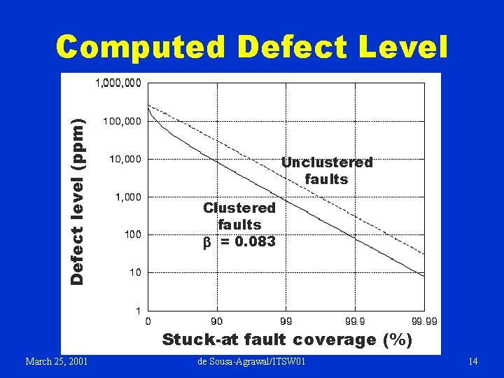
Defect level (ppm) Computed Defect Level Unclustered faults Clustered faults b = 0. 083 Stuck-at fault coverage (%) March 25, 2001 de Sousa-Agrawal/ITSW 01 14

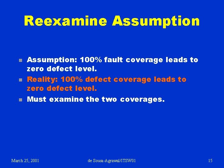
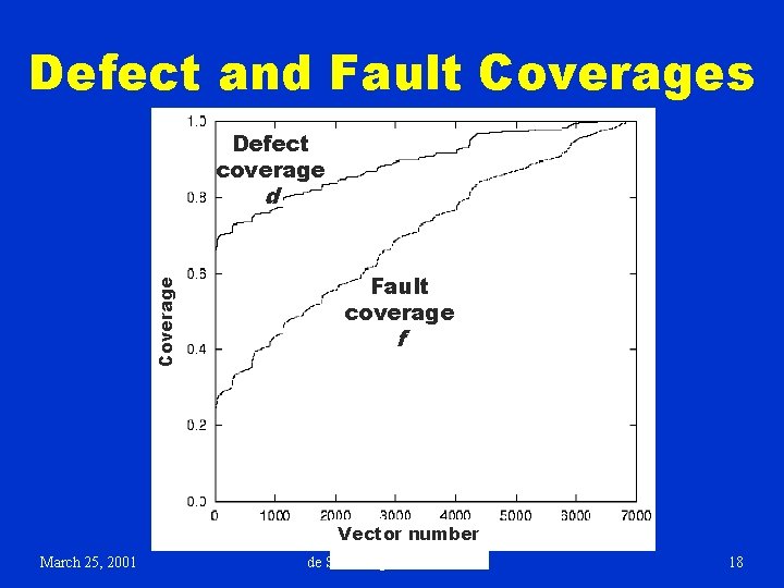
Reexamine Assumption n Assumption: 100% fault coverage leads to zero defect level. Reality: 100% defect coverage leads to zero defect level. Must examine the two coverages. March 25, 2001 de Sousa-Agrawal/ITSW 01 15

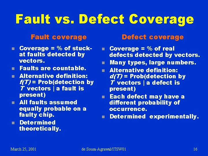
Fault vs. Defect Coverage Fault coverage n n n Coverage = % of stuckat faults detected by vectors. Faults are countable. Alternative definition: f(T) = Prob(detection by T vectors | a fault is present) All faults assumed equally probable on a faulty chip. Determined theoretically. March 25, 2001 Defect coverage n n n Coverage = % of real defects detected by vectors. Many types, large numbers. Alternative definition: d(T) = Prob(detection by T vectors | a defect is present) Each defect may have a different probability of occurrence. Determined experimentally. de Sousa-Agrawal/ITSW 01 16

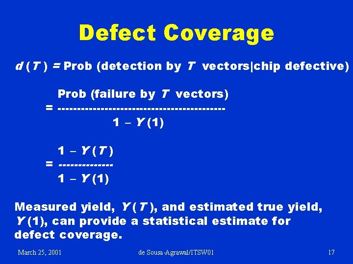
Defect Coverage d (T ) = Prob (detection by T vectors|chip defective) Prob (failure by T vectors) = ---------------------1 – Y (1) 1 – Y (T ) = -------1 – Y (1) Measured yield, Y (T ), and estimated true yield, Y (1), can provide a statistical estimate for defect coverage. March 25, 2001 de Sousa-Agrawal/ITSW 01 17

Defect and Fault Coverages Defect coverage Coverage d Fault coverage f Vector number March 25, 2001 de Sousa-Agrawal/ITSW 01 18

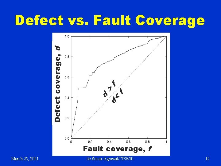
Defect coverage, d Defect vs. Fault Coverage d > f d< f Fault coverage, f March 25, 2001 de Sousa-Agrawal/ITSW 01 19

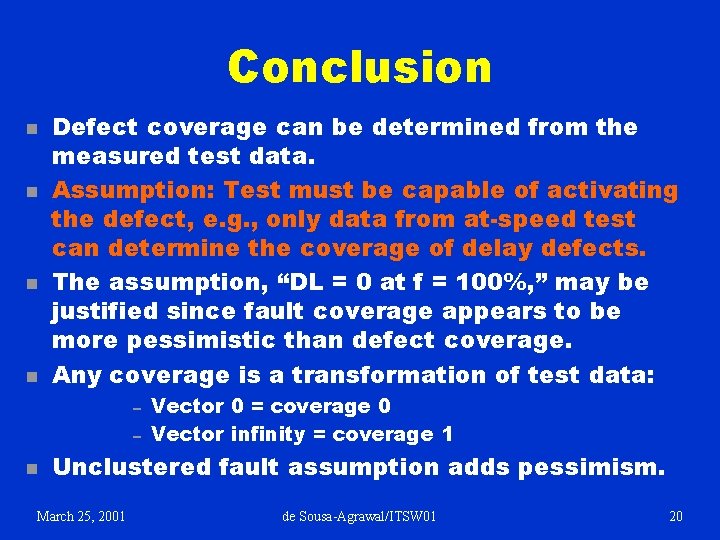
Conclusion n n Defect coverage can be determined from the measured test data. Assumption: Test must be capable of activating the defect, e. g. , only data from at-speed test can determine the coverage of delay defects. The assumption, “DL = 0 at f = 100%, ” may be justified since fault coverage appears to be more pessimistic than defect coverage. Any coverage is a transformation of test data: – – n Vector 0 = coverage 0 Vector infinity = coverage 1 Unclustered fault assumption adds pessimism. March 25, 2001 de Sousa-Agrawal/ITSW 01 20