An Equivalent Circuit Model for a Faraday Cage


- Slides: 2

An Equivalent Circuit Model for a Faraday Cage Substrate Crosstalk Isolation Structure Joyce H. Wu (jowu@mtl. mit. edu) and Jesús A. del Alamo Massachusetts Institute of Technology Motivation Faraday Cage Isolation Structure Noisy or sensitive devices/circuits System-on-Chip Al A/D Al Digital Logic A/D Silicon nitride Si substrate Faraday cage Analog/RF A/D Substrate-Via Technology Key Features 75 -100 µm Silicon nitride Noisy Substrate Si Substrate crosstalk is considered one of the biggest problems in mixed-signal circuits Ta-Ti-Cu seed Cu Grounded via • Deep reactive ion etch (DRIE) • Silicon nitride barrier liner • Electroplated Cu fills via Cu ground plane Fabrication (4) e-beam deposition of Ta-Ti-Cu seed on backside (1) photoresist mask patterning (7) Cu CMP frontside for a flush surface Si (5) Cu electroplating to close bottom of via (2) DRIE through the substrate (3) photoresist strip, silicon nitride deposition from front and backside (6) Cu electroplating to fill via (8) Al e-beam deposition and patterning to form contact to via 12 µm Cu 12 µm x 100 µm vias before Cu CMP step (aspect ratio = 8) Measurements Test Structures Reference Substrate-Via Impedance Faraday Cage Test Structure Substrate Via Model: Faraday cage Ground 100 µm Signal Im(Z 11) 100 µm 200 µm Re(Z 11) Rv 70 µm Z 11 Ground Lv Transmitter Receiver Substrate via Faraday Cage Substrate Noise Isolation Reference At 100 µm distance, on average: Faraday Cage Air Substrate thickness=77 µm Separation dist. =100 µm Via separation=10 µm Via diameter=10 µm 1 GHz: 41 d. B improvement 10 GHz: 30 d. B improvement 50 GHz: 16 d. B improvement Simulation Measured

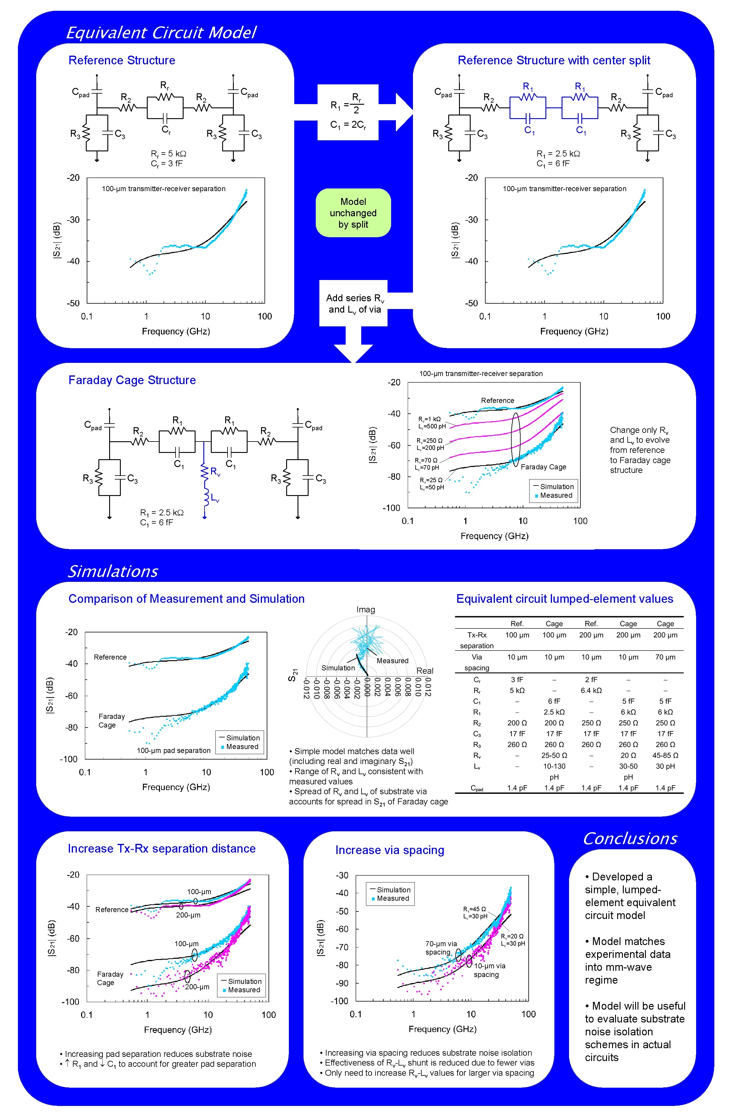
Equivalent Circuit Model Reference Structure Cpad Rr R 2 R 3 Reference Structure with center split R 2 Cr C 3 Cpad Rr R 1 = 2 C 1 = 2 Cr C 3 R 2 R 3 C 3 R 1 C 1 Rr = 5 k Cr = 3 f. F R 2 R 3 Cpad C 3 R 1 = 2. 5 k C 1 = 6 f. F 100 -µm transmitter-receiver separation Model unchanged by split Add series Rv and Lv of via 100 -µm transmitter-receiver separation Faraday Cage Structure Reference Cpad R 2 R 1 C 1 R 3 Rv C 3 Rv=1 kΩ Lv=500 p. H Cpad R 2 Rv=250 Ω Lv=200 p. H Rv=70 Ω Lv=70 p. H C 1 R 3 C 3 Faraday Cage Rv=25 Ω Lv=50 p. H Change only Rv and Lv to evolve from reference to Faraday cage structure Simulation Measured Lv R 1 = 2. 5 k C 1 = 6 f. F Simulations Comparison of Measurement and Simulation Imag Reference S 21 Equivalent circuit lumped-element values Simulation Measured Real Faraday Cage 100 -µm pad separation Simulation Measured Increase Tx-Rx separation distance Increase via spacing 200 -µm • Developed a simple, lumpedelement equivalent circuit model Rv=45 Ω Lv=30 p. H 100 -µm Faraday Cage Conclusions Simulation Measured 100 -µm Reference • Simple model matches data well (including real and imaginary S 21) • Range of Rv and Lv consistent with measured values • Spread of Rv and Lv of substrate via accounts for spread in S 21 of Faraday cage 70 -µm via spacing Simulation Measured • Increasing pad separation reduces substrate noise • R 1 and C 1 to account for greater pad separation Rv=20 Ω Lv=30 p. H 10 -µm via spacing • Increasing via spacing reduces substrate noise isolation • Effectiveness of Rv-Lv shunt is reduced due to fewer vias • Only need to increase Rv-Lv values for larger via spacing • Model matches experimental data into mm-wave regime • Model will be useful to evaluate substrate noise isolation schemes in actual circuits