An Avalanche Diode Array with Bulk Integrated Quench
An Avalanche Diode Array with Bulk Integrated Quench Resistors for Single Photon Detection R. H. Richter 1) , L. Andricek 1) 1) , G. Lutz MPI für Physik, 2) 2) , H. -G. Moser 1) , J. Ninkovic 1) PN Sensor Gmb. H 1. Silicon Photomultiplier – brief introduction 2. Polysilicon quench resistors - a cost driver in a Si. PM technology 3. An alternative Si. PM array – aimed for mass production (no backside illumination) 4. Wafer bonding 5. Discussion 6. Next steps 10. 12. 2007 R. H. Richter, ILC - Meeting
What is a Silicon Photomultipler ? Array of segmented Avalanche diodes each of them operated in Geigermode. All individual diodes (sub pixel) are usually connected in parallel to 1 amplifier What is gained ? - photon counting capability with high dynamic range - high accessebility (no dead time at low rates) - shorter response times No Gain in: - position resolution Name Si. PM is misleading - often called GAPD 10. 12. 2007 R. H. Richter, ILC - Meeting
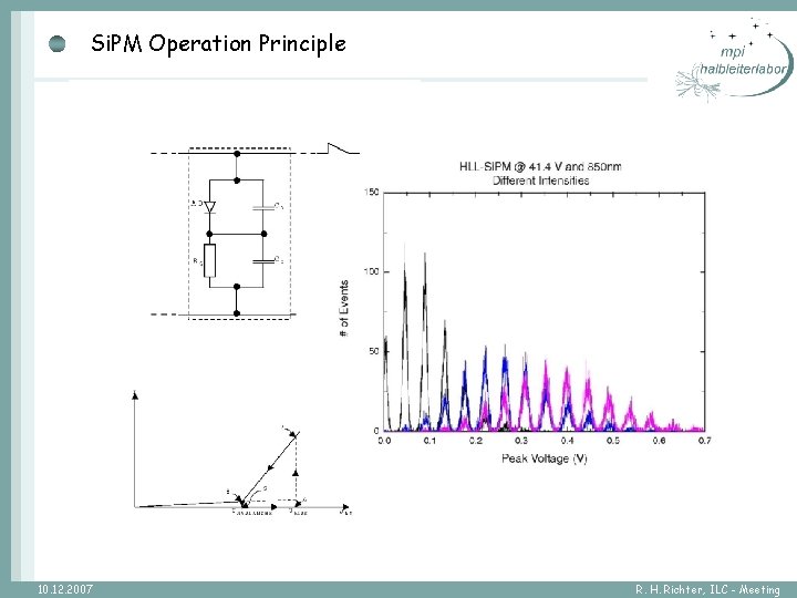
Si. PM Operation Principle 10. 12. 2007 R. H. Richter, ILC - Meeting
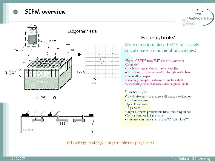
SIPM overview Dolgoshein et al E. Lorenz, Light 07 Technology: epitaxy, 4 implantations, polysilicon 10. 12. 2007 R. H. Richter, ILC - Meeting
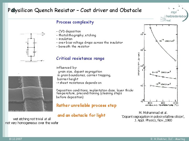
Polysilicon Quench Resistor – Cost driver and Obstacle Process complexity - CVD deposition - Photolithography, etching - insulation - over bias voltage drops across the insulator - beneath the resistor Critical resistance range influenced by: grain size, dopant segragation in grain boundaries, carrier trapping, barrier height -> sheet resistance depends on Deposition conditions, implantation dose, layer thickness, annealing temperature, preconditioning (cleaning steps before deposition) Rather unreliable process step and an obstacle for light wet etching not trivial at all not very homogeneous over the wafer 10. 12. 2007 M. Mohammad et al. ‘Dopant segragation in polycrystalline silicon‘, J. Appl. Physics, Nov. , 1980 R. H. Richter, ILC - Meeting
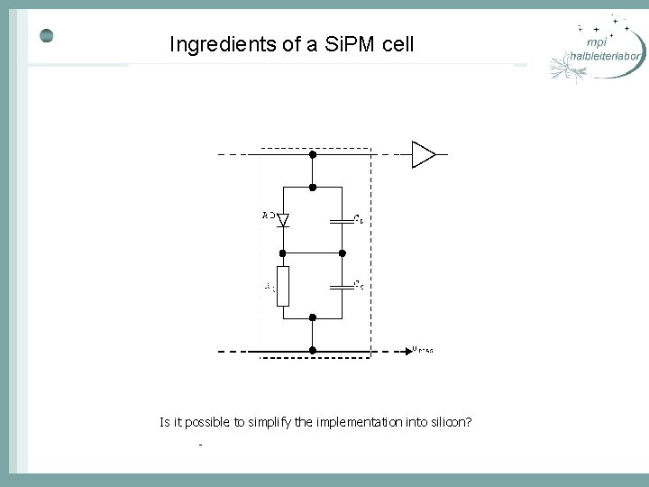
Ingredients of a Si. PM cell Is it possible to simplify the implementation into silicon?
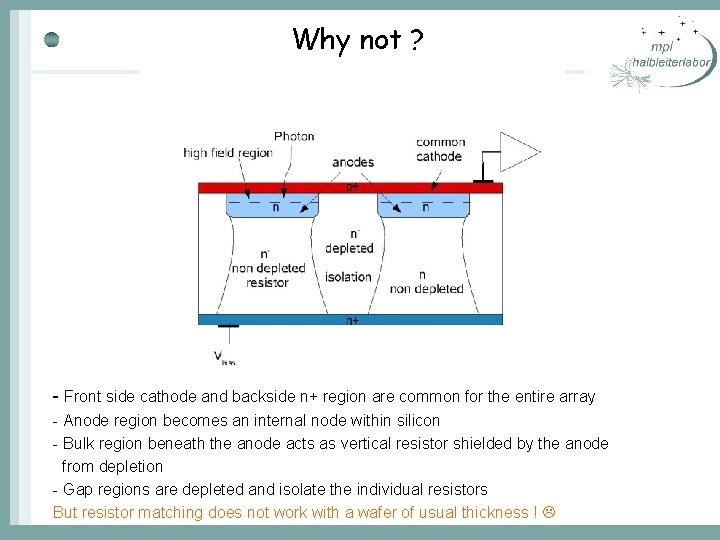
Why not ? - Front side cathode and backside n+ region are common for the entire array - Anode region becomes an internal node within silicon - Bulk region beneath the anode acts as vertical resistor shielded by the anode from depletion - Gap regions are depleted and isolate the individual resistors But resistor matching does not work with a wafer of usual thickness !

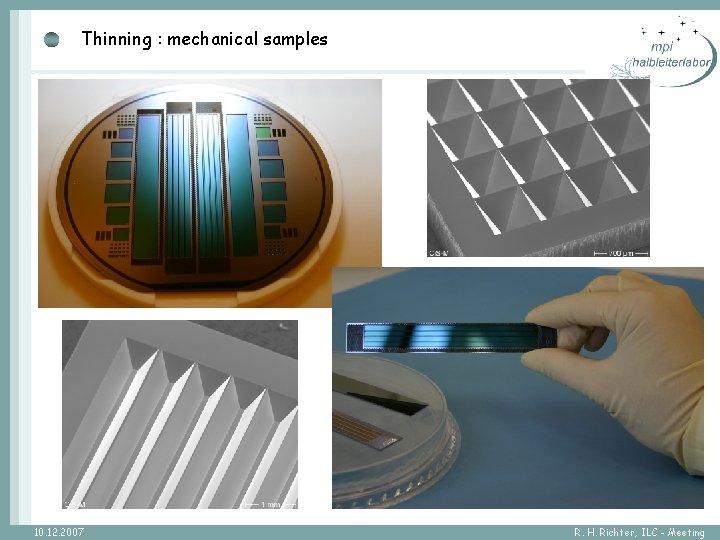
Processing thin detectors (50 mm) a) oxidation and back side implant of top wafer c) process passivation Top Wafer open backside passivation b) wafer bonding and grinding/polishing of top wafer 10. 12. 2007 d) deep etching opens "windows" in handle wafer R. H. Richter, ILC - Meeting
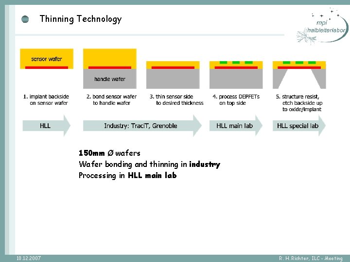
Thinning Technology 150 mm Ø wafers Wafer bonding and thinning in industry Processing in HLL main lab 10. 12. 2007 R. H. Richter, ILC - Meeting
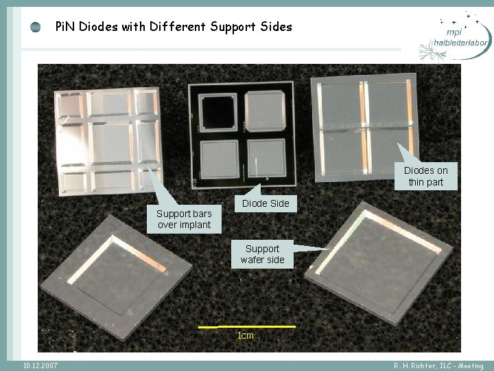
Pi. N Diodes with Different Support Sides Diodes on thin part Support bars over implant Diode Side Support wafer side 1 cm 10. 12. 2007 R. H. Richter, ILC - Meeting
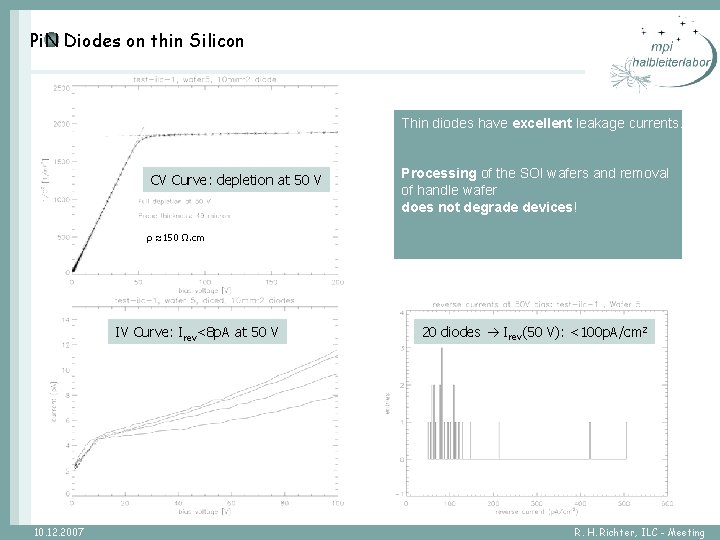
Pi. N Diodes on thin Silicon Thin diodes have excellent leakage currents. CV Curve: depletion at 50 V Processing of the SOI wafers and removal of handle wafer does not degrade devices! ρ ≈150 Ω. cm IV Curve: Irev<8 p. A at 50 V 10. 12. 2007 20 diodes Irev(50 V): <100 p. A/cm 2 R. H. Richter, ILC - Meeting
Thinning : mechanical samples 10. 12. 2007 R. H. Richter, ILC - Meeting
Wafer bonding technique is a well established technology. SOITEC-TRACIT (France), ICEMOS (Ireland) It provides the means for the quench resistor adoption ! two parameters: top wafer thickness doping level Experience with processing at HLL 10. 12. 2007 R. H. Richter, ILC - Meeting
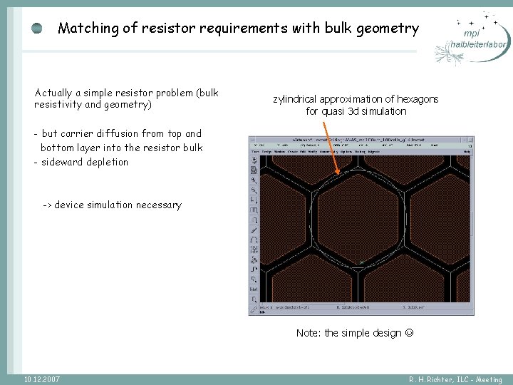
Matching of resistor requirements with bulk geometry Actually a simple resistor problem (bulk resistivity and geometry) zylindrical approximation of hexagons for quasi 3 d simulation - but carrier diffusion from top and bottom layer into the resistor bulk - sideward depletion -> device simulation necessary Note: the simple design 10. 12. 2007 R. H. Richter, ILC - Meeting
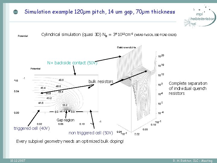
Simulation example 120µm pitch, 14 um gap, 70µm thickness Cylindrical simulation (quasi 3 D) NB = 3*1012 cm-2 (WIAS-Te. SCA, ISE-TCAD DIOS) N+ backside contact (50 V) bulk resistors Complete separation of individual quench resistors Gap region triggered cell (40 V) non triggered cell (50 V) Every subpixel geometry needs an optimized bulk doping! 10. 12. 2007 R. H. Richter, ILC - Meeting
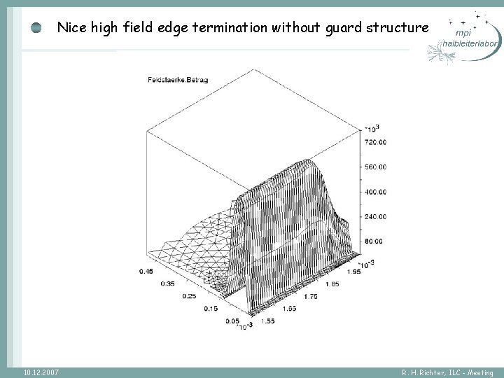
Nice high field edge termination without guard structure 10. 12. 2007 R. H. Richter, ILC - Meeting

Signal height – given by (bulk) coupling capacitance 8 x 10 -14 As Ccoupl = 14 f. F @6 V overbias Total Matrix Capacitance just given by the plate capacitance C‘ = eps /d = 1. 5 p. F/mm² (d =70µm) 10. 12. 2007 R. H. Richter, ILC - Meeting
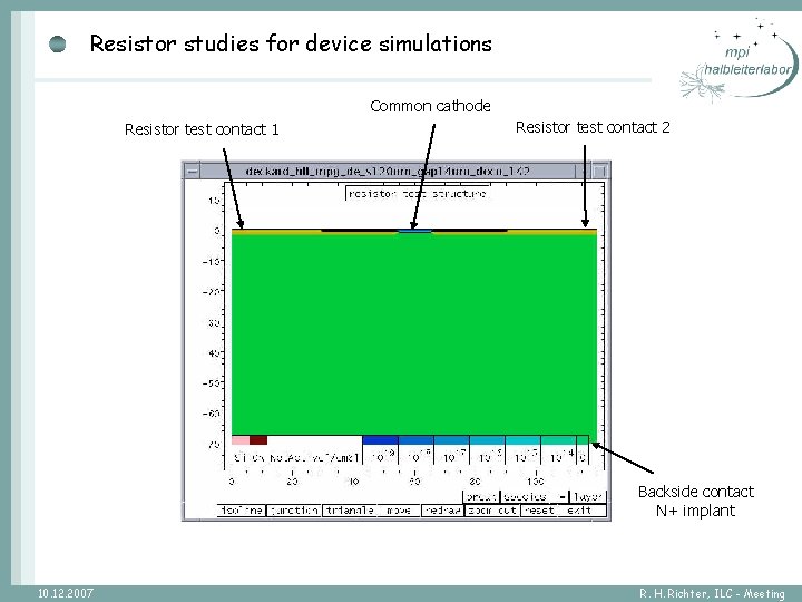
Resistor studies for device simulations Common cathode Resistor test contact 1 Resistor test contact 2 Backside contact N+ implant 10. 12. 2007 R. H. Richter, ILC - Meeting

Quench condition – parasitic JFET behavior Quench condition assuming p doped substrat Recovery times from 44 V -> 50 V (90%) NB: 2. 9 e 11 -> 1. 93 µs 3 e 12 -> 1. 72 µs 3. 1 e 12 -> 1. 55 µs lateral pinch off 20µA quench condition, (S. Cova et al, 1996) Deeper high field implantation ->diode capacitance reduction by a factor of 2 or 3 possible But recovery times by a factor 3 - 4 longer than with an optimum adjusted polysilicon resistor 10. 12. 2007 R. H. Richter, ILC - Meeting
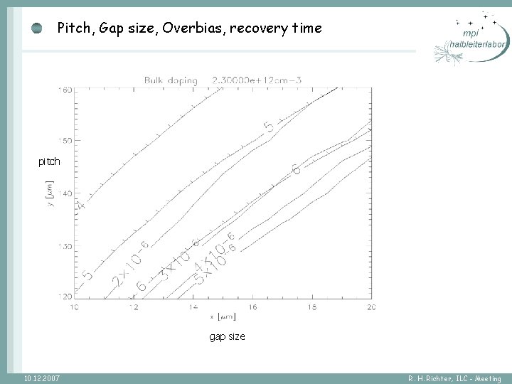
Pitch, Gap size, Overbias, recovery time pitch gap size 10. 12. 2007 R. H. Richter, ILC - Meeting

Pitch, Gap size, Overbias, recovery time Doping variation of 10% pitch gap size 10. 12. 2007 R. H. Richter, ILC - Meeting
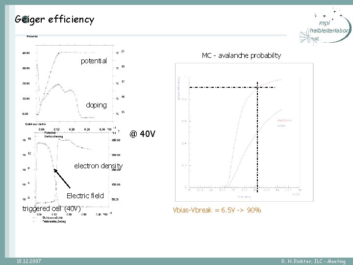
Geiger efficiency MC - avalanche probabilty potential doping @ 40 V electron density Electric field triggered cell (40 V) 10. 12. 2007 Vbias-Vbreak = 6. 5 V -> 90% R. H. Richter, ILC - Meeting
PDE (photodetection eff. ) estimation for blue light PDE = geometrical fill factor * Geiger eff. * QE(entrance window) Hexagonal design pitch 150µm, isolation gap 20µm geomatrical fill factor 75% Optical entrance window: same as for backside illimunated devices: 90% @400 nm Geiger efficiency : 90% Product 10. 12. 2007 PDE: 61% (depends strongly on gap size) R. H. Richter, ILC - Meeting

Cross talk – bulk contribution device simulation Highly doped high field region is a diffusion barrier for holes (p n = ni²) generation of 1000 e/h pairs in the bulk Less than 1 hole in the high field region 10. 12. 2007 R. H. Richter, ILC - Meeting
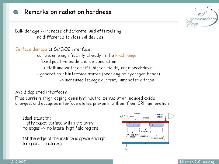
Remarks on radiation hardness Bulk damage -> increase of darkrate, and afterpulsing no difference to classical devices Surface damage at Si/Si. O 2 interface can become significantly already in the krad range - fixed positive oxide charge generation -> flatband voltage shift, higher fields, edge breakdown - generation of interface states (breaking of hydrogen bonds) -> increased leakage current, amphoteric traps Avoid depleted interfaces Free carriers (high doping densitys) neutralize radiation induced oxide charges, and occupies interface states preventing them from SRH generation Ideal situation: Highly doped surface within the array no edges -> no lateral high field regions (At the edge of the matrice is space enough for guard structures) 10. 12. 2007 R. H. Richter, ILC - Meeting

Pros and Cons Advantages: - no need of polysilicon (process complexity, minimum feature size, reliable resistance, obstacle for light, insulator breakdown problem) - free entrance window for light, no metal necessary within the array -> easy antireflective coating - coarse lihographic level - simple technology - inherent diffusion barrier against minorities in the bulk -> less optical cross talk? - hopefully good radiation hardness Drawbacks: - required depth for vertical resistors does not match wafer thickness wafer bonding is necessary - changes of subpixel size requires other material - vertical ‘resistor‘ is a JFET -> parabolic IV -> longer recovery times 10. 12. 2007 R. H. Richter, ILC - Meeting
Next steps Prototyping at MPI-HLL Proof of principle Ordered: 50 SOI wafer (150 mm), 70µm top wafer thickness, n-type, 1. 8 k. Ohmcm+/-70 Ohmcm at ICEMOS (Ireland), 400€/wafer Check reliability of specified wafer resistances Suitable for a subpixel size of about 125µm Minimum gap size? Optical crosstalk studies Processing: mask design ready Process technology with only 4 mask steps Processing until spring 08 If successful: technology transfer to an industrial partner is planned 10. 12. 2007 R. H. Richter, ILC - Meeting
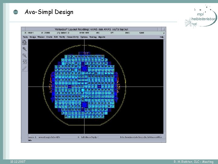
Ava-Simpl Design 10. 12. 2007 R. H. Richter, ILC - Meeting
Summary A silicon photomultiplier array with individual quench resistors, integrated into the silicon bulk is proposed. Wafer bonding technique provides the required flexibility for quench resistor adjustment replaces polysilicon and epitaxy Geometrical fill factor is given by the need of cross talk suppression only Very simple process, relaxed lithography requirements -> Cost reduction in mass production Pros and Cons see above Prototyping at HLL: Waiting for the SOI wafer Design is raedy. Samples available next spring. 10. 12. 2007 R. H. Richter, ILC - Meeting
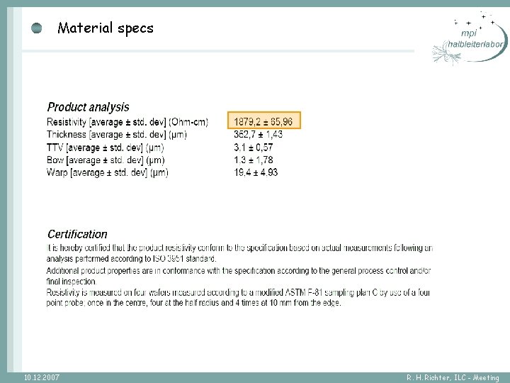
Material specs 10. 12. 2007 R. H. Richter, ILC - Meeting

Signal generation Anode discharge after trigger Fast signals are coupled by Cc 10. 12. 2007 R. H. Richter, ILC - Meeting
- Slides: 31