An Architecture for Reconfigurable Computing in Space Robert
An Architecture for Reconfigurable Computing in Space Robert F. Hodson 1, Kevin Somervill 1, John Williams 2, Neil Bergman 2, Rob Jones 3 1 NASA La. RC, 2 University of Queensland, 3 ASRC Aerospace RSC Hodson MAPLD 2005/130
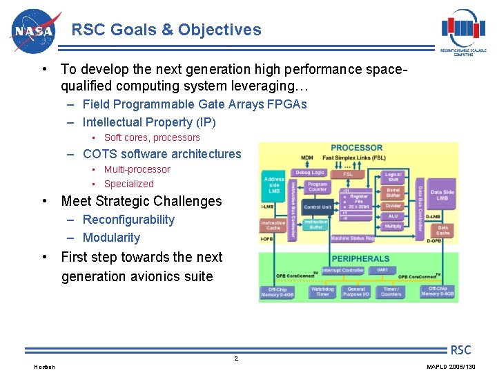
RSC Goals & Objectives • To develop the next generation high performance spacequalified computing system leveraging… – Field Programmable Gate Arrays FPGAs – Intellectual Property (IP) • Soft cores, processors – COTS software architectures • Multi-processor • Specialized • Meet Strategic Challenges – Reconfigurability – Modularity • First step towards the next generation avionics suite 2 Hodson RSC MAPLD 2005/130
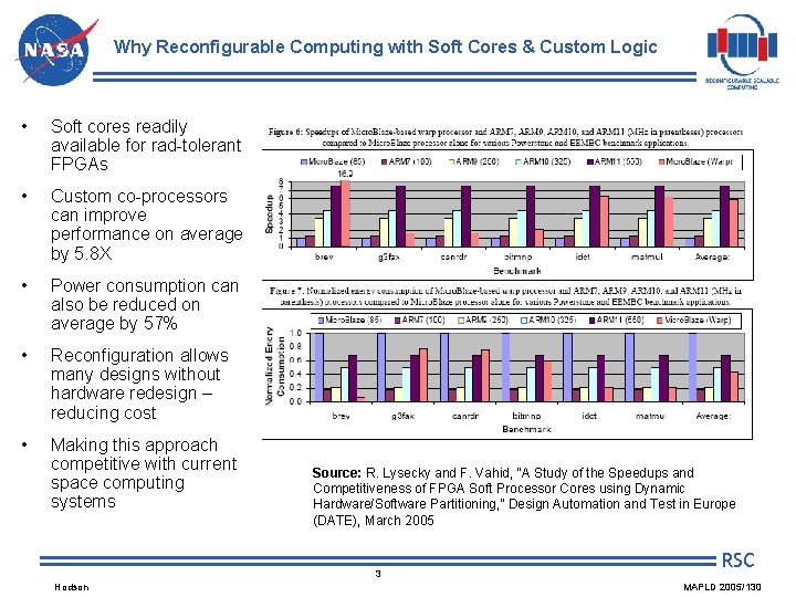
Why Reconfigurable Computing with Soft Cores & Custom Logic • Soft cores readily available for rad-tolerant FPGAs • Custom co-processors can improve performance on average by 5. 8 X • Power consumption can also be reduced on average by 57% • Reconfiguration allows many designs without hardware redesign – reducing cost • Making this approach competitive with current space computing systems Source: R. Lysecky and F. Vahid, “A Study of the Speedups and Competitiveness of FPGA Soft Processor Cores using Dynamic Hardware/Software Partitioning, ” Design Automation and Test in Europe (DATE), March 2005 3 Hodson RSC MAPLD 2005/130
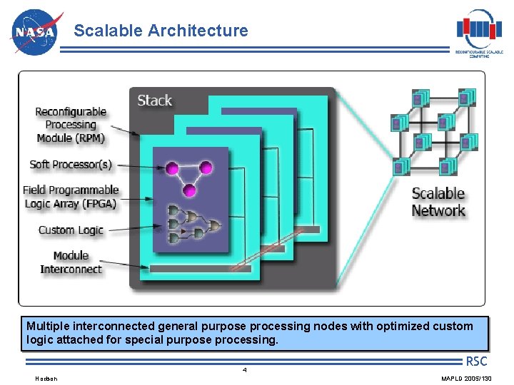
Scalable Architecture Multiple interconnected general purpose processing nodes with optimized custom logic attached for special purpose processing. 4 Hodson RSC MAPLD 2005/130
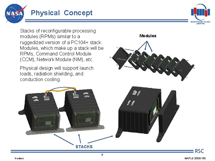
Physical Concept Stacks of reconfigurable processing modules (RPMs) similar to a ruggedized version of a PC 104+ stack. Modules, which make up a stack will be RPMs, Command Control Module (CCM), Network Module (NM), etc. Modules Physical design will support launch loads, radiation shielding, and conduction cooling. STACKS 5 Hodson RSC MAPLD 2005/130
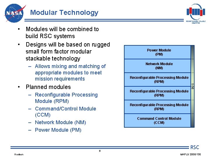
Modular Technology – Allows mixing and matching of appropriate modules to meet mission requirements • Planned modules Network Module (NM) Reconfigurable Processing Module (RPM) – Command/Control Module (CCM) – Network Module (NM) – Power Module (PM) Reconfigurable Processing Module (RPM) Command Control Module (CCM) 6 Hodson Power Module (PM) BUS • Modules will be combined to build RSC systems • Designs will be based on rugged small form factor modular stackable technology RSC MAPLD 2005/130
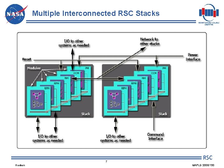
Multiple Interconnected RSC Stacks 7 Hodson RSC MAPLD 2005/130
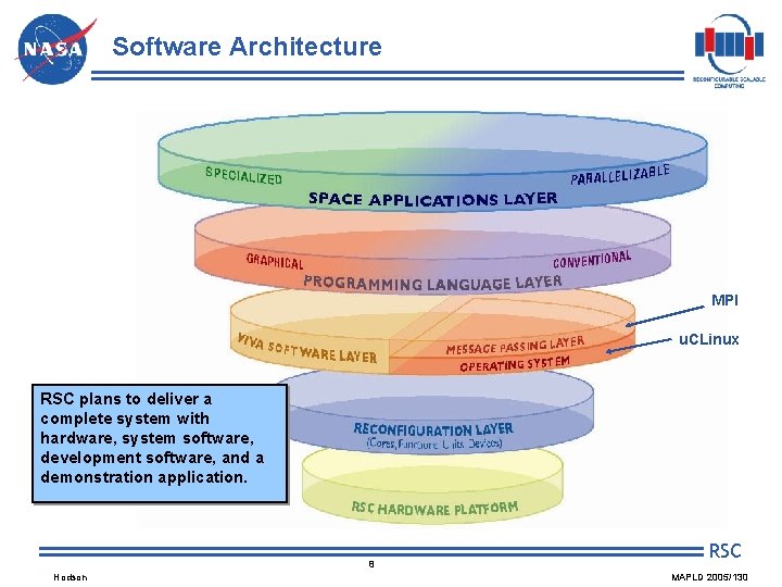
Software Architecture MPI u. CLinux RSC plans to deliver a complete system with hardware, system software, development software, and a demonstration application. 8 Hodson RSC MAPLD 2005/130
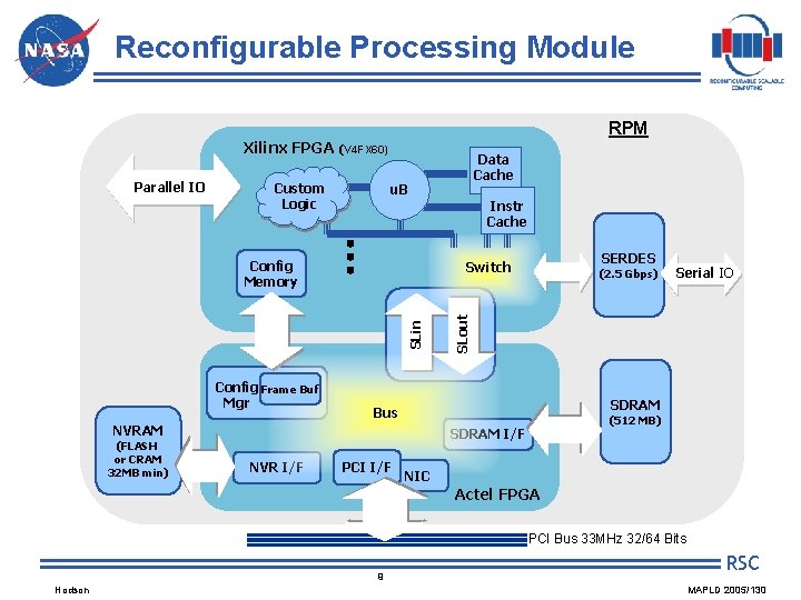
Reconfigurable Processing Module RPM Xilinx FPGA (V 4 FX 60) Custom Logic u. B Config Memory (2. 5 Gbps) (512 MB) SDRAM I/F NVR I/F PCI I/F Serial IO SDRAM Bus NVRAM (FLASH or CRAM 32 MB min) SERDES Switch SLin Config Frame Buf Mgr Instr Cache SLout Parallel IO Data Cache NIC Actel FPGA PCI Bus 33 MHz 32/64 Bits 9 Hodson RSC MAPLD 2005/130
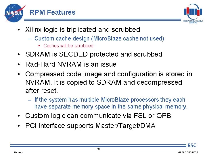
RPM Features • Xilinx logic is triplicated and scrubbed – Custom cache design (Micro. Blaze cache not used) • Caches will be scrubbed • SDRAM is SECDED protected and scrubbed. • Rad-Hard NVRAM is an issue • Compressed code image and configuration is stored in NVRAM. It is copied to SDRAM and decompressed after reset. – If the system has multiple Micro. Blaze processors they each have separate memory space in the same physical memory. • Custom logic can communicate via FSL or OPB • PCI interface supports Master/Target/DMA 10 Hodson RSC MAPLD 2005/130
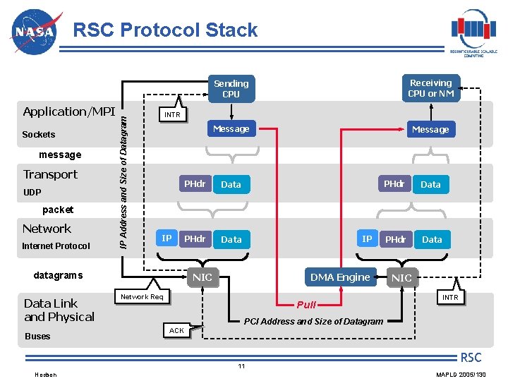
Application/MPI Sockets message Transport UDP packet Network Internet Protocol IP Address and Size of Datagram RSC Protocol Stack Buses Receiving CPU or NM Message INTR IP datagrams Data Link and Physical Sending CPU PHdr Data IP DMA Engine NIC Network Req Pull Data PHdr Data NIC INTR PCI Address and Size of Datagram ACK 11 Hodson PHdr RSC MAPLD 2005/130
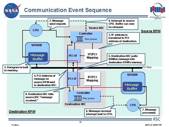
Communication Event Sequence 2. Message send request. Source NIC CPU Controller Req queue 9. Interrupt to source CPU. Buffer can now be released. Source RPM 3. IP address is translated to PCI address of destination. SDRAM Message Buffer IP 2 PCI Mapping PCI I/F 5. Destination NIC pulls (DMAs) message into destination RPM’s memory. PCI Bus 1. Datagram is built in memory. 4. PCI Address of message on source RPM sent to destination NIC. 8. Destination NIC tells source NIC “message received. ” IP 2 PCI Mapping PCI I/F Message Buffer Controller Req queue Destination NIC CPU 6. Message received interrupt sent to CPU. Destination RPM 12 Hodson SDRAM 7. Message processed. RSC MAPLD 2005/130
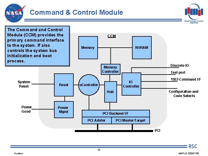
Command & Control Module The Command Control Module (CCM) provides the primary command interface to the system. If also controls the system bus initialization and boot process. CCM Memory NVRAM Discrete IO Memory Controller System Reset Test port 1553 Command I/F IO Controller u. Controller Configuration and Code Selects Hub Power Good Power Mgmt PCI Backend I/F PCI Arbiter PCI Master/Target PCI 13 Hodson RSC MAPLD 2005/130
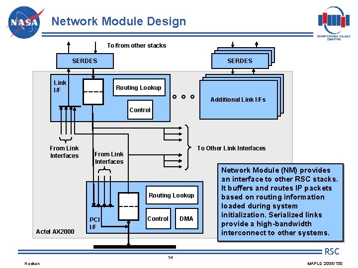
Network Module Design To/from other stacks SERDES Link I/F Routing Lookup Additional Link I/Fs Control From Link Interfaces To Other Link Interfaces From Link Interfaces Routing Lookup Actel AX 2000 PCI I/F Control 14 Hodson DMA Network Module (NM) provides an interface to other RSC stacks. It buffers and routes IP packets based on routing information loaded during system initialization. Serialized links provide a high-bandwidth interconnect to other systems. RSC MAPLD 2005/130
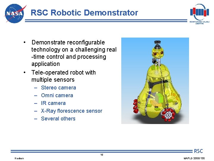
RSC Robotic Demonstrator • Demonstrate reconfigurable technology on a challenging real -time control and processing application • Tele-operated robot with multiple sensors – – – Stereo camera Omni camera IR camera X-Ray florescence sensor Several others 15 Hodson RSC MAPLD 2005/130
RSC Team • Core Team Members – NASA Langley Research Center (Lead) – NASA Goddard Space Flight Center – The University of Queensland – ARSC Aerospace – Jefferson Lab (Do. E) – Starbridge Systems – Department of Defense • Affiliate Members – Air Force Research Laboratory – SEAKR Engineering – Imagination Engines 16 Hodson RSC MAPLD 2005/130
- Slides: 16