An Algorithm for Optimal Decoupling Capacitor Sizing and

- Slides: 20

An Algorithm for Optimal Decoupling Capacitor Sizing and Placement for Standard Cell Layouts Haihua Su, Sani R. Nassif IBM ARL Sachin S. Sapatnekar ECE Department University of Minnesota 9/10/2021 ISPD'02, San Diego, CA 1

Outline l l l On-chip decap overview Modeling and noise analysis Problem formulation and Adjoint sensitivity analysis Decap sizing and placement scheme Experimental results Conclusion 9/10/2021 ISPD'02, San Diego, CA 2

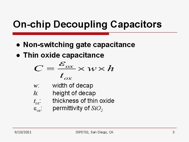
On-chip Decoupling Capacitors l l Non-switching gate capacitance Thin oxide capacitance w: h: tox: 9/10/2021 width of decap height of decap thickness of thin oxide permittivity of Si. O 2 ISPD'02, San Diego, CA 3

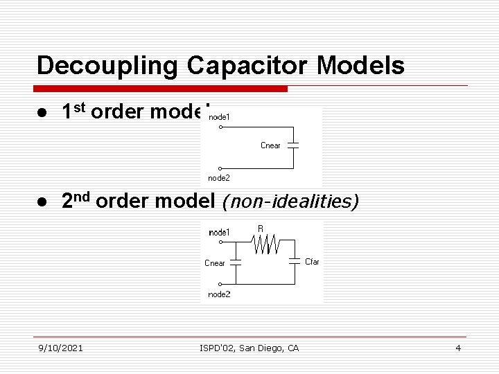
Decoupling Capacitor Models l 1 st order model l 2 nd order model (non-idealities) 9/10/2021 ISPD'02, San Diego, CA 4

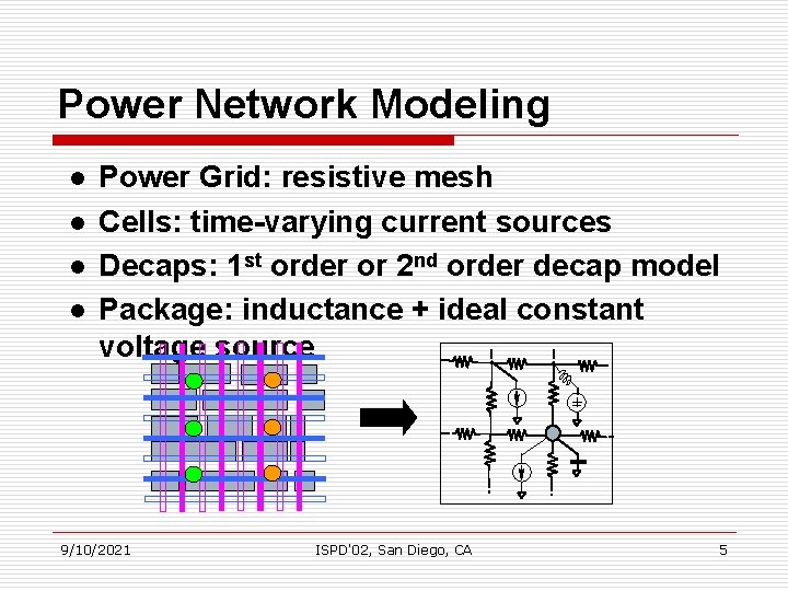
Power Network Modeling l l Power Grid: resistive mesh Cells: time-varying current sources Decaps: 1 st order or 2 nd order decap model Package: inductance + ideal constant voltage source + 9/10/2021 ISPD'02, San Diego, CA 5

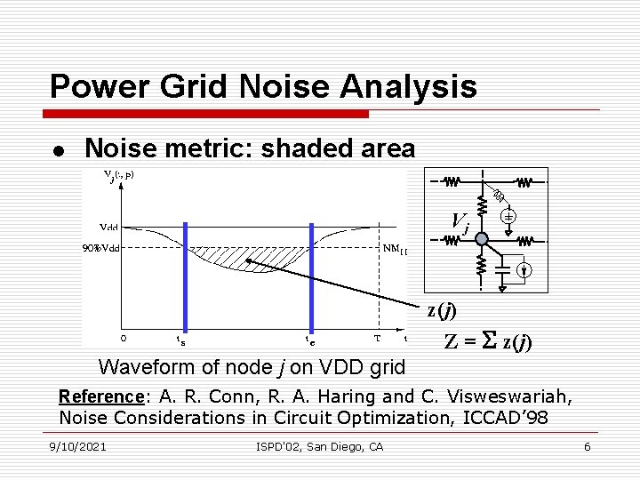
Power Grid Noise Analysis l Noise metric: shaded area Vj + z(j) Z = S z(j) Waveform of node j on VDD grid Reference: A. R. Conn, R. A. Haring and C. Visweswariah, Noise Considerations in Circuit Optimization, ICCAD’ 98 9/10/2021 ISPD'02, San Diego, CA 6

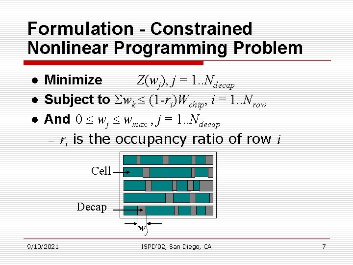
Formulation - Constrained Nonlinear Programming Problem l l l Minimize Z(wj), j = 1. . Ndecap Subject to Swk (1 -ri)Wchip, i = 1. . Nrow And 0 wj wmax , j = 1. . Ndecap – ri is the occupancy ratio of row i Cell Decap wj 9/10/2021 ISPD'02, San Diego, CA 7

Solver – Sequential Quadratic Programming (SQP) l l QPSOL - Quasi-Newton method to solve the problem of multidimensional minimization of functions with derivatives Requirements – – evaluation of the objective function and constraint functions calculation of first-order derivatives 9/10/2021 ISPD'02, San Diego, CA 8

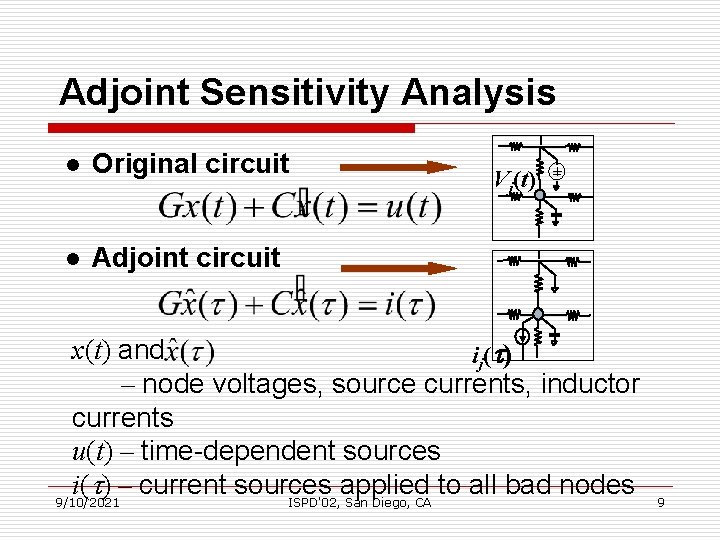
Adjoint Sensitivity Analysis l Original circuit l Adjoint circuit Vj(t) + x(t) and i j ( ) – node voltages, source currents, inductor currents u(t) – time-dependent sources i( ) – current sources applied to all bad nodes 9/10/2021 ISPD'02, San Diego, CA 9

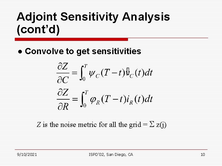
Adjoint Sensitivity Analysis (cont’d) l Convolve to get sensitivities Z is the noise metric for all the grid = S z(j) 9/10/2021 ISPD'02, San Diego, CA 10

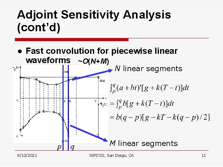
Adjoint Sensitivity Analysis (cont’d) l Fast convolution for piecewise linear waveforms ~O(N+M) N linear segments p 9/10/2021 q M linear segments ISPD'02, San Diego, CA 11

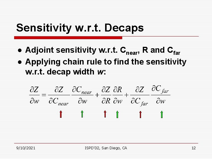
Sensitivity w. r. t. Decaps l l Adjoint sensitivity w. r. t. Cnear, R and Cfar Applying chain rule to find the sensitivity w. r. t. decap width w: 9/10/2021 ISPD'02, San Diego, CA 12

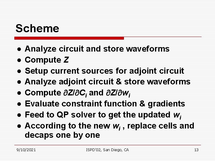
Scheme l l l l Analyze circuit and store waveforms Compute Z Setup current sources for adjoint circuit Analyze adjoint circuit & store waveforms Compute Z/ Ci and Z/ wi Evaluate constraint function & gradients Feed to QP solver to get the updated wi According to the new wi , replace cells and decaps one by one 9/10/2021 ISPD'02, San Diego, CA 13

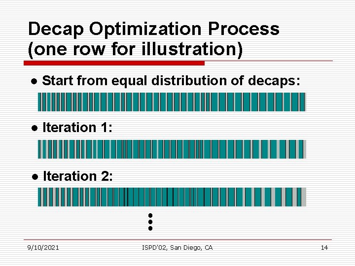
Decap Optimization Process (one row for illustration) l Start from equal distribution of decaps: l Iteration 1: l Iteration 2: 9/10/2021 ISPD'02, San Diego, CA 14

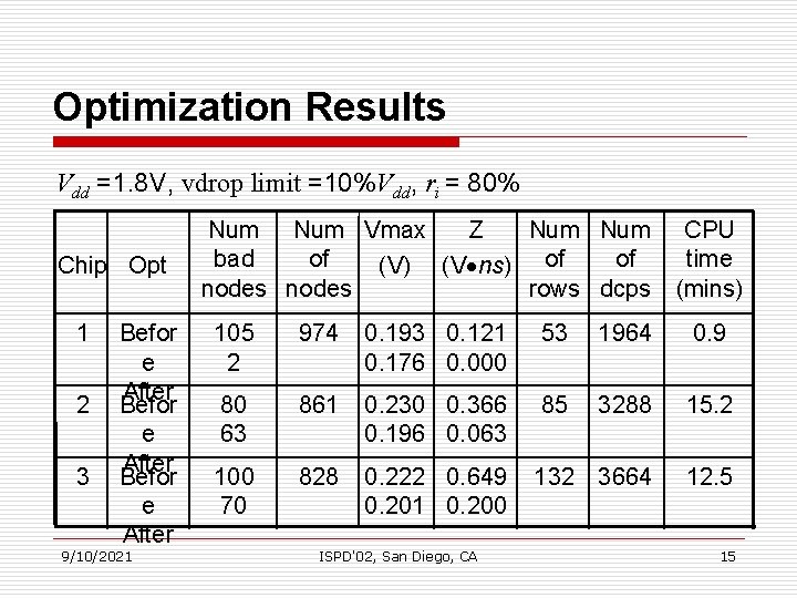
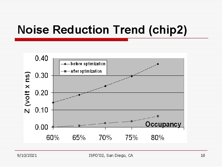
Optimization Results Vdd =1. 8 V, vdrop limit =10%Vdd, ri = 80% Chip Opt 1 2 3 Befor e After 9/10/2021 Num Vmax Z Num bad of of (V) (V ns) of nodes rows dcps CPU time (mins) 105 2 974 0. 193 0. 121 0. 176 0. 000 53 1964 0. 9 80 63 861 0. 230 0. 366 0. 196 0. 063 85 3288 15. 2 100 70 828 0. 222 0. 649 0. 201 0. 200 132 3664 12. 5 ISPD'02, San Diego, CA 15

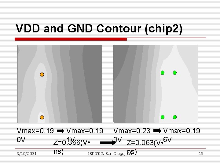
VDD and GND Contour (chip 2) Vmax=0. 19 1 V 0 V Z=0. 366(V • 9/10/2021 ns) Vmax=0. 19 Vmax=0. 23 0 V Z=0. 063(V • 6 V ns) ISPD'02, San Diego, CA 16

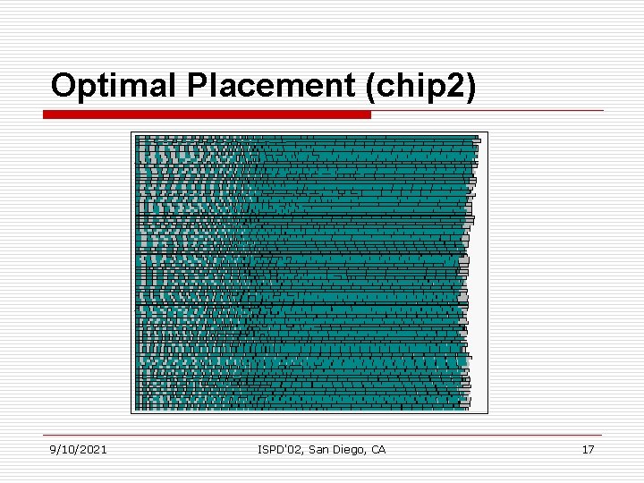
Optimal Placement (chip 2) 9/10/2021 ISPD'02, San Diego, CA 17

Noise Reduction Trend (chip 2) 9/10/2021 ISPD'02, San Diego, CA 18

Conclusion Proposed a scheme of decoupling capacitor sizing and placement for standard-cell layouts l Applied after placement and before signal routing l Formulated into nonlinear programming problem l Reduced transient noise l Presented a fast piece-wise linear waveform convolution for adjoint 9/10/2021 ISPD'02, San Diego, CA 19 sensitivity analysis l

Thank you! 9/10/2021 ISPD'02, San Diego, CA 20