Amplitude and Phase Noise in Nanoscale RF Circuits
![Jitter-Phase-Noise Relationships (1) • If all covariance terms are zero [Navid, 2005], PN (d. Jitter-Phase-Noise Relationships (1) • If all covariance terms are zero [Navid, 2005], PN (d.](https://slidetodoc.com/presentation_image_h/08595d0046fcbca998e7bf55ee2d2610/image-17.jpg)
![Phase Noise in Ring Oscillators (cont. ) • Using jitter-phase-noise relationships [Navid, 2005]: Dynamic Phase Noise in Ring Oscillators (cont. ) • Using jitter-phase-noise relationships [Navid, 2005]: Dynamic](https://slidetodoc.com/presentation_image_h/08595d0046fcbca998e7bf55ee2d2610/image-20.jpg)
- Slides: 31

Amplitude and Phase Noise in Nano-scale RF Circuits Reza Navid May 14, 2007

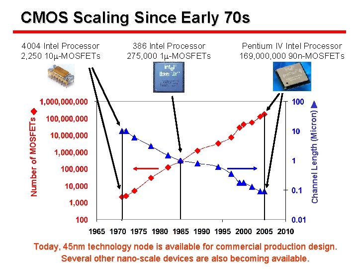
CMOS Scaling Since Early 70 s 386 Intel Processor 275, 000 1 m-MOSFETs Pentium IV Intel Processor 169, 000 90 n-MOSFETs Channel Length (Micron) Number of MOSFETs 4004 Intel Processor 2, 250 10 m-MOSFETs Today, 45 nm technology node is available for commercial production design. Several other nano-scale devices are also becoming available.

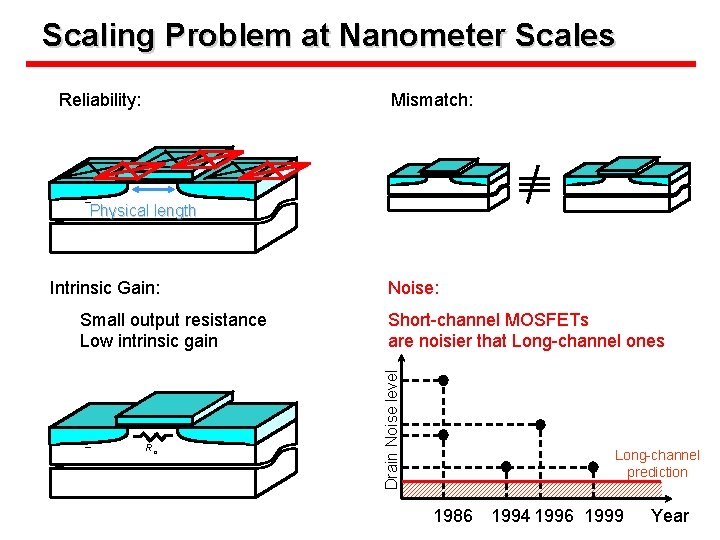
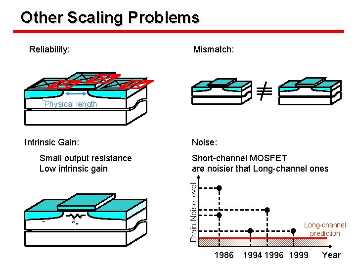
Scaling Problem at Nanometer Scales Reliability: Mismatch: Physical length Small output resistance Low intrinsic gain Ro Noise: Short-channel MOSFETs are noisier that Long-channel ones Drain Noise level Intrinsic Gain: Long-channel prediction 1986 1994 1996 1999 Year

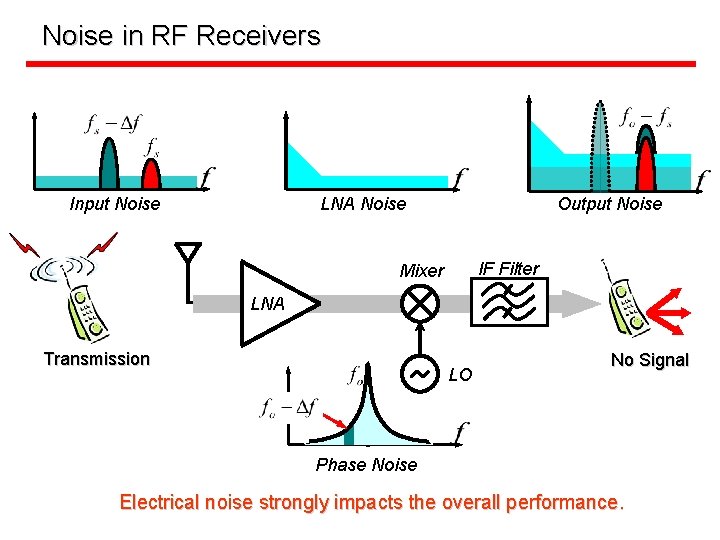
Noise in RF Receivers Input Noise LNA Noise Output Noise IF Filter Mixer LNA Transmission LO No Signal Phase Noise Electrical noise strongly impacts the overall performance.

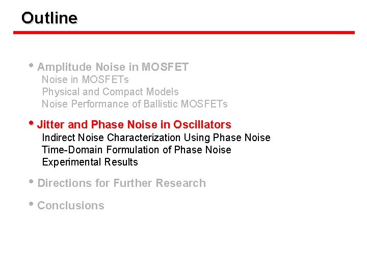
Outline • Amplitude Noise in MOSFETs Physical and Compact Models Noise Performance of Ballistic MOSFETs • Jitter and Phase Noise in Oscillators Indirect Noise Characterization Using Phase Noise Time-Domain Formulation of Phase Noise Experimental Results • Directions for Further Research • Conclusions

Outline • Amplitude Noise in MOSFETs Physical and Compact Models Noise Performance of Ballistic MOSFETs • Jitter and Phase Noise in Oscillators Indirect Noise Characterization Using Phase Noise Time-Domain Formulation of Phase Noise Experimental Results • Directions for Further Research • Conclusions

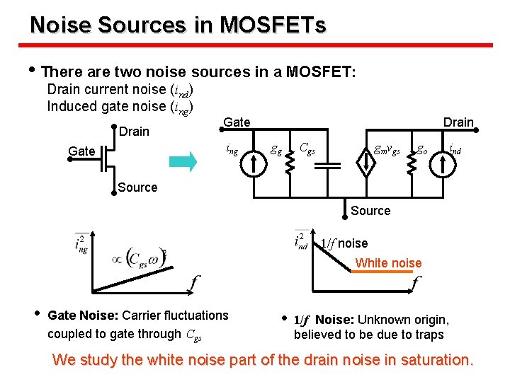
Noise Sources in MOSFETs • There are two noise sources in a MOSFET: Drain current noise (ind) Induced gate noise (ing) Drain Gate ing Gate Drain gg Cgs gmvgs go ind Source 1/f noise White noise • Gate Noise: Carrier fluctuations coupled to gate through Cgs • 1/f Noise: Unknown origin, believed to be due to traps We study the white noise part of the drain noise in saturation.

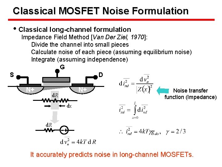
Classical MOSFET Noise Formulation • Classical long-channel formulation S Impedance Field Method [Van Der Ziel, 1970]: Divide the channel into small pieces Calculate noise of each piece (assuming equilibrium noise) Integrate (assuming independence) G D N+ N+ d. R Noise transfer function (Impedance) dx d. R It accurately predicts noise in long-channel MOSFETs.

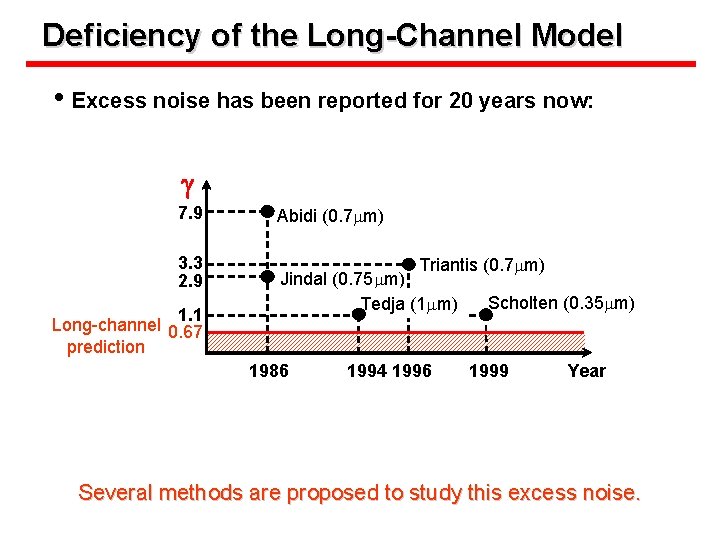
Deficiency of the Long-Channel Model • Excess noise has been reported for 20 years now: g 7. 9 3. 3 2. 9 1. 1 Long-channel 0. 67 prediction Abidi (0. 7 mm) Triantis (0. 7 mm) Jindal (0. 75 mm) Tedja (1 mm) 1986 1994 1996 Scholten (0. 35 mm) 1999 Year Several methods are proposed to study this excess noise.

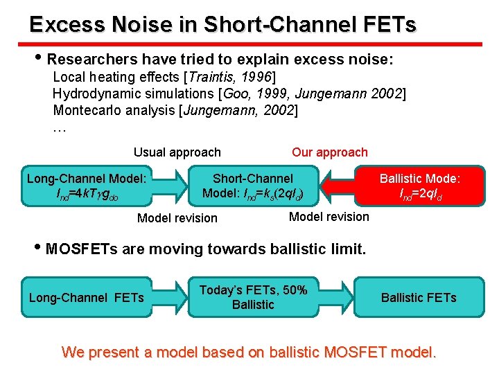
Excess Noise in Short-Channel FETs • Researchers have tried to explain excess noise: Local heating effects [Traintis, 1996] Hydrodynamic simulations [Goo, 1999, Jungemann 2002] Montecarlo analysis [Jungemann, 2002] … Usual approach Long-Channel Model: Ind=4 k. Tggdo Our approach Short-Channel Model: Ind=4 =kk. T Model: gshgd)do s(2 q. I Model revision Ballistic Mode: Ind=2 q. Id Model revision • MOSFETs are moving towards ballistic limit. Long-Channel FETs Today’s FETs, 50% Ballistic FETs We present a model based on ballistic MOSFET model.

Outline • Amplitude Noise in MOSFETs Physical and Compact Models Noise Performance of Ballistic MOSFETs • Jitter and Phase Noise in Oscillators Indirect Noise Characterization Using Phase Noise Time-Domain Formulation of Phase Noise Experimental Results • Directions for Further Research • Conclusions

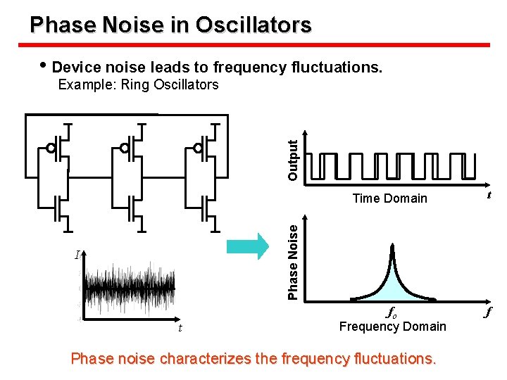
Phase Noise in Oscillators • Device noise leads to frequency fluctuations. Output Example: Ring Oscillators t fo Frequency Domain f Phase Noise Time Domain I t Phase noise characterizes the frequency fluctuations.

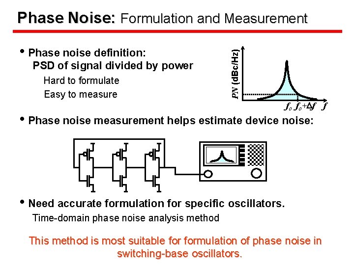
• Phase noise definition: PSD of signal divided by power Hard to formulate Easy to measure PN (d. Bc/Hz) Phase Noise: Formulation and Measurement fo fo+Df f • Phase noise measurement helps estimate device noise: • Need accurate formulation for specific oscillators. Time-domain phase noise analysis method This method is most suitable formulation of phase noise in switching-base oscillators.

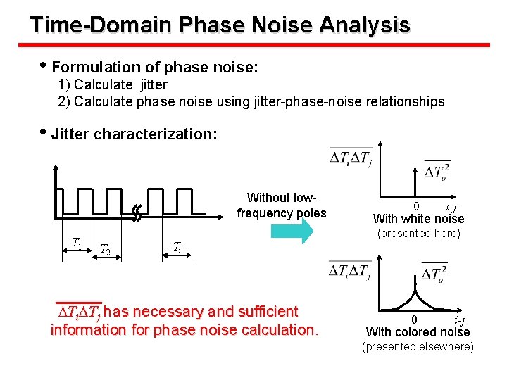
Time-Domain Phase Noise Analysis • Formulation of phase noise: 1) Calculate jitter 2) Calculate phase noise using jitter-phase-noise relationships • Jitter characterization: Without lowfrequency poles T 1 T 2 Ti DTi. DTj has necessary and sufficient information for phase noise calculation. 0 i-j With white noise (presented here) 0 i-j With colored noise (presented elsewhere)

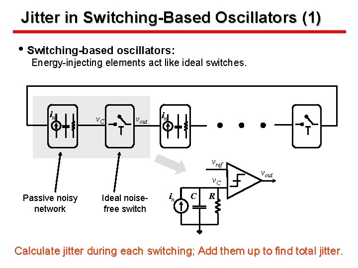
Jitter in Switching-Based Oscillators (1) • Switching-based oscillators: Energy-injecting elements act like ideal switches. in v. C vout in vref v. C Passive noisy network Ideal noisefree switch in C vout R Calculate jitter during each switching; Add them up to find total jitter.

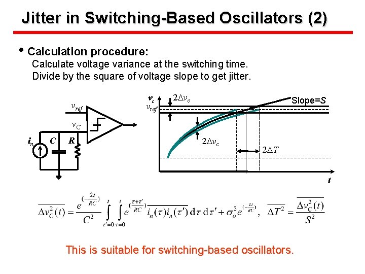
Jitter in Switching-Based Oscillators (2) • Calculation procedure: Calculate voltage variance at the switching time. Divide by the square of voltage slope to get jitter. vref vc vref 2 Dvc Slope=S v. C in C R 2 Dvc 2 DT t This is suitable for switching-based oscillators.
![JitterPhaseNoise Relationships 1 If all covariance terms are zero Navid 2005 PN d Jitter-Phase-Noise Relationships (1) • If all covariance terms are zero [Navid, 2005], PN (d.](https://slidetodoc.com/presentation_image_h/08595d0046fcbca998e7bf55ee2d2610/image-17.jpg)
Jitter-Phase-Noise Relationships (1) • If all covariance terms are zero [Navid, 2005], PN (d. Bc/Hz) Variance of one period Df (Hz) The 1 st harmonic The 3 rd harmonic Phase noise has peaks around odd harmonics, as expected.

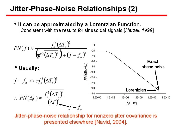
Jitter-Phase-Noise Relationships (2) • It can be approximated by a Lorentzian Function. Consistent with the results for sinusoidal signals [Herzel, 1999] PN(d. Bc/Hz) • Usually: Exact phase noise Lorentzian Df (Hz) Jitter-phase-noise relationship for nonzero jitter covariance is presented elsewhere [Navid, 2004].

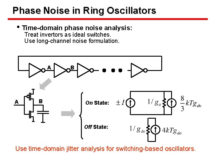
Phase Noise in Ring Oscillators • Time-domain phase noise analysis: Treat invertors as ideal switches. Use long-channel noise formulation. A A B B On State: Off State: Use time-domain jitter analysis for switching-based oscillators.
![Phase Noise in Ring Oscillators cont Using jitterphasenoise relationships Navid 2005 Dynamic Phase Noise in Ring Oscillators (cont. ) • Using jitter-phase-noise relationships [Navid, 2005]: Dynamic](https://slidetodoc.com/presentation_image_h/08595d0046fcbca998e7bf55ee2d2610/image-20.jpg)
Phase Noise in Ring Oscillators (cont. ) • Using jitter-phase-noise relationships [Navid, 2005]: Dynamic Power Very simple equations, but how accurate?

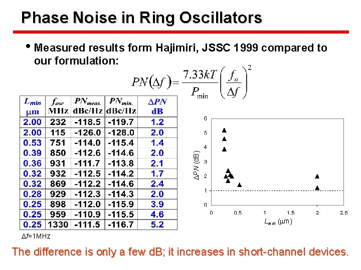
Phase Noise in Ring Oscillators • Measured results form Hajimiri, JSSC 1999 compared to DPN (d. B) our formulation: Lmin (mm) Df=1 MHz The difference is only a few d. B; it increases in short-channel devices.

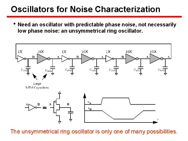
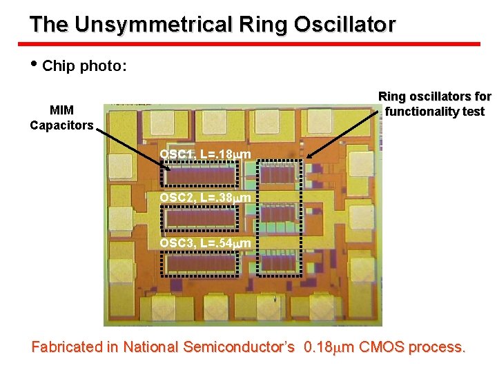
Oscillators for Noise Characterization • Need an oscillator with predictable phase noise, not necessarily low phase noise: an unsymmetrical ring oscillator. The unsymmetrical ring oscillator is only one of many possibilities.

The Unsymmetrical Ring Oscillator • Chip photo: Ring oscillators for functionality test MIM Capacitors OSC 1, L=. 18 mm OSC 2, L=. 38 mm OSC 3, L=. 54 mm Fabricated in National Semiconductor’s 0. 18 mm CMOS process.

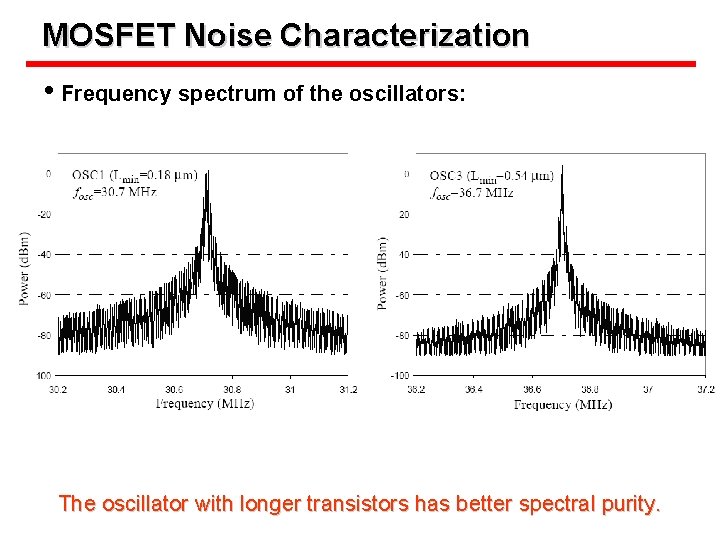
MOSFET Noise Characterization • Frequency spectrum of the oscillators: The oscillator with longer transistors has better spectral purity.

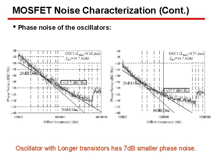
MOSFET Noise Characterization (Cont. ) • Phase noise of the oscillators: Oscillator with Longer transistors has 7 d. B smaller phase noise.

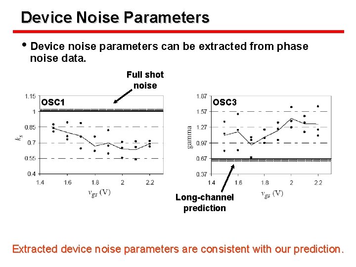
Device Noise Parameters • Device noise parameters can be extracted from phase noise data. Full shot noise OSC 1 OSC 3 Long-channel prediction Extracted device noise parameters are consistent with our prediction.

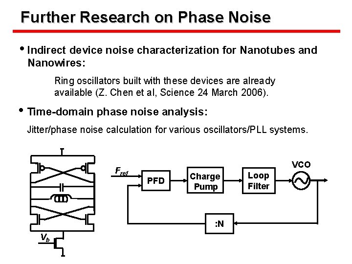
Further Research on Phase Noise • Indirect device noise characterization for Nanotubes and Nanowires: Ring oscillators built with these devices are already available (Z. Chen et al, Science 24 March 2006). • Time-domain phase noise analysis: Jitter/phase noise calculation for various oscillators/PLL systems. Fref VCO PFD Charge Pump : N Vb Loop Filter

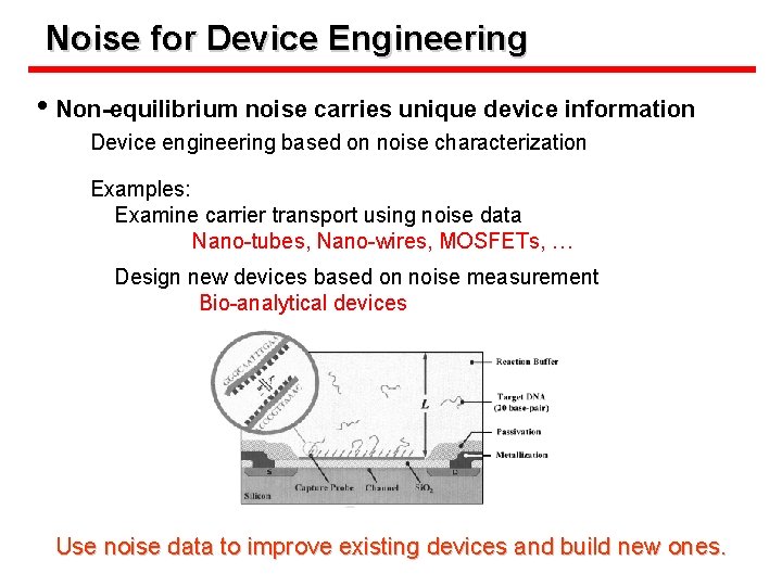
Noise for Device Engineering • Non-equilibrium noise carries unique device information Device engineering based on noise characterization Examples: Examine carrier transport using noise data Nano-tubes, Nano-wires, MOSFETs, … Design new devices based on noise measurement Bio-analytical devices Use noise data to improve existing devices and build new ones.

Other Scaling Problems Reliability: Mismatch: Physical length Small output resistance Low intrinsic gain Ro Noise: Short-channel MOSFET are noisier that Long-channel ones Drain Noise level Intrinsic Gain: Long-channel prediction 1986 1994 1996 1999 Year

Conclusions • Efficient CMOS analog design calls for a careful study of noise in MOSFETs, which has been a mystery for two decades. • Time domain phase noise analysis method accurately predicts the phase noise in switching-based oscillators. • Device noise can be characterized through phase noise measurement, facilitating process characterization. • Noise can be useful.

Acknowledgment This work is supported under an SRC customized research project from Texas Instruments and MARCO MSD center. We would like to thank National Semiconductor Inc. for the fabrication of test chips.