Amplifiers and their Frequency Response Instructor Engr Hira
- Slides: 15

Amplifiers and their Frequency Response Instructor: Engr. Hira Akash

Content • Cascade amplifier • The Amplifier pass band • The frequency plot • Low frequency plot • The un-bypassed emitter resistor • The Miller Effect Instructor: Engr. Hira Akash

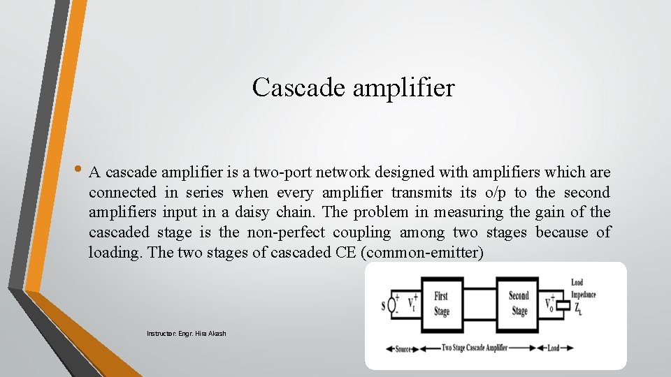
Cascade amplifier • A cascade amplifier is a two-port network designed with amplifiers which are connected in series when every amplifier transmits o/p to the second amplifiers input in a daisy chain. The problem in measuring the gain of the cascaded stage is the non-perfect coupling among two stages because of loading. The two stages of cascaded CE (common-emitter) Instructor: Engr. Hira Akash

Cont • • • This amplifier is used to enhance the strength of a signal in a TV receiver. In this amplifier, the primary stage of the amplifier can be connected to the secondary stage of the amplifier. To build a practical electronic system, a single-stage amplifier is not enough. Even though the amplifier’s gain mainly depends on parameters of the device as well as components of the circuit, there exists a higher limit of gain which can be attained from a single-stage amplifier. Therefore, the gain of this amplifier cannot be sufficient in practical application. To conquer this trouble, we require this amplifier’s two or more stages to amplify the overall amplifier’s voltage gain. As above one stage is used within series it is named as a multistage amplifier. The main drawback of the cascade amplifier is when several stages increases then the bandwidth will decrease. Instructor: Engr. Hira Akash

Applications of Cascade amplifier • This amplifier is used in tuned RF amplifiers within television circuits. • This amplifier can also be used as a wideband amplifier. • The isolation offered among input & output with these amplifiers is extremely high. Instructor: Engr. Hira Akash

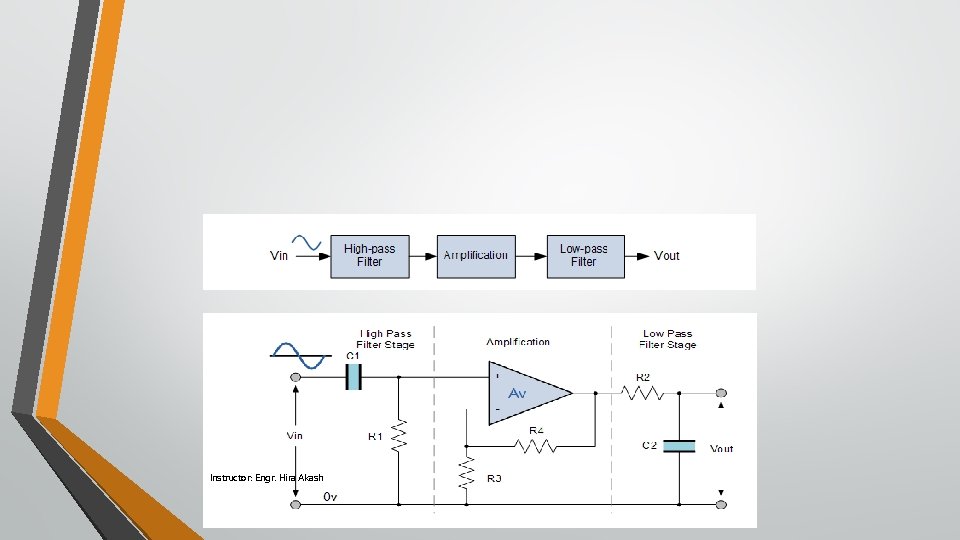
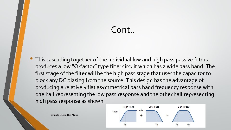
The Amplifier pass band • A band pass filter is an amplifier stage design to pass a range of frequencies while rejecting frequencies outside the upper and lower limits of the pass band. These filters can be made by combining the first order low pass and high pass filters. • The principal characteristic of a Band Pass Filter or any filter for that matter, is its ability to pass frequencies relatively unattenuated over a specified band or spread of frequencies called the “Pass Band”. Instructor: Engr. Hira Akash

Cont • For a low pass filter this pass band starts from 0 Hz or DC and continues up to the specified cut-off frequency point at -3 d. B down from the maximum pass band gain. Equally, for a high pass filter the pass band starts from this -3 d. B cut-off frequency and continues up to infinity or the maximum open loop gain for an active filter. Instructor: Engr. Hira Akash

Instructor: Engr. Hira Akash

Cont. . • This cascading together of the individual low and high passive filters produces a low “Q-factor” type filter circuit which has a wide pass band. The first stage of the filter will be the high pass stage that uses the capacitor to block any DC biasing from the source. This design has the advantage of producing a relatively flat asymmetrical pass band frequency response with one half representing the low pass response and the other half representing high pass response as shown. Instructor: Engr. Hira Akash

Frequency plot • • • A frequency plot is a graphical data analysis technique for summarizing the distributional information of a variable. The response variable is divided into equal sized intervals (or bins). The number of occurrences of the response variable is calculated for each bin. The frequency plot then consists of: Vertical axis = frequencies or relative frequencies; Horizontal axis = response variable (i. e. , the mid-point of each interval). There are 4 types of frequency plots: 1. frequency plot (absolute counts); 2. relative frequency plot (convert counts to proportions); Instructor: Engr. Hira Akash 3. cumulative frequency plot; 4. cumulative relative frequency plot.

Bypass resistor • A bypass capacitor is a capacitor that shorts AC signals to ground, so that any AC noise that may be present on a DC signal is removed, producing a much cleaner and pure DC signal. Instructor: Engr. Hira Akash

purpose of the Unbypassed emitter resistor • The unbypassed emitter resistor RE 1 serves three functions: 1. Adjust the voltage gain to a desired value: • When RE 1 = 0, the voltage gain of the amplifier is as high as it can be for the circuit at hand. • Setting RE 1 to a nonzero value provides a mechanism to decrease the gain to a desired value. Instructor: Engr. Hira Akash

What are the effects of an unbypassed emitter resistor? • • • In the emitter follower configuration, the emitter resistor is not bypassed and the output is taken off the emitter with unity gain and higher input impedance. In a common-emitter configuration, the output signal is taken off the collector that has a resistor to Vcc; and the emitter resistor is bypassed by a capacitor so that the emitter is at AC ground but has some DC bias. However, if the bypass capacitor is removed, there will be negative feedback to the base-emitter input signal and this should reduce the gain of the amplifier stage. A circuit designer could use resistors on both, the collector and the emitter, and take signals off both emitter and collector to feed the next stage of a tandem pair of PNP and NPN transistors. Instructor: Engr. Hira Akash

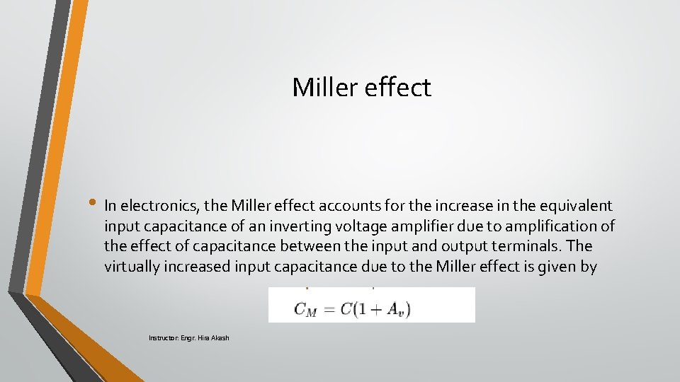
Miller effect • In electronics, the Miller effect accounts for the increase in the equivalent input capacitance of an inverting voltage amplifier due to amplification of the effect of capacitance between the input and output terminals. The virtually increased input capacitance due to the Miller effect is given by Instructor: Engr. Hira Akash

Miller effect • where -Av is the voltage gain of the inverting amplifier (Av positive) and C is the feedback capacitance • Although the term Miller effect normally refers to capacitance, any impedance connected between the input and another node exhibiting gain can modify the amplifier input impedance via this effect. These properties of the Miller effect are generalized in the Miller theorem. The Miller capacitance due to parasitic capacitance between the output and input of active devices like transistors and vacuum tubes is a major factor limiting their gain at high frequencies. Miller capacitance was identified in 1920 in triode vacuum tubes by John Milton Miller. Instructor: Engr. Hira Akash