AMICSA 2006 Magnetometer Frontend ASIC MFA Magnes W
![SNDR of HK-channel [d. B] MFA test results … TID example MFA 104 § SNDR of HK-channel [d. B] MFA test results … TID example MFA 104 §](https://slidetodoc.com/presentation_image_h2/42749e882fe9c81001ce90c2fdd9dbb2/image-14.jpg)

- Slides: 20

AMICSA 2006 Magnetometer Front-end ASIC (MFA) Magnes, W. 1), H. Hauer 2), A. Valavanoglou 1), M. Oberst 2), H. Neubauer 2), W. Baumjohann 1) and P. Falkner 3) Space Research Institute, Austrian Academy of Sciences, Graz, Austria 2) Fraunhofer, Institute for Integrated Circuits, Erlangen, Germany European Space Research and Technology Centre (ESA/ESTEC), Noordwijk, The Netherlands 1) 3) Xanthi, Greece, 3 rd Oct. 2006 1

Overview MFA… § Project goals § System level block diagram § Basic integration idea § Analog and digital realization § Test results of MFA 1 chip § Noise performance § Total ionization dose (TID) § Single event effects (SEE) § Temperature § Chip and instrument summary 2

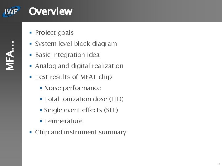
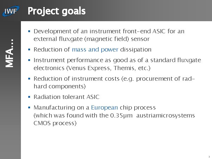
MFA… Project goals § Development of an instrument front-end ASIC for an external fluxgate (magnetic field) sensor § Reduction of mass and power dissipation § Instrument performance as good as of a standard fluxgate electronics (Venus Express, Themis, etc. ) § Reduction of instrument costs (e. g. procurement of radhard components) § Radiation tolerant ASIC § Manufacturing on a European chip process (which was found with the 0. 35µm austriamicrosystems CMOS process) 3

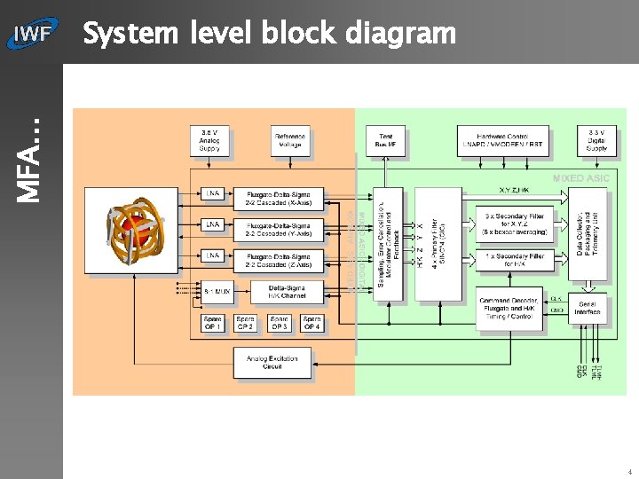
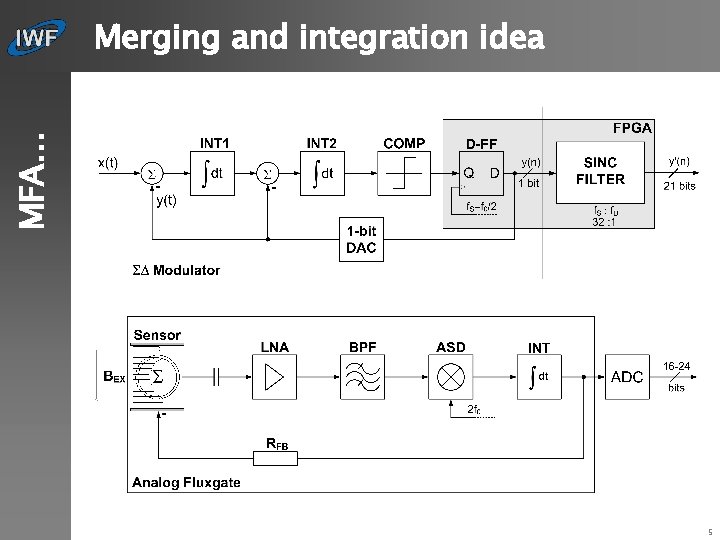
MFA… System level block diagram 4

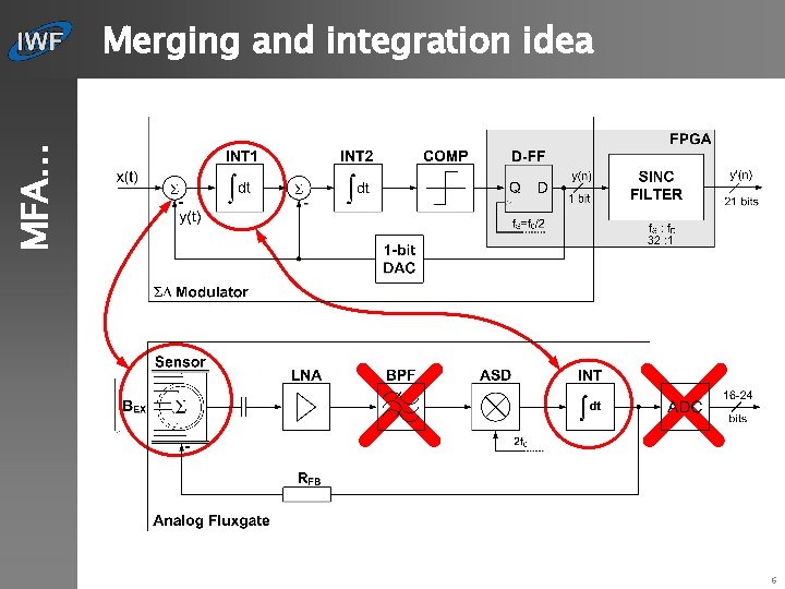
MFA… Merging and integration idea 5

MFA… Merging and integration idea 6

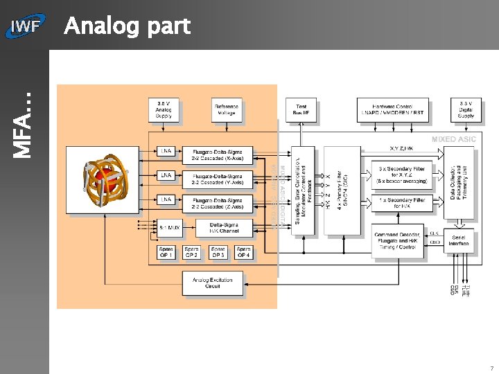
MFA… Analog part 7

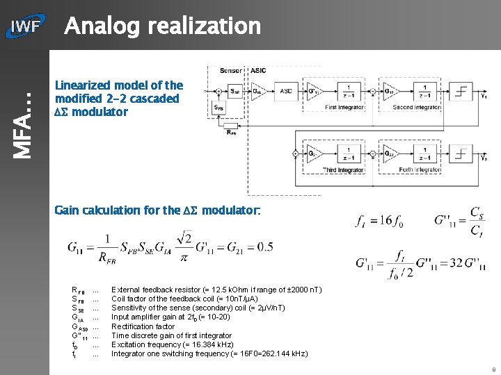
MFA… Analog realization Linearized model of the modified 2 -2 cascaded DS modulator Gain calculation for the DS modulator: RFB SSE GIA GASD G’’ 11 f 0 f. I … … … … External feedback resistor (= 12. 5 k. Ohm if range of ± 2000 n. T) Coil factor of the feedback coil (= 10 n. T/μA) Sensitivity of the sense (secondary) coil (= 2μV/n. T) Input amplifier gain at 2 f 0 (= 10 -20) Rectification factor Time discrete gain of first integrator Excitation frequency (= 16. 384 k. Hz) Integrator one switching frequency (= 16 F 0=262. 144 k. Hz) 8

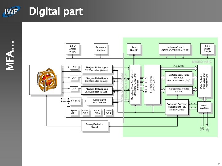
MFA… Digital part 9

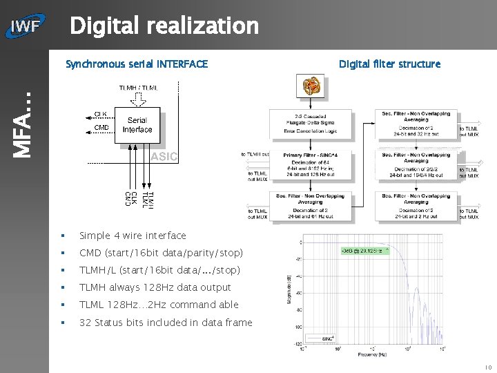
Digital realization Digital filter structure MFA… Synchronous serial INTERFACE § Simple 4 wire interface § CMD (start/16 bit data/parity/stop) § TLMH/L (start/16 bit data/. . . /stop) § TLMH always 128 Hz data output § TLML 128 Hz… 2 Hz command able § 32 Status bits included in data frame 10

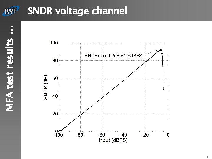
MFA test results … SNDR voltage channel 11

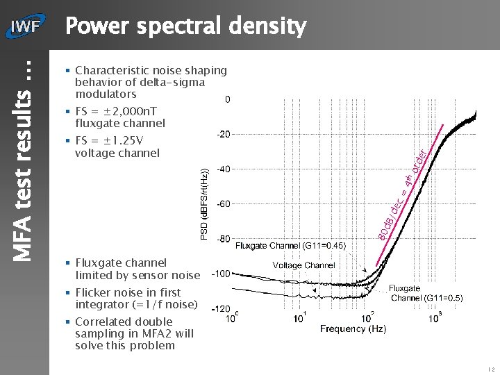
§ Characteristic noise shaping behavior of delta-sigma modulators § FS = ± 2, 000 n. T fluxgate channel /d ec = 4 t h ord er § FS = ± 1. 25 V voltage channel 80 d. B MFA test results … Power spectral density § Fluxgate channel limited by sensor noise § Flicker noise in first integrator (=1/f noise) § Correlated double sampling in MFA 2 will solve this problem 12

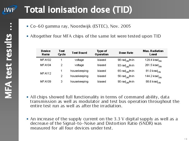
MFA test results … Total ionisation dose (TID) § Co-60 gamma ray, Noordwijk (ESTEC), Nov. 2005 § Altogether four MFA chips of the same lot were tested upon TID Device Name Test Cycle Test Board Type of Operation Dose Rate Max. Radiation Level MFA 102 1 voltage biased 98 rad(Si)/min 129. 4 krad(Si) MFA 104 2 voltage biased 93 rad(Si)/min 261. 5 krad(Si) 1 housekeeping biased 65 rad(Si)/min 81. 0 krad(Si) 2 housekeeping biased 56 rad(Si)/min 144. 2 krad(Si) 3 housekeeping biased 90 rad(Si)/min 88. 6 krad(Si) MFA 112 MFA 109 § All chips showed full functionality in terms of command ability, data transmission as well as modulator and test bus operation throughout the entire test run as well as after the irradiation. § An increase of the supply current on the 3. 3 V digital supply as well as a decrease of the Signal-to-Noise and Distortion Ratio (SNDR) was measured for all four devices under test. 13
![SNDR of HKchannel d B MFA test results TID example MFA 104 SNDR of HK-channel [d. B] MFA test results … TID example MFA 104 §](https://slidetodoc.com/presentation_image_h2/42749e882fe9c81001ce90c2fdd9dbb2/image-14.jpg)
SNDR of HK-channel [d. B] MFA test results … TID example MFA 104 § Test parameters: Dose rate: 93 rad(Si)/min; Total dose: 261. 5 krad(Si) § Current analog: constant at approx. 10 m. A § Current digital: increases 2. 55 m. A – 4. 13 m. A => +61% § SNDR: drops 72 d. B-62 d. B (4 -5 d. B per 100 krad) Missing data interpolated using linear interpolation Irradiation time [h] • red curve: PSD @ beginning; blue curve: PSD @ end • noise floor: increase 15 to about 65 μV/√Hz • fundamental sine 10 Hz and 30 Hz harmonics: unchanged • all the other harmonics: larger – increase as noise floor 14

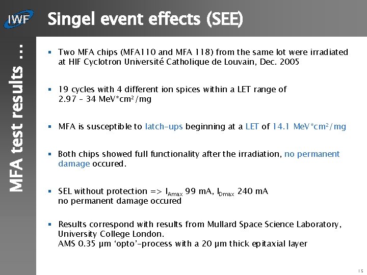
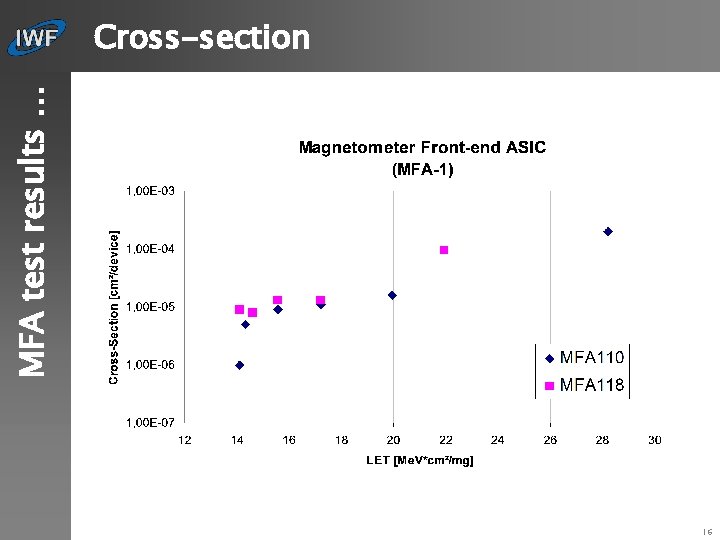
MFA test results … Singel event effects (SEE) § Two MFA chips (MFA 110 and MFA 118) from the same lot were irradiated at HIF Cyclotron Université Catholique de Louvain, Dec. 2005 § 19 cycles with 4 different ion spices within a LET range of 2. 97 – 34 Me. V*cm²/mg § MFA is susceptible to latch-ups beginning at a LET of 14. 1 Me. V*cm²/mg § Both chips showed full functionality after the irradiation, no permanent damage occured. § SEL without protection => IAmax 99 m. A, IDmax 240 m. A no permanent damage occured § Results correspond with results from Mullard Space Science Laboratory, University College London. AMS 0. 35 µm ‘opto’-process with a 20 µm thick epitaxial layer 15

MFA test results … Cross-section 16

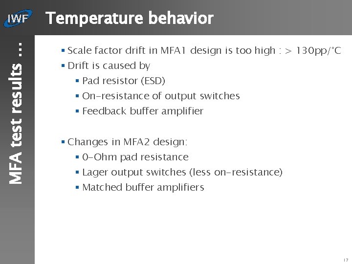
MFA test results … Temperature behavior § Scale factor drift in MFA 1 design is too high : > 130 pp/°C § Drift is caused by § Pad resistor (ESD) § On-resistance of output switches § Feedback buffer amplifier § Changes in MFA 2 design: § 0 -Ohm pad resistance § Lager output switches (less on-resistance) § Matched buffer amplifiers 17

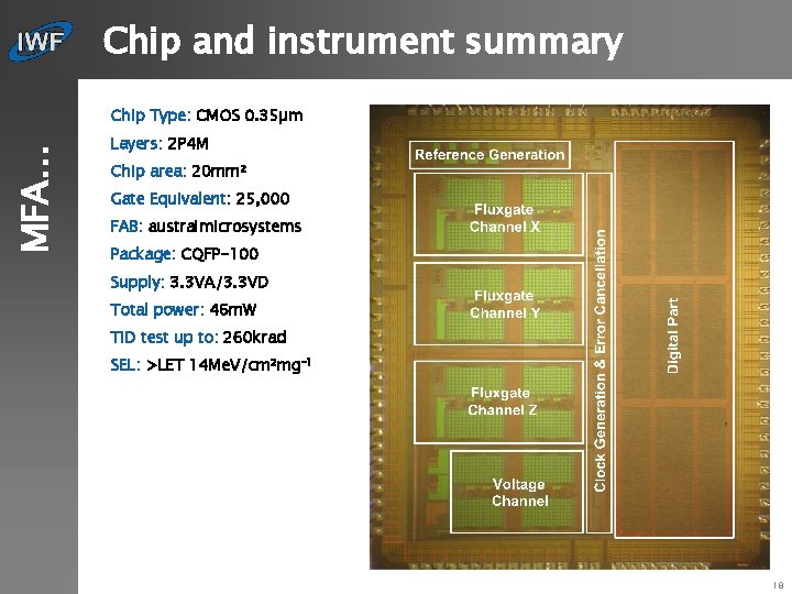
Chip and instrument summary MFA… Chip Type: CMOS 0. 35µm Layers: 2 P 4 M Chip area: 20 mm² Gate Equivalent: 25, 000 FAB: austraimicrosystems Package: CQFP-100 Supply: 3. 3 VA/3. 3 VD Total power: 46 m. W TID test up to: 260 krad SEL: >LET 14 Me. V/cm²mg-1 18

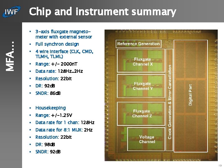
Chip and instrument summary MFA… § 3 -axis fluxgate magnetometer with external sensor § Full synchron design § 4 wire interface (CLK, CMD, TLMH, TLML) § Range: +/- 2000 n. T § Data rate: 128 Hz. . 2 Hz § Resolution: 22 bit § DR: 92 d. B § SNDR: 86 d. B § Housekeeping § Range: +/-1. 25 V § Data rate for 1 chan: 128 Hz § Data rate for 8: 1 MUX: 2 Hz § Resolution: 22 bit § DR: 98 d. B § SNDR: 92 d. B 19

Acknowledgements The authors would like to thank the European Space Agency Science Payload and Advanced Concepts Office for funding this project under contract no. 18391/04/NL/HB and, the Fraunhofer Institute for Integrated Circuits for the cooperation as sub-contractor for the chip integration and, the Institute of Meteorology and extraterrestrial Physics of the Technical University in Brunswick for supplying a highquality fluxgate sensor. 20