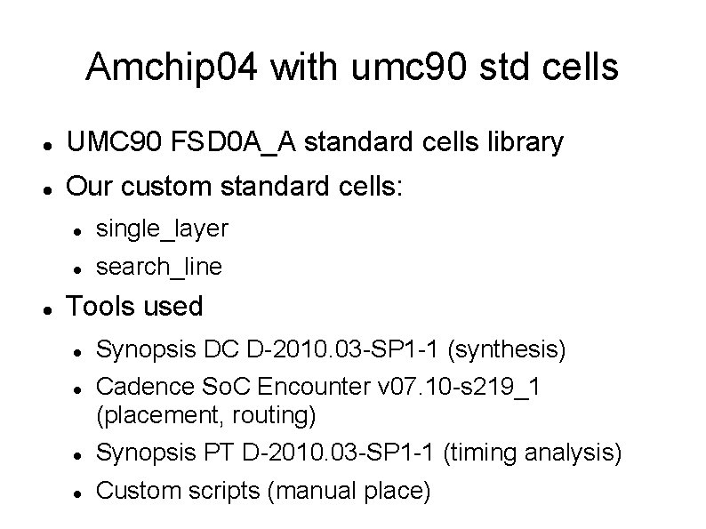
Amchip 04 with umc 90 std cells UMC
![CLK BL [15: 4] XXXXXX BL_N [15: 4] DATA ZZZZZZ XXXX slpre_t Mlpre_n BL CLK BL [15: 4] XXXXXX BL_N [15: 4] DATA ZZZZZZ XXXX slpre_t Mlpre_n BL](https://slidetodoc.com/presentation_image/2e5d661862bba90b9f601a7b17aa0cff/image-5.jpg)
![CLK BL [15: 4] XXXXXX BL_N [15: 4] Relative timing is critical! slpre_t Generated CLK BL [15: 4] XXXXXX BL_N [15: 4] Relative timing is critical! slpre_t Generated](https://slidetodoc.com/presentation_image/2e5d661862bba90b9f601a7b17aa0cff/image-6.jpg)
- Slides: 12

Amchip 04 with umc 90 std cells UMC 90 FSD 0 A_A standard cells library Our custom standard cells: single_layer search_line Tools used Synopsis DC D-2010. 03 -SP 1 -1 (synthesis) Cadence So. C Encounter v 07. 10 -s 219_1 (placement, routing) Synopsis PT D-2010. 03 -SP 1 -1 (timing analysis) Custom scripts (manual place)

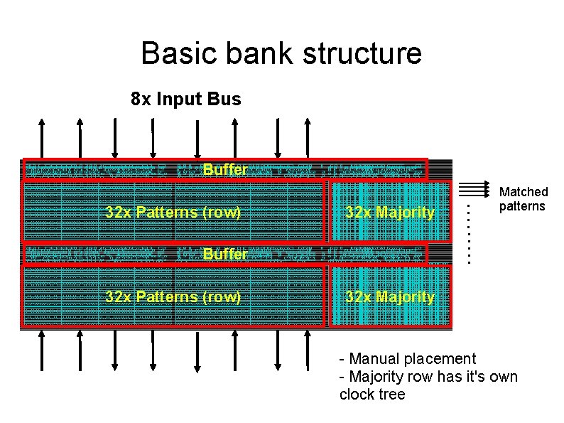
Basic bank structure 8 x Input Bus Buffer 32 x Majority Buffer 32 x Patterns (row) . . 32 x Patterns (row) Matched patterns 32 x Majority - Manual placement - Majority row has it's own clock tree

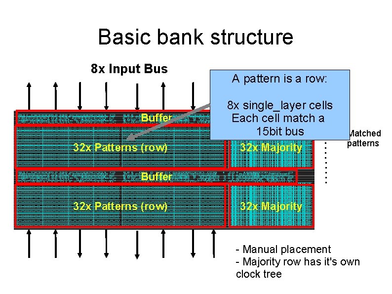
Basic bank structure 8 x Input Bus Buffer 8 x single_layer cells Each cell match a 15 bit bus 32 x Majority Buffer 32 x Patterns (row) . . 32 x Patterns (row) A pattern is a row: Matched patterns 32 x Majority - Manual placement - Majority row has it's own clock tree

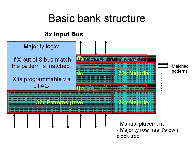
Basic bank structure 8 x Input Bus Majority logic: If X out of 8 bus match. Buffer the pattern is matched. 32 x Majority 32 x Patterns (row) 32 x Majority X is programmable via JTAG Buffer . . 32 x Patterns (row) Matched patterns - Manual placement - Majority row has it's own clock tree
![CLK BL 15 4 XXXXXX BLN 15 4 DATA ZZZZZZ XXXX slpret Mlpren BL CLK BL [15: 4] XXXXXX BL_N [15: 4] DATA ZZZZZZ XXXX slpre_t Mlpre_n BL](https://slidetodoc.com/presentation_image/2e5d661862bba90b9f601a7b17aa0cff/image-5.jpg)
CLK BL [15: 4] XXXXXX BL_N [15: 4] DATA ZZZZZZ XXXX slpre_t Mlpre_n BL [3: 0] BL_N [3: 0] XXXXXX Match Line MLSA_res SEN Match_reg DATA XXXX
![CLK BL 15 4 XXXXXX BLN 15 4 Relative timing is critical slpret Generated CLK BL [15: 4] XXXXXX BL_N [15: 4] Relative timing is critical! slpre_t Generated](https://slidetodoc.com/presentation_image/2e5d661862bba90b9f601a7b17aa0cff/image-6.jpg)
CLK BL [15: 4] XXXXXX BL_N [15: 4] Relative timing is critical! slpre_t Generated in each Buff module By global “read” signals Mlpre_n BL [3: 0] BL_N [3: 0] XXXXXX Match Line MLSA_res SEN Match_reg All this signals are inputs to the single_layer XXXX DATA ZZZZZZ pattern cell for activate the match. DATA XXXX

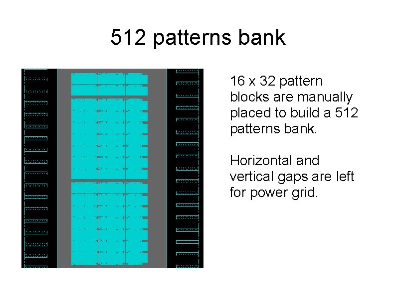
512 patterns bank 16 x 32 pattern blocks are manually placed to build a 512 patterns bank. Horizontal and vertical gaps are left for power grid.

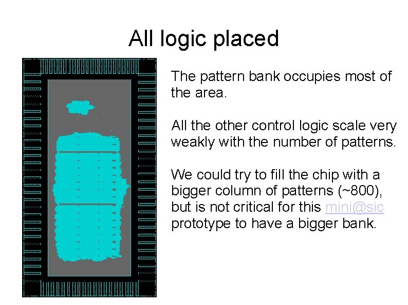
All logic placed The pattern bank occupies most of the area. All the other control logic scale very weakly with the number of patterns. We could try to fill the chip with a bigger column of patterns (~800), but is not critical for this mini@sic prototype to have a bigger bank.

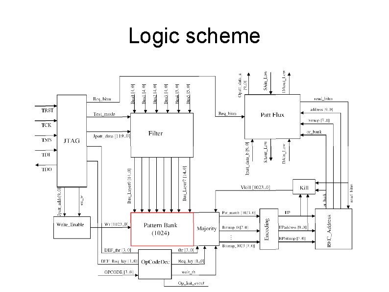
Logic scheme

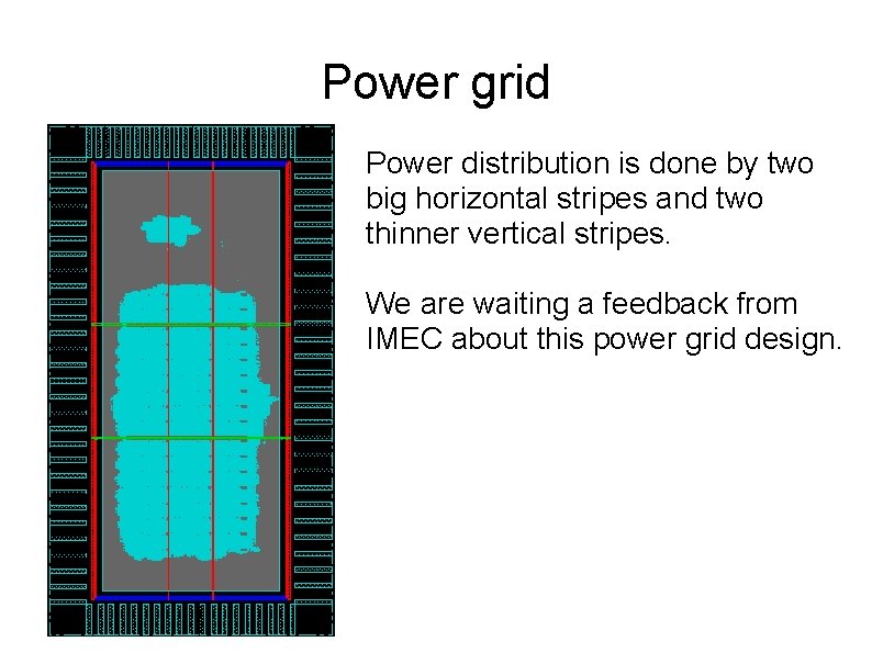
Power grid Power distribution is done by two big horizontal stripes and two thinner vertical stripes. We are waiting a feedback from IMEC about this power grid design.

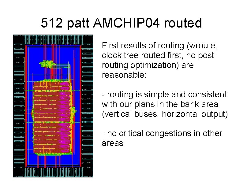
512 patt AMCHIP 04 routed First results of routing (wroute, clock tree routed first, no postrouting optimization) are reasonable: - routing is simple and consistent with our plans in the bank area (vertical buses, horizontal output) - no critical congestions in other areas

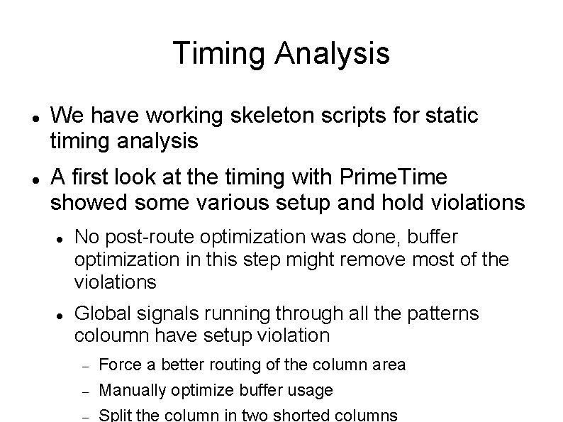
Timing Analysis We have working skeleton scripts for static timing analysis A first look at the timing with Prime. Time showed some various setup and hold violations No post-route optimization was done, buffer optimization in this step might remove most of the violations Global signals running through all the patterns coloumn have setup violation Force a better routing of the column area Manually optimize buffer usage Split the column in two shorted columns