AM chip schedule Alberto Adapt JTAG and bounday

AM chip schedule Alberto
 Design new CAM")
Adapt JTAG and bounday scan to MPW chip Design activities (17/11/2010) Design new CAM cells, Buffer logic New logic for kill? New logic majority PADs layout Opcode interface to new majority

Schedule/milestones • end of March: – a first version of the boundary scan is available – preliminary layout of the majority logic cell available – first version of the CAM-block available • starting beginning of April work on a first integration of the chip • end of April: after simulation and debugging… – a final version of the boundary scan is available – a complete layout of the majority logic cell – final design for the CAM-block available • starting beginning of May work on the final integration of the chip • end of May: successful integration of all pieces – during May test and simulation of the integrated design. • during June based on simulation decide what adjustments are needed • end of June: completed all simulations of the chip – the final and integrated chip should be completely simulated and approved. • early July submission

Majority interface component majority port ( CLK : in std_logic; INIT : in std_logic; REQ_LAY 0 : in std_logic; FORCE_READ : in std_logic; -- force read regardless of n-miss and layer 0 DISABLE_READ : in std_logic; MISS 0 : in std_logic; MISS 1 : in std_logic; MISS 2 : in std_logic; -- signals to write the DISABLE_THIS SRAM cell WL : in std_logic; DISABLE_THIS_SET : in std_logic; DISABLE_THIS_RESET : in std_logic; LAYER_MATCH : in std_logic_vector (7 downto 0); READ_FLAG : in std_logic; PATTERN_MATCH : out std_logic; ); end component;

Majority interface CLK Pattern_match INIT Read_flag layer_match<7. . 0> MISS 0 Global cfg signals, change just after clk rising edge layer_match<7. . 0> MISS 1 MISS 2 Require_layer 0 Force_read Disable_read Signals to write WL (write line) disable_this Disable_this_SET pattern Disable_this_RESET Fisher tree majority Layer_match is needed to output the map of fired layers.

Majority interface CLK Pattern_match INIT Read_flag WL layer_match<7. . 0> MISS 0 MISS 1 Global cfg signals, MISS 2 change just SET Require_layer 0 after clk Force_read rising edge Disable_read Signals to write WL (write line) disable_this Disable_this_SET pattern Disable_this_RESET Fisher tree layer_match<7. . 0> majority RESET Layer_match is needed to output the map of fired layers.

Where to put the Flip Flops? Majority logic & flag logic Match line bitline CAM cells 1 layer clk_N Sense Ampl. clk bitline Match enable ML reset ML MLSA Patt. match Bit line Propag. ML Match? Majority Propag. clk Layer-match SR latch Pattern match

Where to put the Flip Flops? Match enable Current source bitline clk_N Match line CAM cells 1 layer S R reset bitline Match enable reset ML Latch Bit line Propag. ML Match? Layer-match SR latch

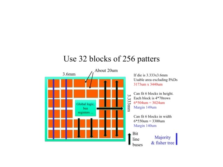
Use 16 blocks of 512 patters ? 3. 75 mm If die is 3. 2 x 3. 75 mm Usable area excluding PADs 3040 um x 3590 um 3. 2 mm Can fit 3 blocks in height 3*979 um = 2937 um Can almost fit 6 blocks in width 6*600 um = 3600 um Depends on block size! Can fit 3*5 blocks. Can fit 3*6 if block smaller than 600 um

Use 16 blocks of 512 patters ? 3. 75 mm If die is 3. 2 x 3. 75 mm Usable area excluding PADs 3040 um x 3590 um 3. 2 mm Can fit 3 blocks in height 3*979 um = 2937 um Can almost fit 6 blocks in width 6*600 um = 3600 um Depends on block size! Can fit 3*5 blocks. Can fit 3*6 if block smaller than 600 um

Block size April 7 th, 201 • Full custom block 64 x 4 (half of 64 patterns) – Width 225. 4 um * Height 122. 4 um (68 rows) • Pattern block of 64 patterns + buffer – Buffer 1 row ? – 8 layers width 450. 8 um no majority – Height with buffer 124. 2 um • • Height of 512 patterns = 993. 6 um Height of 3 x 512 patterns = 2980. 8 um 3. 2 mm – 160 um PADS – 2980. 8 um = 59. 2 um or 32 rows Max Pattern block width – (Chip 3. 75 mm – 160 um PADS)/6 = 3590 um / 6 = 598 um

AMchip 03 document • http: //agenda. infn. it/material. Display. py? con trib. Id=0&material. Id=0&conf. Id=3021

What we have now: Standard Cell 180 nm 5000 pattern/chip for 6 -layer patterns, 2500 pattern/chip for 12 -layer patterns “A VLSI Processor for Fast Track Finding Based on Content Addressable Memories”, IEEE Transactions on Nuclear Science, Volume 53, Issue 4, Part 2, Aug. 2006 Page(s): 2428 - 2433 65 nm technology provides a factor 8 → 20000 patterns/chip Full custom cell provides at least a factor 2 → 40000 patterns/chip 8 layers instead of 12 provides a factor 1, 5 → 60000 patterns/chip 1, 2 x 1, 2 cm^2 2 D chip → 80000 patterns/chip With a 2 D chip we gain a factor 30! NEXT: NEW 1 AMboard: 128 chips → ~10 Mpatterns per board VERSION 1 Crate: 16 AMboard → ~160 Mpatterns per crate For both L 1 & L 2 Current prototype under design: A. Annovi - ACES 2011 @ CERN 15 65 nm TSMC, 12 mm^2 MPW run, 100 MHz running clock

Pattern efficiency Pattern size r- : 24 pixels, 20 SCT strips z: 36 pixels Pattern size (half size) r- : 12 pixels, 10 SCT strips z: 36 pixels 90% 65 M 500 M # of patterns in Amchips (barrel only, 45 degress) Wa nt this <# roads/event @ 3 E 34> = 342 k <# roads/event @ 3 E 34> = 4 A. Annovi - ACES 2011 @ CERN 16

Variable resolution AM We can use don’t care on the least significant bit when we want to match the pattern layer @ r ns e r y e la patt carsercoarser resolution or use r e p 5 in s t i pattern all the bits to match it @ b of ” e ar ctor c t finer resolution ’ e fa n o finer patterns “d ctiv coarser 2 e th n eff i pattern W a n A. Annovi - ACES 2011 @ CERN D C gai • Patterns with 1 kid are stored at finer precision • Layers without “don’t care (DC)” can ignore 17 the hits in the

Goal: x 30 pattern density but lower power consumption 32 patterns of 8 layers ~ 60 mm x 500 mm ~ 1 or 2 pixels A. Annovi - ACES 2011 @ CERN 18
 • New CAM cells (Matteo,")
Tasks in Italy • New PADs layout (Stabile, Milano) • New CAM cells (Matteo, Frascati) – Complete NAND cell – Evaluate advantages of SRAM transistors – Other cells • Clean up project scripts (Francesco, Pisa) • Transition to 65 nm and new tools • Place and route (Francesco, Stabile)
 • JTAG logic to be looked at after Laura left •")
JTAG work (Germany) • JTAG logic to be looked at after Laura left • New features: – Add pins all MPW to boundary scan – Extend JPATT_DATA register to include as bit[0] a disable_pattern bit – Extend register for new busses (8 instead of 6)
 • Current draft from Jim is good and almost complete •")
Majority logic (Fermilab) • Current draft from Jim is good and almost complete • Features to be added: – Account for individual pattern disable – 4 thresholds: disable, 0 miss, 1 miss, 2 miss – Include option require_layer 0 • Layer 0 should be the closest to final AND • Design the basic majority logic cell
 • Transalate OPCODE output for new majority logic. 5 lines out:")
OPCODE work (Germany) • Transalate OPCODE output for new majority logic. 5 lines out: – Disable_match, 0 miss, 1 miss, 2 miss – require_layer 0 • Optional if time allows (coding and testing) – change input OPCODE protocol to single word
 • Optional if time allows (coding and testing) – Try a")
Kill tree (Fermilab) • Optional if time allows (coding and testing) – Try a new scheme for kill tree • Short description: – Current scheme encodes the highest priority pattern (encoder) – Then decodes it to set one kill FF – 1024 (or N patt) kill lines are then distributed to the patterns • Alternative: calculate kill along with priority encoder in a tree like fashion
 – All dates below are my")
Draft schedule • Aim for March submission (tight) – All dates below are my guess for discussion today • • NAND cell November NOR cell end of December NOR don’t care cell mid January (? ) Match line amplifier beginning of February – This item is late in the schedule • New PADs layout end of November – Important to check that all pads fit in a single MPW block • Project clean up and first place and route end of December • Preliminary version of majority mid December – Final end of January • New JTAG logic end of December: needed for 1 st place and route • New OPCODE and kill TREE end of January (mid Feb at latest)

Draft schedule during February • Put everything together • Final place and route • Prepare a detailed model of each CAM cell for mixed simulation of a few patterns. – Doing this in February is late, we should start it earlier, but currently uncovered • From now till the end: comparison of the implemented model with the C++ model for debugging. – Ilaria Sacco (Pisa) – This item is under staffed, we will need help here • Are we missing any important item? • First goal get Jim and Hans up and running – Please ask for needed information to start up
 q Why more dense")
Outline q The Pattern Matching and the Associative Memory (AM) q Why more dense AM we get better it is q Associative memory architecture q How chips are put together: Lamb → AMboard → crate q The Tree Search Processor & its location

TRACKING WITH PATTERN MATCHING The Event The Pattern Bank . . .

The Associative Memory – AM = Bingo • Dedicated device - maximum parallelism: • Each pattern with private comparator • Track search during detector readout Bingo scorecard • Full custom • FPGA • standard cell • new for FTK • 2 Tiers 700 350 180 90 65 65 nm: 0, 128 6 L nm: 5, 0 6 L nm: ~60 8 L nm: ~120 8 L nm 2, 5 D: 240 8 L kpat/chip kpat/chip

ONE PATTERN Layer 1 Cell 0 word FF Cell 2 FF Cell 3 word HIT FF word FF FF FF HIT FF Layer 4 HIT Output Bus Cell 1 Layer 3 Layer 2
 then")
Tracking in 2 steps: find Roads first (Pattern Matching with Associative Memory, AM) then find Tracks inside Road (Fit by TF) Hits Super Strip (SS) Hits Data Organizer (DO) Associative Memory (AM) Roads + hits Track fitting using full resolution of the detector Track Fitter (TF) Full Resolution Hits Large SS: Road a lot of fakes + combinatorics inside roads Road Hot point @high occupancy Tracks parameters (d, p. T, , h, z)

What we have now: Standard Cell 180 mm 5000 pattern/chip for 6 -layer patterns, 2500 pattern/chip for 12 -layer patterns “A VLSI Processor for Fast Track Finding Based on Content Addressable Memories”, IEEE Transactions on Nuclear Science, Volume 53, Issue 4, Part 2, Aug. 2006 Page(s): 2428 - 2433 90 nm technology provides a factor 4 → 10000 patterns/chip Full custom cell provides at least a factor 2 → 20000 patterns/chip NEXT: NEW VERSION For both L 1 & L 2 8 layers instead of 12 provides a factor 1, 5 → 30000 patterns/chip 1, 5 x 1, 5 cm**2 2 D chip → 60000 patterns/chip Going to 65 nm → 120000 patterns/chip With a 2 D chip we gain a factor 50! 1 AMboard: 128 chips → ~15 Mpatterns per board 1 Crate: 16 AMboard → ~245 Mpatterns per crate 100 MHz running clock
![Bus 3[17: 0] Bus 4[17: 0] Bus 5[17: 0] kill Add encoder Bus 1[17:](http://slidetodoc.com/presentation_image/c0f78f6844c64a2bf1b8948df89358ad/image-32.jpg "Bus 3[17: 0] Bus 4[17: 0] Bus 5[17: 0] kill Add encoder Bus 1[17:")
Bus 3[17: 0] Bus 4[17: 0] Bus 5[17: 0] kill Add encoder Bus 1[17: 0] Bus 2[17: 0] Pattern bank Bus 0[17: 0]

Power consumption Old Chip: corr. Factor 1, 8 Watt 180 nm 1, 8 V Core New chip 90 nm 1 V Core 1/(1, 8*1, 8) 0, 56 Watt Frequency 40 MHz New chip 100 MHz 100/40 1, 39 Watt Area 1 x 1 cm**2 New chip 4 cm**2 4/1 5, 56 Watt we would like to be 4 funding agencies involved: New: Pre-match feature 1/3 (1/2) Per crate 16 x 128 = 2048 chips 1, 85 (2, 78) Watt 3, 8 (5, 7) k. W IF the pre-match feature save at least 1/3, new 2 D chip (1, 85 W) ~ old chip (1, 8 W) ANY OTHER IDEA TO GAIN IN POWER INCREASES THE POTENTIALITY TO GROW IN THE THIRD DIRECTION

LHC Schedule 17, 6 pile-up ev. @2. 6 1033 19, 0 pile-up ev. @ 1034 Sim with 75 pile-up events after 2020! Concentrate now on 2013 -2015 (17 -19 pile-up events) Consider evolution up to 2019 (41, 5 pile-up events << simulated 75 ev) → Intermediate chip! 2020 comes much later and will profit of a very advanced technology……. Annovi, 27 -09 -2010 34

Our Schedule 1. 2. 3. 4. 5. 6. TSMC 65 nm, low power, available as mini@sic (Vcc_core=1, 2 V). 65 nm mini@sic 22, 5 k€/block; 90 nm mini@sic 18, 6 k€/block. "variable resolution" gives good results → early production of AM 04 we missed the 90 nm 2010 September run We propose to move directly to a 65 nm prototype. This is a preliminary schedule to produce new LAMBs for 2013: (1) Mini@sic submission: (2) delivery: (3) tested (4) MPW submission: (5) Delivery: (6) Tested: (7) MPW Production (8) Delivery (9) mounted on new Lambs spring or october 2011. ~february 2012 ~June 2012 from November 2012 from February 2013 from July 2013 from autumn 2013

Costs 2 blocks Mini@sic: payed by Italy MPW run: TSMC 2010: 12 mm^2 80 k. USD → 6, 7 k. USD/mm^2 UMC 2010: 4 mm x 4 mm 70 k€ → 4, 37 k € /mm^2 12 mm^2 ~ 1/8 AMchip 03 area in CDF → 7500 patterns/chip → 960 kpatterns/AMBoard With 2 blocks 160 k. USD → ~2 Mpatterns/AMBoard In 2012 could cost less – Academia Sinica can help on prize. Italy – Germany – USA – Academia Sinica (reduction). For 2013: small production = 8+2 AMBoards = 1280 chips. How many wafers? How much for a wafer? we would like to be 4 funding agencies, especially for final step: Whole wafer Mask @time when a large area chip is needed: UMC 2010 90 nm: 555 k. USD TSMC 2010 65 nm: 1300 -900 k. USD TSMC 2010 65 nm MLM 650 -950 k. USD

Pipelines of AM chips AMchip Control = GLUE add_in add_out

LAMB Bus 3 add_out Bus 1 AM Bus 4 Bus 2 INDI AMTOP add_in Bus 2 REV_EN Bus 4 Bus 5 Bus 0 AMBOTTOM Bus 5 PAT_ADD_OUT [17: 0] PAT_ADD_IN [17: 0] REV_EN Bus 3 add_out Bus 1
 INDI LAMB CONNECTORs FPGA")
GLUE AM VME INTERFACE ROAD CONNECTOR 6 bus (108 bits!) INDI LAMB CONNECTORs FPGA I/O control TRACKs PIPELINE REGISTERs FIFOS RECEIVERs & DRIVERs (ROAD bus + 6 HIT buses) HIT CONNECTOR Four 8 chips (topbottom) pipeline ADD OUT [30: 0] HIT [17: 0]

LAMB Standard cell chip Control FPGA 40 MHz clock FTK AMBoard Complementary Functions in the AUX board FPGA for Roads FPGA for SS Input 16 AMBoards per “core” crate → 8 core crates in the system P 3 serial LVDS CDF AMBoard with 4 LAMBs

LAMB Control FPGA 40 MHz clock Standard cell chip FPGA for SS Input Interface DO FPGA for Roads P 3 serial LVDS TF HW DO INPUT FIFOs Connectors for Hits LVDS Cables DO TF HW Connectors for tracks output AMBoard AUX card SSMAP Processing Unit DO+TF+HW DO TF HW CPU vme AM 15+…. . AM 14+…. . AM 13+…… AM 12+…. . 11 Lay. Fit+HW AM 11+…. . AM 9+…. . . AM 10+…. . AM 8+…. . 11 Lay. Fit+HW AM 7+TSP+DO+TF+HW AM 6+TSP+DO+TF+HW AM 5+TSP+DO+TF+HW AM 4+TSP+DO+TF+HW 11 Lay. Fit+ HW final AM 3+TSP+DO+TF+HW AM 2+TSP+DO+TF+HW AM 1+TSP+DO+TF+HW AM 0+TSP+DO+TF+HW 11 Lay. Fit+ HW final

The whole system: Data Formatter + 8 core crates Pixels & SCT RODs Data Formatter (DF) cluster finding split by layer 50~100 KHz event rate S-links overlap regions HITS 8 x h towers DO TF HW AM DO brd Core Crate AM brd TF HW Second stage Raw data ROBs Track data ROB ~Offline quality Track parameters
 Divide into sectors with overlaps")
1/2 AM IEEE Trans. Nucl. Sci. 51, 391 (2004) Divide into sectors with overlaps 6 18 -bit buses, hit rate: 40 MHz/bus input bandwidth of 4 Gbit/s 6 -12 Logical Layers: full h coverage Goal: High Lum 8 sectors • Pixel barrel SCT barrel Pixel disks 8 9 U VME crates for the FTK core Overlaps require hits in a small region to be sent to two neighboring AMs

Whatever is the power of the AM we can build, we can do better with the TSP
 PARENT PATTERN Depth 0 1")
FAT ROAD Found by AM (default SS for example) PARENT PATTERN Depth 0 1 5 2 6 3 7 4 8 Depth 1 PATTER N BLOCK Depth 2 Algorithm: NIM A 287 (1990) 436 -438 http: //www. pi. infn. it/~paola/Tree_search_algorithm. pdf Tree Search Processor: NIM A 287, 431 (1990), http: //www. pi. infn. it/~orso/ftk/NIMA 287_431. pdf IEEE Toronto, Canada, November 8 -14 1998 THIN ROAD 1 2 http: //www. pi. infn. it/~paola/TSP_v 14. pdf 3 4
 to be stored in AM or into a Mini-DO &")
Higher resolution SS (sub-ss) to be stored in AM or into a Mini-DO & LSB bits should be provided to TSP Example: 2 -Level TSP → divide by 4 each SS The AM chip for each found road could provide: 1) The Road IDentifier (address) 2) The Bitmap : one bit per layer, saying which SSs are empty & which are full (11 bits: 11101111111 eg. ) 3) 4 more bits for each layer, Sub-SS, saying which of the 4 SS subdivisions are empty and which are full (4 bits 8 Layers).

Conclusions Ø The application at future Instantaneus Luminosities will require AM extremely performing Ø Even if extremely performing, the AM work could be refined by the TSP that could fit in the same package with the AM chip in a 2. 5 D technology. This actually is NOT true any more, probably, before 2020 Ø The AM could be used for both L 1 and L 2 applications Ø Any AM pattern capacity increase would be an important advantage for both L 1 and L 2 tracking systems

BACKUP

New AMchip features Alberto Annovi INFN Frascati

Outline • • Use of patterns Variable size patterns New input busses Disabling patterns – Increase effective production yield Annovi, 27 -09 -2010 50

Pattern matching The Event The Pattern Bank . . . Annovi, 27 -09 -2010 51

Tracking in 2 steps 1. Find low resolution track candidates called “roads”. Solve most of the pattern recognition Roads Super Bin (SB) 2. Critical parameter: SS size Affects: Then fit tracks inside - Number of patterns for given efficiency: cost roads. - Number of found roads: workload for next step Thanks to 1 st step it is much easier Tracking with Annovi, 27 -09 -2010 ~offline quality 52

Pattern efficiency Pattern size r- : 24 pixel, 20 SCT 36 pix z Pattern size r- : 12 pixel, 10 SCT 36 pix z 90% 65 M 500 M # of patterns in Amchips (barrel only, 45 degress) Wa nt this <# roads/event @ 3 E 34> = 342 k <# roads/event @ 3 E 34> = 4 Annovi, 27 -09 -2010 53

Efficiency curve Need many patterns for little efficiency ? ? Super Bins are discr Edge effects give lots of patterns with little coverag # of pattern in Amchips (barrel only, 45 degress) Annovi, 27 -09 -2010 54

TSP simulation & varying-resolution pattern banks Guido Volpi & Roberto Vitillo FAT RO - Pisa We do have now a structured Depth 0 “pattern bank”, where each thin road is connected to its parent Depth 1 pattern in FTKsim. AM resolution Ongoing tests for TSP algo after TSP resolution the Road. Finder (AMsim) in Depth 2 FTKsim; AM Fake road is a AM matched pattern whose kids do not match th Thin ROAD we have studied the bank High probability to fire composition and. Low. AM FAKE probability AM patterns roads. to fire AM (symmetric): patterns: few kids many kids (up to 20 or (1 or 2): big more): no advantage to match it at TSP HIGH coverage match it at TSP resolution! More than LOW coverage patterns Annovi, 27 -09 -2010 55 resolution! All one kid can fire @ TSP patterns PARENT PATTERN KID PATTERN @Depth 0 PARENT @Depth 1

How to implement “variable resolution” in the AMchip We can use don’t care on the least significant bit when we want to match the pattern layer @ AM AM & TSP Pattern Bank for 23 resolution or use all the AM pattern distribution vs Num bits to match it @ TSP Majority of patterns with a sing resolution Test of AM patterns: 1. all single kid patterns @ TSP resolution AM resolution 2. For all few kid patterns use don’t (don’t care) care only for layers where both Half -SS are used by kids WH @1034 TSP resolution (care) to exclude the right half in these layers Annovi, 27 -09 -2010 Fake AM roads Guido Volpi & Roberto Vitillo # of kids - Pisa # of kids All AM roads with at least 1 matched kid 56

AM with care/don’t care <roads/event > TSP 38000 AM@TSP 28000 AM@DC 44000 AM 342000 Annovi, 27 -09 -2010 # of kids Care/don’t care very effective to reduce the numb Area cost on the chip approx. 1 extra cell for each Now 15 cells/layers. With 1 DC bit area increases by 1/15 ~ 7%. For comparison going to TSP resolution would req 57

Number of busses • • • Currently we have 6 input busses New AMchip should handle 8 layers IBL will require 2 busses for higher b/w External SCT layers needs half b/w Current package constraint max 7 input busses 3 options: implement 2 of them to be selected online Annovi, 27 -09 -2010 58
 Pattern bank with 8 matching layers 8")
8 Layers vs 7 buses (option 1) Pattern bank with 8 matching layers 8 internal buses Internal register that feeds 8 busses Demultiplex based on MSB Ex P tra i x P P i i x X Annovi, 27 -09 -2010 S S SCT C C 2&3 T T Input register for 7 busses 59

IBL: 7 Layers vs 7 buses Special IBL layer: OR of 2 layers I I B B Annovi, 27 -09 -2010 L L IBL @ double bandwidth. Either double internal clock, or special logic. P i x Take the logical OR of 2 layers. Both layers store the IBL super bin. Distribute 50% data to each Internal register that feeds 8 busses layer. Demultiplex based on MSB Layer matches if any of 2 IBL SCT layers match Input register for 7 busses P S S i C C 2&3 X T T 60

IBL: 8 Layers vs 7 buses IBL with double clock IBL @ double bandwidth. Either double internal clock, or special logic. I I B B Annovi, 27 -09 -2010 L L P i x P ? i ? X ? Take the logical OR of 2 layers. Both layers store the IBL super bin. Distribute 50% data to each Internal register that feeds 8 busses layer. Demultiplex based on MSB Layer matches if any of 2 IBL SCT layers match Input register for 7 busses S C 2&3 T 61

Amchip 03 yields • AMchip 03 prototype 2004 – 1 cm^2 MPW yield 35% • AMchip 03 production 2005 – 1 cm^2 pilot run yield 70% • Large fraction of failures due to single pattern defect. • Add one register to disable bad patters – Will allow to use all chips with a single (or few) pattern defects. • Area cost small : 1 flip-flop/pattern (not /layer) Annovi, 27 -09 -2010 62

Changes to AMChip specifications • Amchip 03 specs: – http: //wwwcdf. fnal. gov/publications/cdf 7339_amchip 03_s pecs. ps • New features – Add 1 or 2 don’t care bits/layer – Increase input busses to 7 with multiplexing & special handling of IBL – Add disable FF for each pattern Annovi, 27 -09 -2010 63

BACKUP Annovi, 27 -09 -2010 64

Two possible Approaches to expand into the third direction VIPRAM - Vertically Integrated Pattern Recognition Associative Memory Ted/Jim/Aida/Ray/Gregory/Simon/Silvia/Marcel/Gary/Mel/Bob… FNAL/ANL/UC/Tezzaron/… 1. “Identical Tier” 3 D architecture (actually 2. 5 D? ) 2. “True 3 D” Implementation

Trying to define a collaboration Italy-USA for DOE application to Generic R&D funds (ATLAS FTK - Fermilab CMS, both interested)

All equal tiers: put them in pipeline as done on the board

The 3 D IO Wrapper must be designed and fabricated around the 2 D AMchip to ensure that all tiers act as a single chip as shown in Figure 5. Even for prototyping purpose, it is not possible to simply take an existing, fabricated AMchip and place it inside a rectangular doughnutshaped 3 D IO Wrapper. There are several ways to address this. • First, the 2 D AMchip could be redesigned in a 3 D process like Tezzaron/Chartered, and then the 3 D IO Wrapper could be designed around it. This method has no obstacles to its 3 D fabrication. However, it does require the redesign of the AMchip. • Second, the CMOS UMC process could be used for 3 D development even though UMC does not have a 3 D process. This method requires no redesign of the AMchip, but it does require UMC to be willing to participate in a “Via Middle” process in which after a certain number of fabrication steps, the wafers are shipped to a “Via Middle company” (e. g. Tezzaron) where the first steps of the Through Silicon Via process are started. Then the wafers are shipped back to UMC where the 2 D processing is completed. Finally, UMC ships the completed wafers to the Via Middle Company where 3 D processing is completed. Not all companies are willing to participate in a Via Middle process.

Control Tier 4 Tier 3 Tier 2 Tier 1 The True 3 D: 1 tier/ Layer + 1 control tier

CAM in 2 D

Very high density of patterns

Advantages • 2 D chip: ready soon with ~best technology (65 nm today, 40 or better in 2020), 1 single mask, probably enough for LVL 2, could allow 2, 5 D • True 3 D: less consuming Tiers, much larger banks useful for LVL 1? Less latency compared to pipelined Tiers. True 3 D: Important if we need much larger banks than provided by 2 D. COSTS? Fermilab proposes “True 3 D” as a phase I R&D

EVEN MORE – Phase II Adding more planes? Could we include DO – TF and HW? All planes that fit well in a 2, 5 D scheme All of them well known and testable on FPGA before! DO + TF + HW ? Memories for TSP MINIDO? Flexible TSP Logic-FPGA like ? AMchip Integration of VLSI chips with FPGA and RAMs

Conclusions • They present 2 phases: “true 3 D” first, Integration with FPGA and memories second. • We think that in a short time scale it is important to understand the power of 2 D design: density of patterns available/needed. For LVL 2 seems ok 2 D pushed at best technology. Consumption We could try the 2 D chip to be used as 2. 5 D as Phase I • On a longer time scale, try the “True 3 D” as Phase II

Amchip 04 with umc 90 std cells UMC 90 FSD 0 A_A standard cells library Our custom standard cells: single_layer search_line Tools used Synopsis DC D-2010. 03 -SP 1 -1 (synthesis) Cadence So. C Encounter v 07. 10 -s 219_1 (placement, routing) Synopsis PT D-2010. 03 -SP 1 -1 (timing analysis) Custom scripts (manual place)

Basic bank structure 8 x Input Bus Buffer 32 x Majority Buffer 32 x Patterns (row) . . 32 x Patterns (row) Matched patterns 32 x Majority - Manual placement - Majority row has it's own clock tree

Basic bank structure 8 x Input Bus Buffer 8 x single_layer cells Each cell match a 15 bit bus 32 x Majority Buffer 32 x Patterns (row) . . 32 x Patterns (row) A pattern is a row: Matched patterns 32 x Majority - Manual placement - Majority row has it's own clock tree

Basic bank structure 8 x Input Bus Majority logic: If X out of 8 bus match. Buffer the pattern is matched. 32 x Majority X is programmable via Buffer JTAG 32 x Patterns (row) . . 32 x Patterns (row) Matched patterns 32 x Majority - Manual placement - Majority row has it's own clock tree
![CLK BL XX [15: 4] BL_N [15: 4] XXXX ZZZZZZ DATA XXXXX slpre_t Mlpre_n](http://slidetodoc.com/presentation_image/c0f78f6844c64a2bf1b8948df89358ad/image-79.jpg "CLK BL XX [15: 4] BL_N [15: 4] XXXX ZZZZZZ DATA XXXXX slpre_t Mlpre_n")
CLK BL XX [15: 4] BL_N [15: 4] XXXX ZZZZZZ DATA XXXXX slpre_t Mlpre_n BL XX [3: 0] BL_N [3: 0] XXXX Match Line MLSA_res SEN Match_reg DATA XXXXX
![CLK BL XX [15: 4] BL_N [15: 4] XXXX slpre_t Mlpre_n BL XX [3:](http://slidetodoc.com/presentation_image/c0f78f6844c64a2bf1b8948df89358ad/image-80.jpg "CLK BL XX [15: 4] BL_N [15: 4] XXXX slpre_t Mlpre_n BL XX [3:")
CLK BL XX [15: 4] BL_N [15: 4] XXXX slpre_t Mlpre_n BL XX [3: 0] BL_N [3: 0] XXXX Match Line MLSA_res SEN Match_reg All this signals are inputs to the single_layer XXXXX DATAthe match. pattern cell for activate ZZZZZZ XXX Relative timing is critical! Generated in each Buff module By global “read” signals DATA XXXXX

512 patterns bank 16 x 32 pattern blocks are manually placed to build a 512 patterns bank. Horizontal and vertical gaps are left for power grid.

All logic placed The pattern bank occupies most of the area. All the other control logic scale very weakly with the number of patterns. We could try to fill the chip with a bigger column of patterns (~800), but is not critical for this mini@sic prototype to have a bigger bank.

Logic scheme

Power grid Power distribution is done by two big horizontal stripes and two thinner vertical stripes. We are waiting a feedback from IMEC about this power grid design.

512 patt AMCHIP 04 routed First results of routing (wroute, clock tree routed first, no postrouting optimization) are reasonable: - routing is simple and consistent with our plans in the bank area (vertical buses, horizontal output) - no critical congestions in other areas

Timing Analysis We have working skeleton scripts for static timing analysis A first look at the timing with Prime. Time showed some various setup and hold violations No post-route optimization was done, buffer optimization in this step might remove most of the violations Global signals running through all the patterns coloumn have setup violation Force a better routing of the column area

Full Custom Associative Memory Core With respect to standard cell design of the memory chip we want to: Increase memory density Reduce power consumption

CAM model Simple schematic of a CAM with 4 words having 3 bits each. The schematic shows individual core cells, differential searchlines, and matchline sense amplifiers ` (MLSAs) CAM core cells for (a) 10 -T NOR-type CAM and (b) 9 -T NAND-type CAM. The cells are shown using SRAM-based data-storage cells. For simplicity, the figure omits the

NAND Type SRAM Cell

NAND Type SRAM Cell Layout NAND Cell dimension 2. 8 micron height 3. 8 micron width

NOR Type SRAM Cell

NOR Type SRAM Cell Layout NOR Cell dimensions: 2. 8 micron height 3. 62 micron width
 Positive feedback differential sense amplifier Amplifier resetting transistors Output")
Match. Line Sense Amplifier (MLSA) Positive feedback differential sense amplifier Amplifier resetting transistors Output inverter Matchline discharge transistor Amplifier resetting transistor

Match. Line Sense Amplifier Layout MLSA dimensions: 2. 8 micron height 7. 3 micron width

NOR Type Matchline Model The main feature of the NOR matchline is its high speed of operation. In the slowest case of a one-bit miss in a word, the critical evaluation path is through the two series transistors in the cell that form the

NAND Type Matchline Models A feature of the NAND matchline is that a miss stops signal propagation such that there is no consumption of power past the final matching transistor in the serial n. MOS chain Two drawbacks of the NAND matchline are: a quadratic delay dependence on the number of cells

Selective Precharge Model

Selective Precharge
 running at 100 MHz clock frequency")
Estimated Power Consumption Associative memory core (60000 pattern) running at 100 MHz clock frequency with Selective Precharge matchline scheme The Associative Memory core estimated power consumption (at 100 MHz clock frequency) with NOR cell match line scheme is about 3 A. We have obtained an 80% reduction in power consumption The core power supply is 1 V.
 Searchline and Matchline Precharge phase Matchline discharge MLSA")
Selective Precharge Timing (all bits match) Searchline and Matchline Precharge phase Matchline discharge MLSA enable Matchline precharge MLSA output Search line (Bit line) Precharge Matchline NOR cell Matchline Evaluation Matchline Discharge phase
 Searchline and Matchline Precharge phase Matchline discharge MLSA")
Selective Precharge Timing (NOR bit mismatch) Searchline and Matchline Precharge phase Matchline discharge MLSA enable Matchline precharge MLSA output Search line (Bit line) Precharge Matchline NOR cell Matchline Evaluation Matchline Discharge phase
 Searchline and Matchline Precharge phase Matchline discharge MLSA")
Selective Precharge Timing (NAND bit mismatch) Searchline and Matchline Precharge phase Matchline discharge MLSA enable Matchline precharge MLSA output Search line (Bit line) Precharge Matchline NOR cell Matchline Evaluation Matchline Discharge phase

Layer Layout Width: 67. 2 micron Height: 2. 8 micron NAND cells Matchline precharge Transistor NOR cells MLSA and Matchline discharge transistor

Timing

Conclusions I have completed the layout of the full layer The obtained layout is quite compact The estimated memory core power consumption is reduced about 80% with respect to a NOR type matchline model To do: Complete the remaining full custom part (Search line precharge of the NOR cell and the MLSA Vref) Complete the layer simulation with Montecarlo analysis Simulation of the full associative memory chip

Milestone #9: Specify system size. . 1× 1034 and 3× 1033 17, 6 pile-up ev. @2. 6 1033 19, 0 pile-up ev. @ 1034 Sim with 75 pile-up events after 2020! Concentrate now on 2013 -2015 (17 -19 pile-up events) 2020 comes much later and will profit of a very advanced technology……. Annovi, 27 -09 -2010 106

Using the variable resolution in a new AM chip for 1034 Guido Volpi & Roberto Vitillo WH events @10**34 (# of pile-up events = 23) Pisa Banks coverage ~ 95% 8. 0 MPat @TSP → 2, 80 MPat @ AM level (35%) per region (barrel o 20 MPat @ TSP → 7 MPat @ AM level (35%) per region (all dete DATA FLOW (Option A) assuming 16 AMboards in a core crate (numbers are forinbarrel – a factor ~2, 5 has to be applied Using TSP resolution the AM only bank for AM patterns with 1, 2, 3 kids: for “all detector”): 3600 goes down to 1325 roads/AMboard → gaining a factor ~ 3! 3600 roads/AMboard of which 733 have a kid match at TSP level For 80% a full detector FTK: less than 4000 roads/AMboard @AM out → fakes with a limit of 8000. 2) @ 65 nm (MPW 80 k€) Even a small AMchip (12 mm less than 2000 roads/AMboard @TSP out with variable resolution implemented, could do it, even a limit of 4000. FTK Demonstrator with old chip, barrel only: running now on 17, 6 pile-up without the TSP. Very low consumption events to understand DATA FLOW → however we consider it a test, It is not necessary to have large margins for 2013. Annovi, 27 -09 -2010 107
 miniasic M. Beretta (LNF)")
THE AMCHIP 04 PROTOTYPE 90 nm Design: L. Sartori (Ferrara) miniasic M. Beretta (LNF) 180 nm E. Bossini, F. Crescioli, I. Sacco (Pisa) Test: A. Lanza (Pavia) Annovi, 27 -09 -2010 NEXT YEAR – MAY BE MAR 108 Mini-asic COULD be 90 or 65

The FTK CHALLENGING PART: the NEW AMCHIP & the TSP LAMB Standard cell chip FPGA 40 MHz clock FPGA +TSP? Where we can stack the TSP? • In the AUX board just after the AMBoard? • In the AMBoard itself? • In the Lamb to reduce early the # of roads? • Even better in the AMchip 2. 5 D!
- Slides: 109